

Low voltage low on-resistance SPDT switch
Features
■ High speed:
–t
= 0.3 ns (max) at VCC = 4.5 V
PD
–t
= 0.8 ns (max) at VCC = 3.0 V
PD
–t
= 1.2 ns (max) at VCC = 2.3 V
PD
■ Ultra low power dissipation:
–I
= 1 µA (max) at TA = 85 °C
CC
■ Low on-resistance; at V
–R
–R
■ Wide operating voltage range:
–V
■ TTL threshold ON control input at
V
■ Pin and function compatible with 74 series
= 7 Ω (max TA = 85 °C) at VCC = 4.5 V
ON
= 9 Ω (max TA = 85 °C) at VCC = 3.0 V
ON
(OPR) = 1.65 V to 5.5 V single supply
CC
= 2.7 to 3.6 V
CC
3157
■ Latch-up performance exceeds
150 mA (JESD 17)
Description
= 0 V:
IN
STG3157
with break-before-make feature
SOT323-6L
(connected to common port D) when the IN input
is held high, and OFF (a high impedance state
exists between the two ports) when IN is held low.
Switch S2 is ON (connected to common port D)
when the IN input is held low and OFF (a high
impedance state exists between the two ports)
when IN is held high.
Additional key features are fast switching speed,
break-before-make delay time, and very low
power consumption. All inputs and outputs are
equipped with protection circuits to protect
against static discharge, giving them immunity
from ESD and transient excess voltage.
The STG3157 is a high-speed CMOS analog
SPDT (single-pole double-throw) switch or 2:1
multiplexer/demultiplexer bus switch
manufactured using silicon gate C
2
MOS
technology. It is designed to operate from a
1.65 V to 5.5 V supply, making the device ideal for
portable applications.
The STG3157 features very low on-resistance
(< 9 Ω) at V
= 3.0 V. The IN input is provided to
CC
control the SPDT switch, and is compatible with
standard CMOS output. Switch S1 is ON
Table 1. Device summary
April 2010 Doc ID 9007 Rev 2 1/18
Order code Package Packing
STG3157CTR SOT323-6L Tape and reel
www.st.com
18

Contents STG3157
Contents
1 Pin connections and functions . . . . . . . . . . . . . . . . . . . . . . . . . . . . . . . . 3
2 Electrical ratings . . . . . . . . . . . . . . . . . . . . . . . . . . . . . . . . . . . . . . . . . . . . 4
3 Electrical characteristics . . . . . . . . . . . . . . . . . . . . . . . . . . . . . . . . . . . . . 5
3.1 DC Electrical characteristics . . . . . . . . . . . . . . . . . . . . . . . . . . . . . . . . . . . 5
3.2 AC Electrical characteristics . . . . . . . . . . . . . . . . . . . . . . . . . . . . . . . . . . . . 7
3.3 Analog switch characteristics . . . . . . . . . . . . . . . . . . . . . . . . . . . . . . . . . . . 8
4 Test circuits . . . . . . . . . . . . . . . . . . . . . . . . . . . . . . . . . . . . . . . . . . . . . . . . 9
5 Package information . . . . . . . . . . . . . . . . . . . . . . . . . . . . . . . . . . . . . . . . 12
6 Revision history . . . . . . . . . . . . . . . . . . . . . . . . . . . . . . . . . . . . . . . . . . . 17
2/18 Doc ID 9007 Rev 2
STG3157 Pin connections and functions
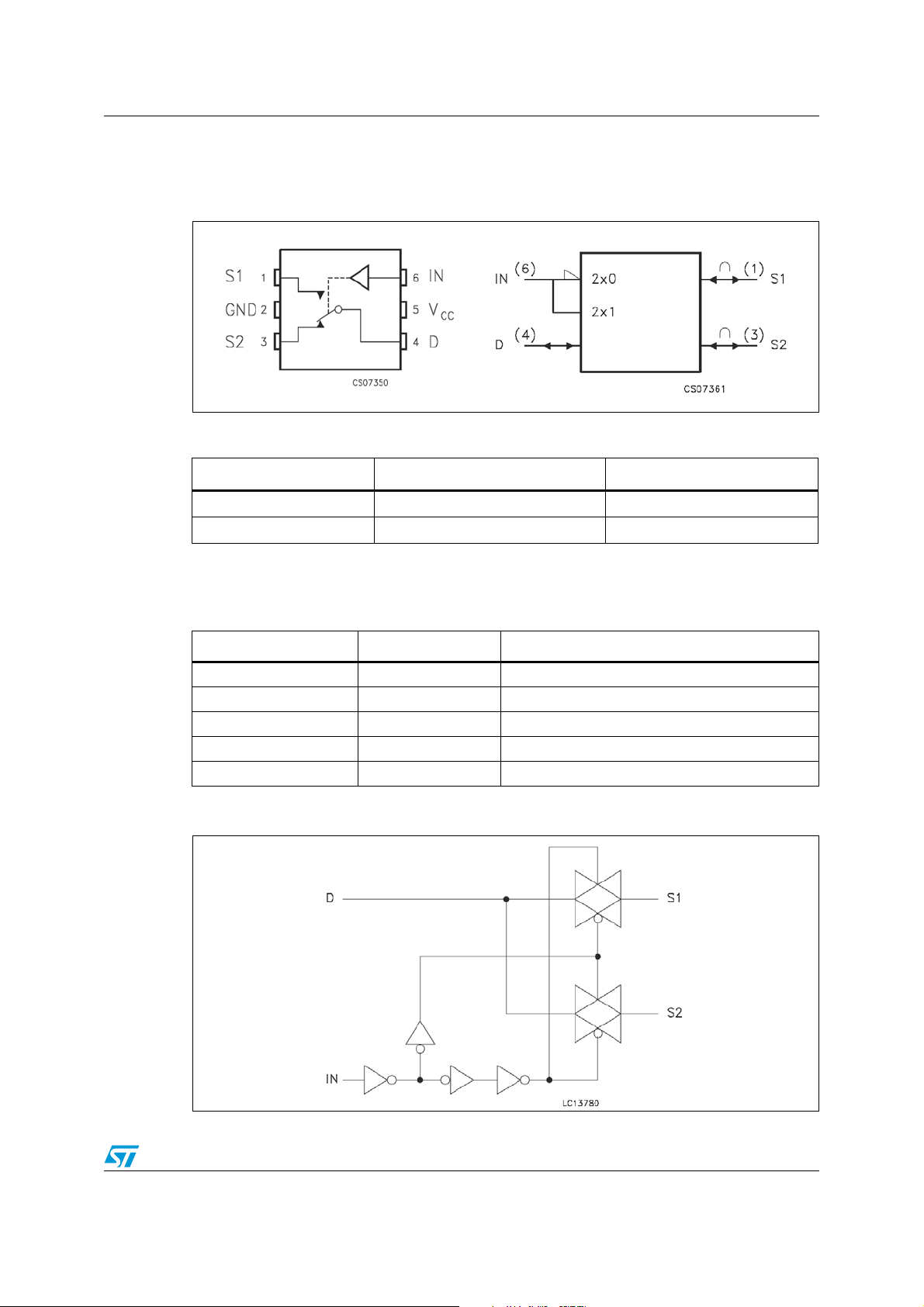
1 Pin connections and functions
Figure 1. Pin connections and IEC logic symbols
Table 2. Truth table
IN Switch S1 Switch S2
HONOFF
LOFF
(1)
(1)
ON
1. High impedance
Table 3. Pin descriptions
Pin Nº Symbol Name and function
1, 3 S1, S2 Independent channels
4 D Common channels
6INControl
5V
CC
2 GND Ground (0 V)
Figure 2. Input equivalent circuit
Positive supply voltage
Doc ID 9007 Rev 2 3/18

Electrical ratings STG3157
2 Electrical ratings
Stressing the device above the ratings listed in the “Absolute maximum ratings” table may
cause permanent damage to the device. These are stress ratings only and operation of the
device at these or any other conditions above those indicated in the operating sections of
this specification is not implied. Exposure to absolute maximum rating conditions for
extended periods may affect device reliability. Refer also to the STMicroelectronics SURE
Program and other relevant quality documents.
Table 4. Absolute maximum ratings
Symbol Parameter Value Unit
V
CC
V
V
IC
V
O
I
IKC
I
IK
I
OK
I
O
I
or I
CC
T
stg
T
L
Supply voltage -0.5 to +7.0 V
DC input voltage -0.5 to VCC + 0.5 V
I
DC control input voltage -0.5 to VCC + 0.5 V
DC output voltage -0.5 to VCC + 0.5 V
DC input diode current on control pin (V
DC input diode current (V
< 0V) ±50 mA
IN
< 0V) ±50 mA
IN
DC output diode current ±20 mA
DC output current +128 mA
DC VCC or ground current ±100 mA
GND
Storage temperature -65 to 150 °C
Lead temperature (10 s) 300 °C
Table 5. Recommended operating conditions
Symbol Parameter Value Unit
V
CC
V
V
IC
V
O
T
op
dt/dv
1. Truth table guaranteed: 1.2 V to 6.0 V
Supply voltage
Input voltage 0 to V
I
Control input voltage 0 to 5.5 V
Output voltage 0 to V
Operating temperature -55 to 125 °C
Input rise and fall time
control input
(1)
= 1.65V to 2.7V 0 to 20
V
CC
= 3.0 to 4.5V 0 to 10
V
CC
1.65 to 4.5 V
CC
CC
V
V
ns/V
4/18 Doc ID 9007 Rev 2
STG3157 Electrical characteristics
3 Electrical characteristics
3.1 DC Electrical characteristics
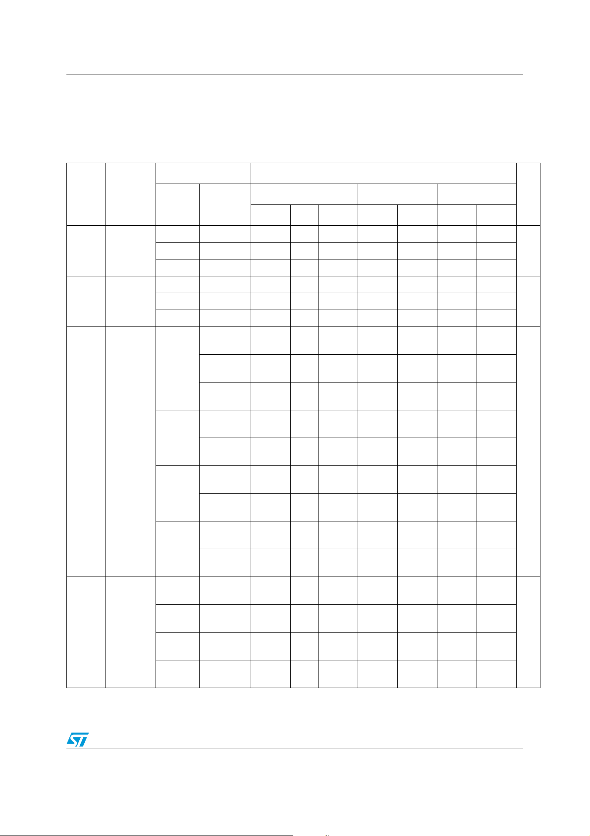
Table 6. DC specifications
Test conditions Value
Symbol Parameter
V
IH
V
IL
R
ON
ΔR
ON
High level
input
voltage
Low level
input
voltage
Switch onresistance
Onresistance
match
between
channels
TA = 25°C -40 to 85°C -55 to 125°C
Vcc (V)
Min. Typ. Max. Min. Max. Min. Max.
1.65-1.95 0.75V
CC
CC
0.75V
0.7V
CC
CC
0.75V
0.7V
CC
CC
2.7-3.6 2 2 2
1.65-1.95 0.25V
CC
CC
0.25V
0.3V
CC
CC
0.25V
0.3V
2.7-3.6 0.8 0.8 0.8
V
= 0V
4.5
3.0
S
= 30mA
I
S
= 2.4V
V
S
IS = 30mA
V
= 4.5V
S
IS = 30mA
= 0V
V
S
= 100mA
I
S
= 3V
V
S
IS = 24mA
V
= 0V
S
IS = 8mA
4.4 7 7 9
4.9 12 12 14.5
6.1 15 15 18
5.2 9 9 11
7.8 20 20 24
6.5 12 12 14.5
2.3
= 2.3V
V
1.65
4.5
3.0
2.3
1.65
S
= 8mA
I
S
= 0V
V
S
= 4mA
I
S
V
= 1.65V
S
IS = 4mA
= 3.15V
V
S
= 30mA
I
S
= 2.1V
V
S
IS = 24mA
V
= 1.6V
S
IS = 8mA
= 1.15V
V
S
= 4mA
I
S
9.6 30 30 36
9.0 20 20 24
14 50 50 60
0.10
0.10
0.20
0.35
CC
Unit
V2.3-2.5 0.7V
CC
V2.3-2.5 0.3V
Ω
Ω
Doc ID 9007 Rev 2 5/18
Electrical characteristics STG3157
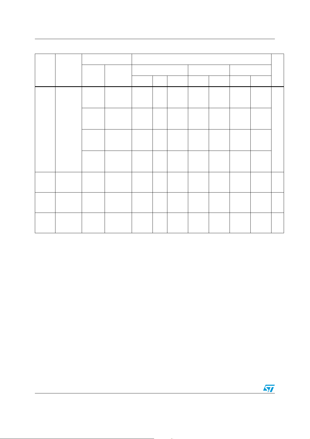
Table 6. DC specifications (continued)
Test conditions Value
Symbol Parameter
On-
R
FLAT
resistance
flatness
OFF state
OFF
leakage
I
current
Input
I
leakage
IN
current
Quiescent
I
supply
CC
current
Vcc (V)
5.0
3.3
2.5
1.8
1.65-195
0 - 5.5
1.65 - 4.3
= 0V to
V
S
V
CC
IS = 30mA
= 0V to
V
S
V
CC
IS = 24mA
= 0V to
V
S
V
CC
IS = 8mA
= 0V to
V
S
V
CC
IS = 4mA
V
= 0 to
S
V
CC
V
= 0 to
IN
5.5V
V
= VCC
IN
or GND
TA = 25°C -40 to 85°C -55 to 125°C
Min. Typ. Max. Min. Max. Min. Max.
3
6
14
80
±0.05
±0.05
±0.1 ±1 ±10 μA
±0.1 ±1 ±10 μA
1110μA
Unit
Ω
6/18 Doc ID 9007 Rev 2
 Loading...