

Page 1
Front panel controller/driver with standby
power management and real-time clock
Features
■ IC front panel VFD controller driver
■ Standby power management to the host
■ 3.3 V (V
supply for the IC
■ IR remote control decoder
(Philips, NEC, Thomson, Sony, Matsushita)
■ Multiple display modes
(12 seg. and 16 digits to 20 seg and 8 digits)
■ High voltage outputs (V
■ No additional external resistors required for
driver outputs (P-CH. open drain + pull-down
resistor outputs)
■ Key scanning (up to 12 x 2 matrix = 24 keys)
■ LED ports (4 channels 20 mA max each)
■ Serial I
communication protocol b
■ Operating speed: up to 400 kHz for I
■ Programmable hotkeys for IR remote con tr ol
command and KEYSCAN command
■ Low power consumption in standby mode
■ Dimming circuit (8 steps)
■ Real-time clock (accuracy ± 25 secs/month)
■ Wake-up alarm
■ Internal oscillator with external crystal for RTC
■ Available in PQFP-52 package (0.65 mm pitc h
Applications
) and down to -30 V (VSS)
DD
- 33.3 V max)
DD
2
C interface (SCL, SDA)
2
C
STFPC320
PQFP-52
Description
The STFPC320 is designed to integrate the VFD
driving, key-scan matrix, LED driving, infrared (I R)
remote control decoding and real-time clock
(RTC) into one integrated solution. All the
functions are programmable using the I
Low power consumpt ion is achieved during
standby operation. The STFPC320 provides the
standby power management to the main chipset.
The STFPC320 is housed in a 52-pin PQFP
package. The pin assignments and application
circuit are optimized for an easy PCB layout and
cost saving advantages.
2
C bus.
■ VCR, DVD and personal video recorders
■ Home theatre with clock feature, STB and HTiB
(home theater in a box)
Table 1. Device summary
Order code Operating temperature Package Packaging
STFPC320 -40°C to 85°C PQFP-52 Tape and reel
July 2008 Rev 2 1/78
www.st.com
78
Page 2

Contents STFPC320
Contents
1 Device block diagram . . . . . . . . . . . . . . . . . . . . . . . . . . . . . . . . . . . . . . . . 9
2 Functional diagram . . . . . . . . . . . . . . . . . . . . . . . . . . . . . . . . . . . . . . . . . 10
3 Pin settings . . . . . . . . . . . . . . . . . . . . . . . . . . . . . . . . . . . . . . . . . . . . . . . 11
3.1 Pin connection . . . . . . . . . . . . . . . . . . . . . . . . . . . . . . . . . . . . . . . . . . . . . 11
3.2 Pin description . . . . . . . . . . . . . . . . . . . . . . . . . . . . . . . . . . . . . . . . . . . . . 12
4 Functional description . . . . . . . . . . . . . . . . . . . . . . . . . . . . . . . . . . . . . . 13
4.1 Reset . . . . . . . . . . . . . . . . . . . . . . . . . . . . . . . . . . . . . . . . . . . . . . . . . . . . 13
4.2 Cold boot up . . . . . . . . . . . . . . . . . . . . . . . . . . . . . . . . . . . . . . . . . . . . . . . 14
4.3 Entering standby mode . . . . . . . . . . . . . . . . . . . . . . . . . . . . . . . . . . . . . . 15
4.4 Wake-up . . . . . . . . . . . . . . . . . . . . . . . . . . . . . . . . . . . . . . . . . . . . . . . . . . 16
4.5 Interrupts/events handling by STFPC320 . . . . . . . . . . . . . . . . . . . . . . . . . 17
4.6 Ready pin . . . . . . . . . . . . . . . . . . . . . . . . . . . . . . . . . . . . . . . . . . . . . . . . . 17
4.7 Mute pin . . . . . . . . . . . . . . . . . . . . . . . . . . . . . . . . . . . . . . . . . . . . . . . . . . 18
4.8 Keyscan matrix/front panel keys . . . . . . . . . . . . . . . . . . . . . . . . . . . . . . . . 18
4.9 LED ports . . . . . . . . . . . . . . . . . . . . . . . . . . . . . . . . . . . . . . . . . . . . . . . . . 18
4.10 Display . . . . . . . . . . . . . . . . . . . . . . . . . . . . . . . . . . . . . . . . . . . . . . . . . . . 18
4.10.1 Normal display . . . . . . . . . . . . . . . . . . . . . . . . . . . . . . . . . . . . . . . . . . . . 18
4.10.2 RTC display . . . . . . . . . . . . . . . . . . . . . . . . . . . . . . . . . . . . . . . . . . . . . . 18
4.11 Remote control decoder . . . . . . . . . . . . . . . . . . . . . . . . . . . . . . . . . . . . . . 19
4.12 PIN_AV8 . . . . . . . . . . . . . . . . . . . . . . . . . . . . . . . . . . . . . . . . . . . . . . . . . . 19
4.13 Default state upon power-up . . . . . . . . . . . . . . . . . . . . . . . . . . . . . . . . . . 19
4.14 Initial state . . . . . . . . . . . . . . . . . . . . . . . . . . . . . . . . . . . . . . . . . . . . . . . . 20
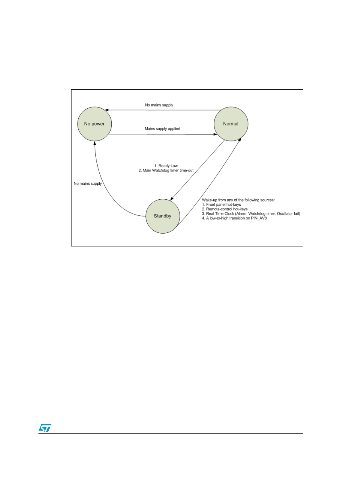
5 Operating state diagram . . . . . . . . . . . . . . . . . . . . . . . . . . . . . . . . . . . . . 21
6 Real-time clock (RTC) operation . . . . . . . . . . . . . . . . . . . . . . . . . . . . . . 22
6.1 Real-time clock . . . . . . . . . . . . . . . . . . . . . . . . . . . . . . . . . . . . . . . . . . . . . 22
6.2 2-wire bus characteristics . . . . . . . . . . . . . . . . . . . . . . . . . . . . . . . . . . . . . 22
6.3 Watchdog timer . . . . . . . . . . . . . . . . . . . . . . . . . . . . . . . . . . . . . . . . . . . . 24
2/78
Page 3

STFPC320 Contents
6.4 Real-time clock (RTC) . . . . . . . . . . . . . . . . . . . . . . . . . . . . . . . . . . . . . . . 24
6.4.1 Reading the real-time clock . . . . . . . . . . . . . . . . . . . . . . . . . . . . . . . . . . 25
6.4.2 Writing to the real-time clock . . . . . . . . . . . . . . . . . . . . . . . . . . . . . . . . . 25
6.5 Register table for RTC . . . . . . . . . . . . . . . . . . . . . . . . . . . . . . . . . . . . . . . 26
6.6 Setting alarm clock registers . . . . . . . . . . . . . . . . . . . . . . . . . . . . . . . . . . 27
6.7 Calibrating the clock . . . . . . . . . . . . . . . . . . . . . . . . . . . . . . . . . . . . . . . . . 28
6.8 Square wave output . . . . . . . . . . . . . . . . . . . . . . . . . . . . . . . . . . . . . . . . . 30
6.9 Century bits . . . . . . . . . . . . . . . . . . . . . . . . . . . . . . . . . . . . . . . . . . . . . . . 31
6.10 Oscillator stop detection . . . . . . . . . . . . . . . . . . . . . . . . . . . . . . . . . . . . . . 31
6.11 Initial power-on defaults . . . . . . . . . . . . . . . . . . . . . . . . . . . . . . . . . . . . . . 32
7 Commands . . . . . . . . . . . . . . . . . . . . . . . . . . . . . . . . . . . . . . . . . . . . . . . . 33
7.1 Configuration mode setting command . . . . . . . . . . . . . . . . . . . . . . . . . . . 33
7.2 Data setting command . . . . . . . . . . . . . . . . . . . . . . . . . . . . . . . . . . . . . . . 36
7.3 Display control and hotkey setting command . . . . . . . . . . . . . . . . . . . . . . 38
7.4 Example for device configuration . . . . . . . . . . . . . . . . . . . . . . . . . . . . . . . 41
8 Key matrix . . . . . . . . . . . . . . . . . . . . . . . . . . . . . . . . . . . . . . . . . . . . . . . . 42
8.1 Key read sequence . . . . . . . . . . . . . . . . . . . . . . . . . . . . . . . . . . . . . . . . . . 43
9 LED port . . . . . . . . . . . . . . . . . . . . . . . . . . . . . . . . . . . . . . . . . . . . . . . . . . 44
9.1 Writing to LED sequence . . . . . . . . . . . . . . . . . . . . . . . . . . . . . . . . . . . . . 44
10 SW data . . . . . . . . . . . . . . . . . . . . . . . . . . . . . . . . . . . . . . . . . . . . . . . . . . 45
10.1 Reading switch sequence . . . . . . . . . . . . . . . . . . . . . . . . . . . . . . . . . . . . 45
11 Address setting command . . . . . . . . . . . . . . . . . . . . . . . . . . . . . . . . . . . 46
11.1 RTC display data read . . . . . . . . . . . . . . . . . . . . . . . . . . . . . . . . . . . . . . . 46
11.2 Display (normal & RTC) data write . . . . . . . . . . . . . . . . . . . . . . . . . . . . . . 46
12 Normal display memory locations . . . . . . . . . . . . . . . . . . . . . . . . . . . . . 47
13 Configuration data . . . . . . . . . . . . . . . . . . . . . . . . . . . . . . . . . . . . . . . . . 48
14 Interrupt flags . . . . . . . . . . . . . . . . . . . . . . . . . . . . . . . . . . . . . . . . . . . . . 50
3/78
Page 4

Contents STFPC320
15 Remote control protocols . . . . . . . . . . . . . . . . . . . . . . . . . . . . . . . . . . . . 51
15.1 Decoded and RAW formats . . . . . . . . . . . . . . . . . . . . . . . . . . . . . . . . . . . 51
15.2 Sending IR data on I
15.3 Philips RC-5 remote control protocol . . . . . . . . . . . . . . . . . . . . . . . . . . . . 52
15.3.1 RC-5 data in decoded format . . . . . . . . . . . . . . . . . . . . . . . . . . . . . . . . . 53
15.3.2 RC-5 data in RAW format . . . . . . . . . . . . . . . . . . . . . . . . . . . . . . . . . . . 53
15.4 NEC remote control protocol . . . . . . . . . . . . . . . . . . . . . . . . . . . . . . . . . . 54
15.4.1 NEC in decoded format . . . . . . . . . . . . . . . . . . . . . . . . . . . . . . . . . . . . . 55
15.4.2 NEC in RAW format . . . . . . . . . . . . . . . . . . . . . . . . . . . . . . . . . . . . . . . . 55
15.5 Sony remote control format . . . . . . . . . . . . . . . . . . . . . . . . . . . . . . . . . . . 56
15.5.1 Sony in decoded format . . . . . . . . . . . . . . . . . . . . . . . . . . . . . . . . . . . . . 57
15.5.2 Sony in RAW format . . . . . . . . . . . . . . . . . . . . . . . . . . . . . . . . . . . . . . . 57
15.6 Matsushita remote control format . . . . . . . . . . . . . . . . . . . . . . . . . . . . . . . 58
15.6.1 Matsushita in decoded format . . . . . . . . . . . . . . . . . . . . . . . . . . . . . . . . 59
15.6.2 Matsushita in RAW format . . . . . . . . . . . . . . . . . . . . . . . . . . . . . . . . . . . 60
2
C interface . . . . . . . . . . . . . . . . . . . . . . . . . . . . . . . 51
15.7 R2000 remote control format . . . . . . . . . . . . . . . . . . . . . . . . . . . . . . . . . . 61
15.7.1 R2000 in decoded format . . . . . . . . . . . . . . . . . . . . . . . . . . . . . . . . . . . 62
15.7.2 R2000 in RAW format . . . . . . . . . . . . . . . . . . . . . . . . . . . . . . . . . . . . . . 62
15.8 RCA remote control format . . . . . . . . . . . . . . . . . . . . . . . . . . . . . . . . . . . . 63
15.8.1 RCA in decoded format . . . . . . . . . . . . . . . . . . . . . . . . . . . . . . . . . . . . . 64
15.8.2 RCA in RAW format . . . . . . . . . . . . . . . . . . . . . . . . . . . . . . . . . . . . . . . . 64
16 Serial communication format . . . . . . . . . . . . . . . . . . . . . . . . . . . . . . . . . 65
17 Electrical characteristics . . . . . . . . . . . . . . . . . . . . . . . . . . . . . . . . . . . . 68
17.1 Absolute maximum ratings . . . . . . . . . . . . . . . . . . . . . . . . . . . . . . . . . . . . 68
17.2 Recommended operating conditions . . . . . . . . . . . . . . . . . . . . . . . . . . . . 68
17.3 Power consumption estimation . . . . . . . . . . . . . . . . . . . . . . . . . . . . . . . . . 69
17.4 Electrical specifications . . . . . . . . . . . . . . . . . . . . . . . . . . . . . . . . . . . . . . 70
17.5 Crystal electrical characteristics . . . . . . . . . . . . . . . . . . . . . . . . . . . . . . . . 71
17.6 Oscillator characteristics . . . . . . . . . . . . . . . . . . . . . . . . . . . . . . . . . . . . . 71
17.7 Timing characteristics . . . . . . . . . . . . . . . . . . . . . . . . . . . . . . . . . . . . . . . 72
17.8 Switching characteristics . . . . . . . . . . . . . . . . . . . . . . . . . . . . . . . . . . . . . 73
18 STFPC320 typical application circuit . . . . . . . . . . . . . . . . . . . . . . . . . . 74
4/78
Page 5

STFPC320 Contents
19 Package mechanical data . . . . . . . . . . . . . . . . . . . . . . . . . . . . . . . . . . . . 75
20 Revision history . . . . . . . . . . . . . . . . . . . . . . . . . . . . . . . . . . . . . . . . . . . 77
5/78
Page 6

List of tables STFPC320
List of tables
Table 1. Device summary. . . . . . . . . . . . . . . . . . . . . . . . . . . . . . . . . . . . . . . . . . . . . . . . . . . . . . . . . . 1
Table 2. Pin description . . . . . . . . . . . . . . . . . . . . . . . . . . . . . . . . . . . . . . . . . . . . . . . . . . . . . . . . . . 12
Table 3. Default state . . . . . . . . . . . . . . . . . . . . . . . . . . . . . . . . . . . . . . . . . . . . . . . . . . . . . . . . . . . . 19
Table 4. Register table for RTC . . . . . . . . . . . . . . . . . . . . . . . . . . . . . . . . . . . . . . . . . . . . . . . . . . . . 26
Table 5. Alarm repeat modes . . . . . . . . . . . . . . . . . . . . . . . . . . . . . . . . . . . . . . . . . . . . . . . . . . . . . . 27
Table 6. Square wave output frequency . . . . . . . . . . . . . . . . . . . . . . . . . . . . . . . . . . . . . . . . . . . . . . 30
Table 7. Century bits. . . . . . . . . . . . . . . . . . . . . . . . . . . . . . . . . . . . . . . . . . . . . . . . . . . . . . . . . . . . . 31
Table 8. Initial power-on default values of the registers . . . . . . . . . . . . . . . . . . . . . . . . . . . . . . . . . . 32
Table 9. Data write command. b5 b4: 00 . . . . . . . . . . . . . . . . . . . . . . . . . . . . . . . . . . . . . . . . . . . . . 36
Table 10. Data read 1 command. b5 b4: 10 . . . . . . . . . . . . . . . . . . . . . . . . . . . . . . . . . . . . . . . . . . . . 36
Table 11. Data read 2 command. b5 b4: 11 . . . . . . . . . . . . . . . . . . . . . . . . . . . . . . . . . . . . . . . . . . . . 36
Table 12. Display RAM address and display mode . . . . . . . . . . . . . . . . . . . . . . . . . . . . . . . . . . . . . . 47
Table 13. Sony remote control format . . . . . . . . . . . . . . . . . . . . . . . . . . . . . . . . . . . . . . . . . . . . . . . . 56
Table 14. Matsushita remote control format . . . . . . . . . . . . . . . . . . . . . . . . . . . . . . . . . . . . . . . . . . . . 59
Table 15. Absolute maximum ratings (TA = 25°C, GND = 0 V) . . . . . . . . . . . . . . . . . . . . . . . . . . . . . 68
Table 16. Recommended operating conditions (T
Table 17. Electrical specifications
(T
= -20 to +70 °C, VDD = 3.3 V, GND = 0 V, VSS = VDD – 33.3 V)70
A
Table 18. Crystal electrical characteristics . . . . . . . . . . . . . . . . . . . . . . . . . . . . . . . . . . . . . . . . . . . . . 71
Table 19. Oscillator characteristics. . . . . . . . . . . . . . . . . . . . . . . . . . . . . . . . . . . . . . . . . . . . . . . . . . . 71
Table 20. Switching characterist ics
(T
= -20 to +70 °C, VDD = 3.3V, VSS = -30V)73
Table 21. Switching characterist ics (T
A
= -20 to +70 °C, VDD = 3.3V, VSS = -30V) . . . . . . . . . . . . . . 73
A
Table 22. PQFP52 (10 x 10 x 2 mm) mechanical data. . . . . . . . . . . . . . . . . . . . . . . . . . . . . . . . . . . . 76
Table 23. Document revision history . . . . . . . . . . . . . . . . . . . . . . . . . . . . . . . . . . . . . . . . . . . . . . . . . 77
= -20 to +70°C, GND = 0V) . . . . . . . . . . . . . . . . 68
A
6/78
Page 7

STFPC320 List of figures
List of figures
Figure 1. STFPC320 block diagram. . . . . . . . . . . . . . . . . . . . . . . . . . . . . . . . . . . . . . . . . . . . . . . . . . . 8
Figure 2. Functional diagram . . . . . . . . . . . . . . . . . . . . . . . . . . . . . . . . . . . . . . . . . . . . . . . . . . . . . . . . 9
Figure 3. Pin connection (top view) . . . . . . . . . . . . . . . . . . . . . . . . . . . . . . . . . . . . . . . . . . . . . . . . . . 10
Figure 4. Power-up behaviour . . . . . . . . . . . . . . . . . . . . . . . . . . . . . . . . . . . . . . . . . . . . . . . . . . . . . . 13
Figure 5. Standby mode behaviour . . . . . . . . . . . . . . . . . . . . . . . . . . . . . . . . . . . . . . . . . . . . . . . . . . 14
Figure 6. Wake-up . . . . . . . . . . . . . . . . . . . . . . . . . . . . . . . . . . . . . . . . . . . . . . . . . . . . . . . . . . . . . . . 15
Figure 7. Interrupts/events handling . . . . . . . . . . . . . . . . . . . . . . . . . . . . . . . . . . . . . . . . . . . . . . . . . 16
Figure 8. Operating state diagram . . . . . . . . . . . . . . . . . . . . . . . . . . . . . . . . . . . . . . . . . . . . . . . . . . . 20
Figure 9. Serial bus data transfer sequence . . . . . . . . . . . . . . . . . . . . . . . . . . . . . . . . . . . . . . . . . . . 2 2
Figure 10. Acknowledgement sequence . . . . . . . . . . . . . . . . . . . . . . . . . . . . . . . . . . . . . . . . . . . . . . . 22
Figure 11. Alarm interrupt reset waveform. . . . . . . . . . . . . . . . . . . . . . . . . . . . . . . . . . . . . . . . . . . . . . 26
Figure 12. Crystal accuracy across temperature . . . . . . . . . . . . . . . . . . . . . . . . . . . . . . . . . . . . . . . . . 28
Figure 13. Calibrating waveform . . . . . . . . . . . . . . . . . . . . . . . . . . . . . . . . . . . . . . . . . . . . . . . . . . . . . 28
Figure 14. First byte format after configuration byte . . . . . . . . . . . . . . . . . . . . . . . . . . . . . . . . . . . . . . 33
Figure 15. Second byte format after configuration byte. . . . . . . . . . . . . . . . . . . . . . . . . . . . . . . . . . . . 34
Figure 16. 14-segment + dotpoint display . . . . . . . . . . . . . . . . . . . . . . . . . . . . . . . . . . . . . . . . . . . . . . 38
Figure 17. Front panel hotkeys configuration. . . . . . . . . . . . . . . . . . . . . . . . . . . . . . . . . . . . . . . . . . . . 39
Figure 18. Key matrix and key-input data storage RAM . . . . . . . . . . . . . . . . . . . . . . . . . . . . . . . . . . . 41
Figure 19. LED byte format . . . . . . . . . . . . . . . . . . . . . . . . . . . . . . . . . . . . . . . . . . . . . . . . . . . . . . . . . 43
Figure 20. LED byte format . . . . . . . . . . . . . . . . . . . . . . . . . . . . . . . . . . . . . . . . . . . . . . . . . . . . . . . . . 44
Figure 21. Configuration data bytes. . . . . . . . . . . . . . . . . . . . . . . . . . . . . . . . . . . . . . . . . . . . . . . . . . . 47
Figure 22. Configuration data bytes (continued) . . . . . . . . . . . . . . . . . . . . . . . . . . . . . . . . . . . . . . . . . 48
Figure 23. Interrupt byte format . . . . . . . . . . . . . . . . . . . . . . . . . . . . . . . . . . . . . . . . . . . . . . . . . . . . . . 49
Figure 24. IR data format. . . . . . . . . . . . . . . . . . . . . . . . . . . . . . . . . . . . . . . . . . . . . . . . . . . . . . . . . . . 50
Figure 25. Bi-phase coding . . . . . . . . . . . . . . . . . . . . . . . . . . . . . . . . . . . . . . . . . . . . . . . . . . . . . . . . . 51
Figure 26. RC-5 protocol frame . . . . . . . . . . . . . . . . . . . . . . . . . . . . . . . . . . . . . . . . . . . . . . . . . . . . . . 51
Figure 27. Example of RC-5 transmission . . . . . . . . . . . . . . . . . . . . . . . . . . . . . . . . . . . . . . . . . . . . . . 51
Figure 28. RC-5 data structure in decoded format. . . . . . . . . . . . . . . . . . . . . . . . . . . . . . . . . . . . . . . . 52
Figure 29. RC-5 data structure in raw format. . . . . . . . . . . . . . . . . . . . . . . . . . . . . . . . . . . . . . . . . . . . 52
Figure 30. Pulse distance modulation . . . . . . . . . . . . . . . . . . . . . . . . . . . . . . . . . . . . . . . . . . . . . . . . . 53
Figure 31. The transmitted waveform for NEC protocol. . . . . . . . . . . . . . . . . . . . . . . . . . . . . . . . . . . . 53
Figure 32. NEC data structure in decoded format . . . . . . . . . . . . . . . . . . . . . . . . . . . . . . . . . . . . . . . . 54
Figure 33. NEC data structure in raw format . . . . . . . . . . . . . . . . . . . . . . . . . . . . . . . . . . . . . . . . . . . . 54
Figure 34. Output code waveform timing definitions . . . . . . . . . . . . . . . . . . . . . . . . . . . . . . . . . . . . . . 55
Figure 35. Sony data structure in decoded format. . . . . . . . . . . . . . . . . . . . . . . . . . . . . . . . . . . . . . . . 56
Figure 36. Sony data structure in raw format. . . . . . . . . . . . . . . . . . . . . . . . . . . . . . . . . . . . . . . . . . . . 56
Figure 37. Matsushita remote control protocol. . . . . . . . . . . . . . . . . . . . . . . . . . . . . . . . . . . . . . . . . . . 57
Figure 38. Matsushita data structure in decoded format . . . . . . . . . . . . . . . . . . . . . . . . . . . . . . . . . . . 58
Figure 39. Matsushita data structure in raw format . . . . . . . . . . . . . . . . . . . . . . . . . . . . . . . . . . . . . . . 59
Figure 40. Thomson R2000 remote control protocol . . . . . . . . . . . . . . . . . . . . . . . . . . . . . . . . . . . . . . 60
Figure 41. R2000 data structure in decoded format . . . . . . . . . . . . . . . . . . . . . . . . . . . . . . . . . . . . . . 61
Figure 42. R2000 data structure in raw format . . . . . . . . . . . . . . . . . . . . . . . . . . . . . . . . . . . . . . . . . . 61
Figure 43. Thomson RCA remote control protocol . . . . . . . . . . . . . . . . . . . . . . . . . . . . . . . . . . . . . . . 62
Figure 44. RCA data structure in decoded format . . . . . . . . . . . . . . . . . . . . . . . . . . . . . . . . . . . . . . . . 63
Figure 45. RCA data structure in raw format . . . . . . . . . . . . . . . . . . . . . . . . . . . . . . . . . . . . . . . . . . . . 63
Figure 46. Complete data transfer . . . . . . . . . . . . . . . . . . . . . . . . . . . . . . . . . . . . . . . . . . . . . . . . . . . . 64
Figure 47. Valid data changes on the SDA bus. . . . . . . . . . . . . . . . . . . . . . . . . . . . . . . . . . . . . . . . . . 64
Figure 48. Valid start and stop conditions . . . . . . . . . . . . . . . . . . . . . . . . . . . . . . . . . . . . . . . . . . . . . . 64
7/78
Page 8

List of figures STFPC320
Figure 49. Acknowledge response from receiver. . . . . . . . . . . . . . . . . . . . . . . . . . . . . . . . . . . . . . . . . 64
Figure 50. Bus timing requirements sequence . . . . . . . . . . . . . . . . . . . . . . . . . . . . . . . . . . . . . . . . . . 65
Figure 51. Slave address location . . . . . . . . . . . . . . . . . . . . . . . . . . . . . . . . . . . . . . . . . . . . . . . . . . . . 65
Figure 52. Read mode sequence. . . . . . . . . . . . . . . . . . . . . . . . . . . . . . . . . . . . . . . . . . . . . . . . . . . . . 65
Figure 53. Alternative READ mode sequence . . . . . . . . . . . . . . . . . . . . . . . . . . . . . . . . . . . . . . . . . . . 66
Figure 54. WRITE mode sequence . . . . . . . . . . . . . . . . . . . . . . . . . . . . . . . . . . . . . . . . . . . . . . . . . . . 66
Figure 55. Key scanning and display timing . . . . . . . . . . . . . . . . . . . . . . . . . . . . . . . . . . . . . . . . . . . . 71
Figure 56. Typical application circuit . . . . . . . . . . . . . . . . . . . . . . . . . . . . . . . . . . . . . . . . . . . . . . . . . . 73
Figure 57. PQFP52L package outline . . . . . . . . . . . . . . . . . . . . . . . . . . . . . . . . . . . . . . . . . . . . . . . . . 74
8/78
Page 9
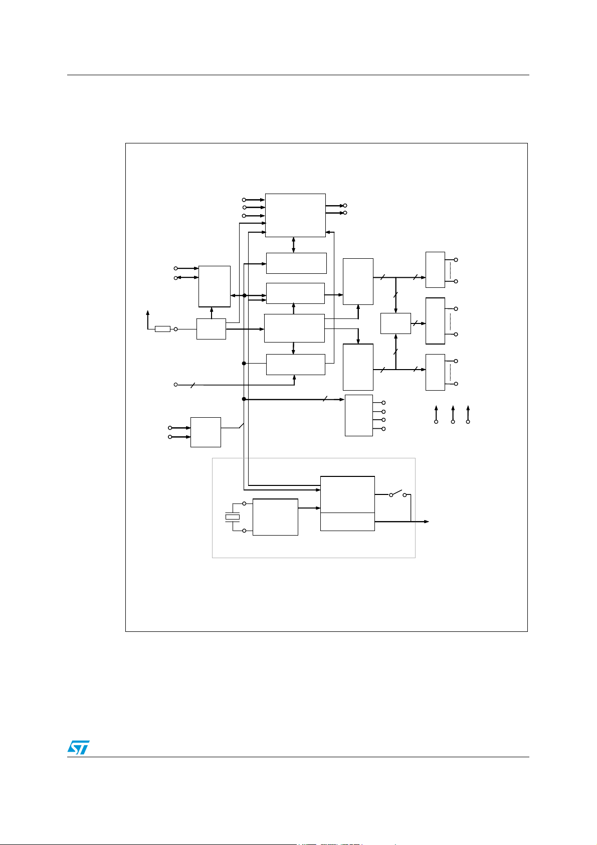
STFPC320 Device block diagram
1 Device block diagram
Figure 1. STFPC320 block diagram
IR_DATA_IN
VDD
VDD
SW1
SW1
SW2
SW2
SCL
SCL
SDA
SDA
R
R
Key1
Key1
Key2
Key2
IR_DATA_IN
Serial
Serial
OSC
OSC
2
2
2-bit
2-bit
Latc h
Latc h
READY
READY
PIN_AV8
PIN_AV8
I2C
I2C
I/F
I/F
Remote Control
Remote Control
Decoder & Stand
Decoder & Stand
By Function
By Function
Command Decoder
Command Decoder
Display Memory
Display Memory
(20 x 16)
(20 x 16)
Timing Generator
Timing Generator
Key Scan and
Key Scan and
Dimming Circuit
Dimming Circuit
Key Data Mem ory
Key Data Mem ory
(2 x 12)
(2 x 12)
32 KHz
32 KHz
oscillator
oscillator
MUTE
MUTE
STBY
STBY
20-bit
20-bit
Output
Output
Latc h
Latc h
16-bit
16-bit
Shift
Shift
Register
Register
4
4
4-bit
4-bit
Latch
Latch
Real-time Clock
Real-time Clock
Real-time Clock
Real-time Clock
Calendar
Calendar
RTC wit h Alarm
RTC wit h Alarm
& Calibrat ion
& Calibrat ion
Watchdog
Watchdog
20 12
20 12
8
8
Data
Data
Selector
Selector
8
8
16
16
LED1
LED1
LED2
LED2
LED3
LED3
LED4
LED4
AFE
AFE
8
8
8
8
Drivers
Drivers
Segment
Segment
Drivers
Drivers
Multiplexed
Multiplexed
Grid
Grid
Drivers
Drivers
VDD
VDD
(+3.3V)
(+3.3V)
IRQ_N/SQW
IRQ_N/SQW
SEG1/KS1
SEG1/KS1
SEG12/KS12
SEG12/KS12
SEG13/GRID16
SEG13/GRID16
SEG20/GRID9
SEG20/GRID9
GRID8
GRID8
GRID1
GRID1
GND
GND
(0V)
(0V)
(-30V)
(-30V)
VSS
VSS
9/78
Page 10
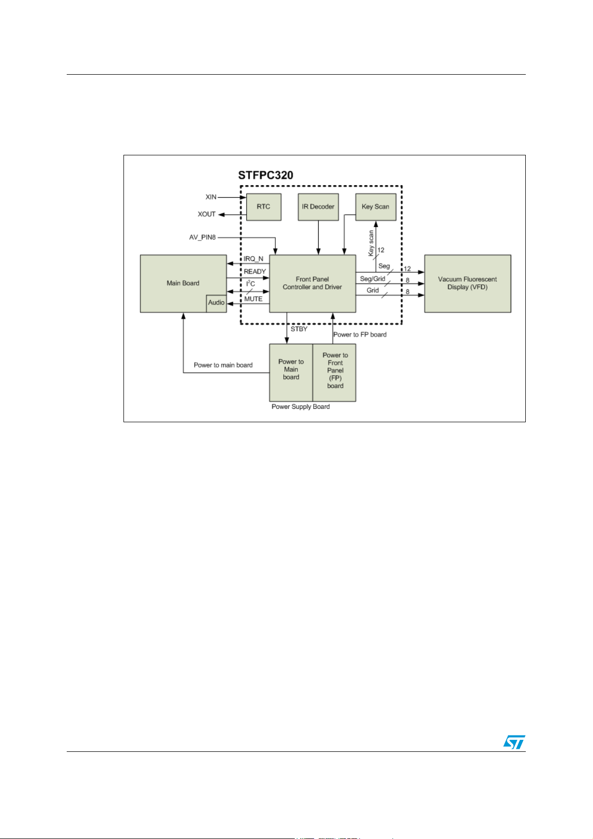
Functional diagram STFPC320
2 Functional diagram
Figure 2. Functional diagram
10/78
Page 11
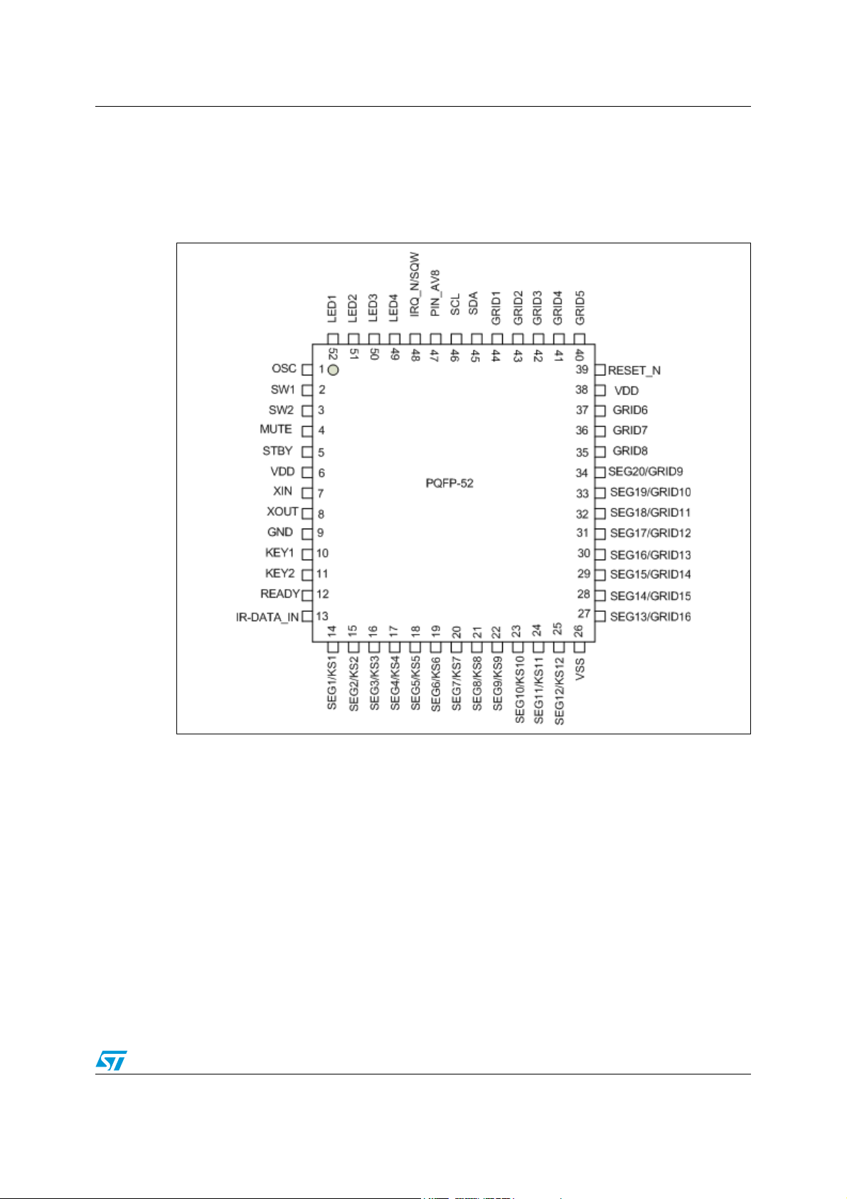
STFPC320 Pin settings
3 Pin settings
3.1 Pin connection
Figure 3. Pin connection (top view)
Note: For a description of each pin behaviour, please refer to the STFPC320 Table 2: Pin
description on page 12
11/78
Page 12

Pin settings STFPC320
3.2 Pin description
Table 2. Pin description
Pin N° Name Type Description
1 OSC IN Connect to an external resistor of value 33 kΩ ± 1%
2 SW1 IN General purpose switch input port.
3 SW2 IN General purpose switch input port.
4 MUTE OUT
5STBYOUT
6, 38 VDD SUPPLY 3.3 V ± 10%. Core main supply voltage.
7 XIN IN Oscillator input pin. 32.768 KHz crystal.
8 XOUT OUT Oscillator output pin. 32.768 KHz crystal.
9 GND SUPPLY Connect this pin to system GND.
10,11 KEY1, KEY2 IN
12 READY IN
13 IR_DATA_IN IN Remote control input. Connect to IR photodiode.
14 to 25
26 VSS SUPPLY VFD outputs high voltage pull-down level. VDD- 33.3 V max.
27 to 34
35-37 GRID8 to GRID6 OUT Grid output pins.
39 RESET_N IN Active low reset input.
SEG1/KS1 to
SEG12/KS12
SEG13/GRID16
to SEG20/GRID9
OUT Segment output pins (dual function as key source).
OUT These pins are selectable for segment or grid driving.
High level means mute status for audio.
Low level stands for normal working.
Pin to control power to the main board. High level means standby status.
Low level stands for normal working. Active high.
Input data to these pins from external keyboard are latched at end of the
display cycle (maximum keyboard size is 12 x 2).
High level on this pin means that main board chip has been working
normally. Connect an external pull down resistor of 10kΩ on this pin.
40-44 GRID5 to GRID1 OUT Grid output pins.
45 SDA IN/OUT Serial data in/out. Connect to 3.3 V through an external pull-up resistor.
46 SCL IN Serial clock input. Connect to 3.3 V through an external pull-up resistor.
A rising edge transition on this input will signal wake-up operation. This
47 PIN_AV8 IN
48 IRQ_N/SQW OUT
49, 50,
51, 52
12/78
LED4, LED3,
LED2, LED1
OUT CMOS sink outputs (20 mA max).
signal comes from the SCART interface. The micro processor can use this
signal to start the recording or take other actions.
Interrupt/square wave output (open drain). A pull up resistor of 10 kΩ must
be connected on this pin.
Page 13

STFPC320 Functional description
4 Functional description
The STFPC320 integrates the supply standby management functionality, remote control
decoder, a 2 8-bit VFD driver and a real-time cloc k (R TC). This d e vice is meant to reduce the
standby power consumption of the whole front panel application and also to reduce
hardware/cost by integrating the above mentioned functions in a single chip.
By utilizing the standby function, the host processor and other ICs could be turned off, thus
reducing the system power consumption. The STFPC 32 0 is able to wake-up the system
when programmed hotkeys are detected to signal that the full operation of the system is
required. The hotkeys could be entered to the system through the front panel keys or
through the infrared (IR) remote control. STFPC320 supports multiple remote control
protocols decoding by setting the appropriate register.
The integrated 28-bit VFD driver can drive up to 16 digits of display. Controlling of the
display is done through writing to a internal RAM. The 4 LED drivers allow indication of
operation of the system. 2-wire serial interface (I
host processor and STFPC320.
The STFPC320 integrates a a low-power serial RTC with a built-in 32.768kHz oscillator
(external crystal controlled). Eight bytes of the SRAM are used for the clock/calendar
function and are configured in bin ary coded decimal (BCD) f ormat. An additio nal 12 b ytes of
SRAM provide status/ control of alarm, watchdog and square wave functions. Addresses
and data are transf erred serially via a two line, bidirectional I
address register is incremented automatically after each WRITE or READ data byte.
2
C) completes the interfacing part between
2
C interface. The built-in
Functions available to the user include a non-volatile, time-of-day clock/calendar, alarm
interrupts, watchdog timer a nd progr ammab le Square W a v e output. T he eight cloc k address
locations contain the century, year, month, date, day, hour, minute, second and
tenths/hundredths of a second in 24 hour BCD format. Corrections for 28, 29 (leap year valid until year 2100), 30 and 31 day months are made automatically.
4.1 Reset
Reset is an active low input signal to the STFPC320. A negative pulse input on RESET_N
pin resets the STFPC320. Electrical specifications of this pin are identical to that of the logic
input pin.
Upon power-up, an internal power on reset circuit resets the whole chip. This occurs when
V
is ramping up (at appro xim ately 2.7 V) and the whole chip is initialized within 4 µs. This
DD
time is much lesser than the typical V
RESET_N pin permanently by a pull-up resistor to V
during normal operation. For an initia lization on po wer-up, a power-on-reset in STFPC320 is
sufficient to reset the entire STFPC320.
As soon as the 3.3 V supply to the chip is stable, the I
communication.
ramp-up time. It is recommended to tie the
DD
if reset to STFPC320 is not desired
DD
2
C bus of the STFPC320 is ready for
13/78
Page 14
Functional description STFPC320
4.2 Cold boot up
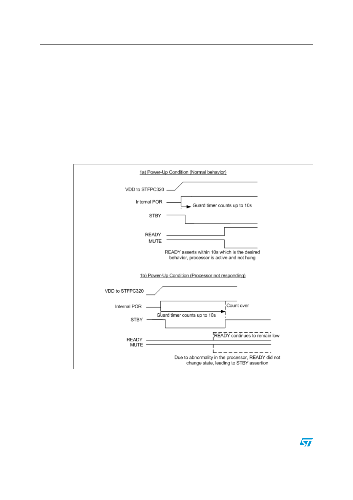
When power is first applied to the system, the STFPC320 will be reset. It will then manage
the power to the main board by bringing the STBY pin to a low level. This will wake-up the
main processor which will assert the READY pin to a high lev el to indicate to STFPC320 of a
proper boot-up sequence.
If the microprocessor does not assert the READY pin to a high within 10s, the STFPC320
will cut off the power to the Host by asserting the STBY pin. The high level on READY pin
signifies that the processor is ready. After this, the processor can configure the STFPC320
by sending the v arious I
mapping, hot-keys.
The power-up behavior in 2 conditions is shown in the Figure 4.
Figure 4. Power-up behaviour
2
C commands for configuration o f displa y, RC protocol, R TC displa y
Note: 1 Guard timer is turned off by default upon READY assertion.
2 If the guard timer is to be kept on during READY high condition, the guard timer registers
must be set accordingly by proper commands through I
2
C bus.
3 In this power-up condition, the guard timer is triggered by internal POR pulse.
4 During power-up, the guard timer value is 10s.
14/78
Page 15
STFPC320 Functional description
4.3 Entering standby mode
The STFPC320 will control the power to the main board using the STBY pin. During normal
operation, the STBY pin is at a low level which externally controls a power MOS switch to
enable power to the main board. The STFPC320 asserts the STBY pin to a high when any
one of the following condit ions occur:
● Processor fails to respond by enabling the READY pin within 10 s upon first power-up
(cold boot up)
● Guard timer counts down to 0 s
● Processor makes the READY pin to low (can happen in various conditions, such as
user presses STBY key on front panel, STBY key on remote control, etc.)
Figure 5. Standby mode behaviour
Note: 1 Guard timer can be kept on during normal condition when READY is high (depending on the
user).
2 In this condition, the guard timer can be disabled or enabled. If the guard timer is enabled,
the timer needs to be cleared before the programmed count o f the timer is reached. If the
programmed count is reached, the STBY will be asserted.
3 It is advisable not to enable the guard timer during normal operation.
15/78
Page 16
Functional description STFPC320
4.4 Wake-up
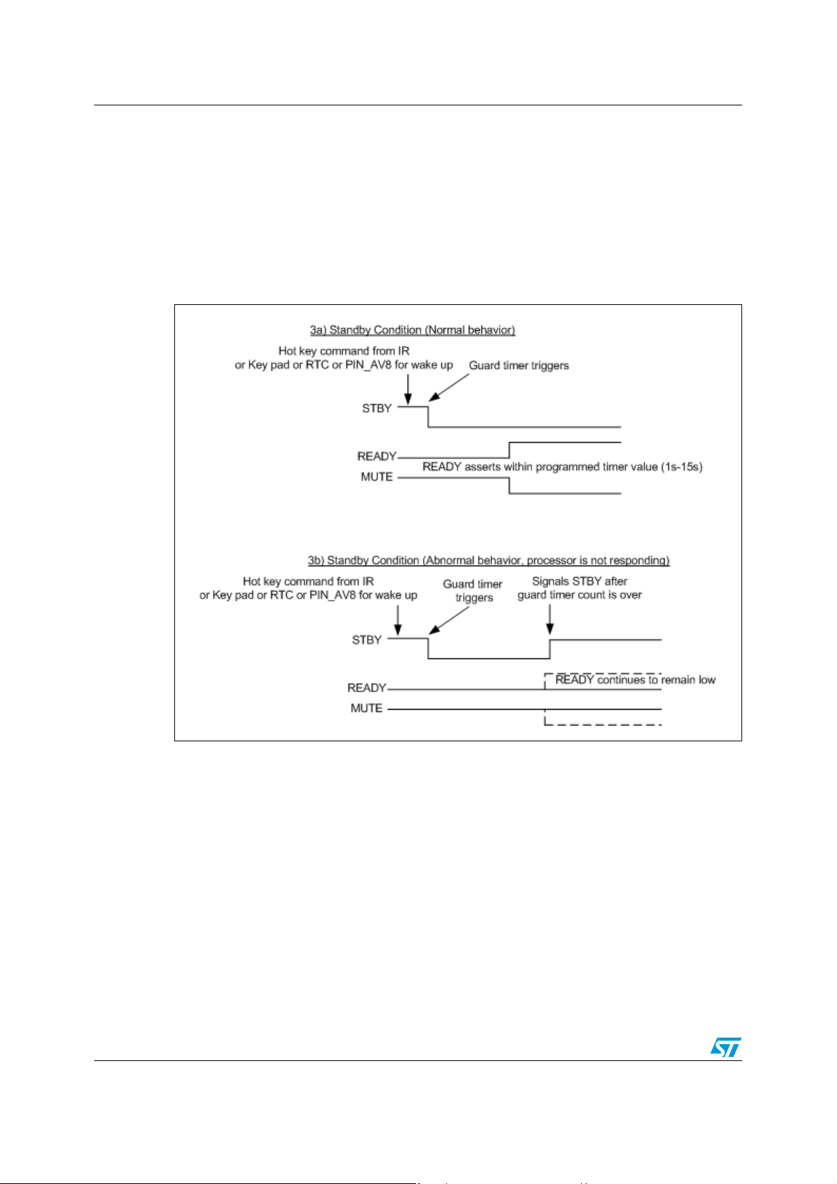
The STFPC320 can wake-up f rom any one of the fo llowing sources:
● Front-panel keys
● Remote-control keys
● Real-time clock (RTC) in 3 conditions (alarm, watchdog timer, oscillator fail)
● External pin PIN_AV8 (only by a low-to-high transition on this pin)
Figure 6. Wake-up
Note: 1 When the hot-key is detect ed either fr om front-pane l or remote cont rol or RTC or from a low-
to-high transition on PIN_AV8 pin during standby, the STBY pin de-asserts.
2 The de-assertion of the STBY triggers the guard timer.
3 The timer value is the progr am med value by the user (1-1 5s). If t he u ser did not chan ge the
value before entering standby, then it remains 10s.
4 Also note that the guard timer is off when the STFPC320 is in the standby mode.
Guard timer is thus triggered by a de-assertion of the STBY signal or by internal power on
reset signal.
16/78
Page 17
STFPC320 Functional description
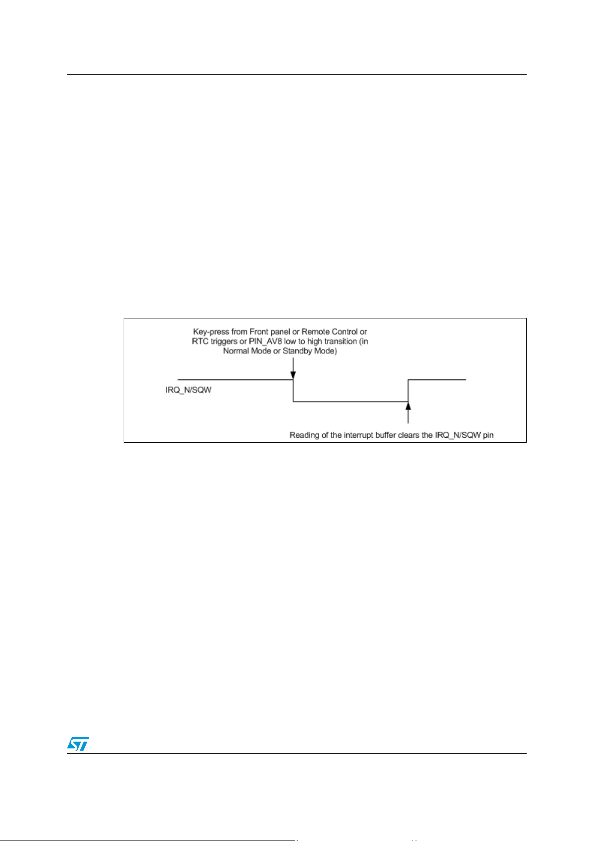
4.5 Interrupts/events handling by STFPC320
The STFPC320 interrupts the Host by pulling the IRQ_N/SQW pin to a low-level both in
normal mode of operation and during wak e-up . The int errupt is enable d by ST FPC320 when
any of the conditions occur:
● Front panel key press in normal operation or during system standb y state
● Remote control key press in normal operation or during system standby state
● A low-to-high transition on the external pin, PIN_AV8
● Real-time clock triggers (alarm, watchdog timer, oscillator fail)
The IRQ_N/SQW is an active low level signal and is cleared only after the interrupt b u ffer is
read. After reading the interrupt buffer, the Host will know the actual source of the interrupt.
This allows the Host to exact ly kno w the event which caused the interrupt (e.g STBY key on
the front panel). The interrupt signal is used to inf orm the Host of any events detected by the
STFPC320. Note that the IRQ_N/SQW pin is an open-drain pin which requires an external
pull-up resistor.
Figure 7. Interrupts/events handling
4.6 Ready pin
The STFPC320 supports cutting-off power to the main board for standby operation for good
power management. STBY will be set to high when the READY transitions from high to low.
During a cold boot up or wakeup from standby, if the READY pin stays low, the STFPC320
will assert the STBY when the guard timer has finished counting down to 0.
When the READY drops to a low, MUTE goes high immediately and soon after (2 µs) the
STBY is asserted.
In the normal mode of operation, when READY is a high, the STBY is asserted only when
the guard timer is enabled and has finished counting down to 0. This is meant to put the
system into standby as the READY pin was stuck at high and the guard timer regi ster was
not cleared before it finished counting down to 0. It is advised to disable the guard timer
during normal operation.
17/78
Page 18

Functional description STFPC320
4.7 Mute pin
The MUTE pin is set to logic high to mute the audio output before power is cut to the host
processor. In wakeup mode, the MUTE pin is set to logic low to enable the audio output
immediately after the high assertion of the READY pin. In general, MUTE f ollows READY pin
with an inverted polarity. This pin is used to prevent pop-up sound during power-up and
power-down states.
4.8 Keyscan matrix/front panel keys
The key scan matrix on the STFPC320 helps to pass command from the front panel to the
host processor through the SDA pin on STFPC320. The STFPC320 can be prog r a mme d to
wake-up the system from standby using any of the 24 keys pressed on the front panel.
These wake-up keys are also referred to as hot-keys.
4.9 LED ports
4 LED displays are supported by the STFPC320. Turning on or off of the LED is done by
issuing write command to the LED port. After reset, the LEDs are off. Note that the LED
outputs sink the current, so the cathode of the diode must be connected to the LED pins of
STFPC320.
4.10 Display
The display is divided into two sections, Normal and real-time clock (RTC).
4.10.1 Normal display
The VFD display is configurable for displays from 8 digits/20 segments to 16 digits/12
segments. The VFD displa y can be configured to be eith er in the normal VFD mode or in the
RTC mode. In the normal VFD mode, the display shows whatever is written in the VFD
display memory.
If the user desires to show normal display simultaneously with the RTC, then CPU must
read the time of RTC display memory and then write all the data to be displayed to the
normal display memory. After writing the values to the display memory, a display-on
command will show both the normal and RTC display on the front panel.
On first power on, the default configuration is 16-digit, 12-segment mode (with display
turned OFF).
4.10.2 RTC display
In RTC mode, th e display can be configured to show the time in two modes, either by dire ct
mapping of RTC to t he display or by using the CPU. If CPU is used, the CPU reads th e R T C
value from RTC registers and then writes the time to be displayed in the RTC display
memory.
18/78
Page 19

STFPC320 Functional description
4.11 Remote control decoder
Remote control (RC) decoder module decodes the signal coming from IR_DATA_IN. The list
of IR remote control protocols recognized by STFPC320 is Philips RC-5, SONY, NEC,
Thomson-RCA, Thomson-R2000 and Matsushita. The selection of remote control protocol
to use is done by setting the RC Protocols register. The commands from RC is used to
wake-up from standb y and resume n ormal operation. All RC ke ys can be pro grammed t o act
like RC hotkeys. Upon receiving any one of the designated hotkeys, wake-up operation will
begin.
4.12 PIN_AV8
External device (e.g. set-top box) could pull this pin high to wake-up the system. A low-to-
high transition on this pin will signal the STPFC320 to wake-up and provide power to the
system. This signal is considered high when it is in the range of 2.5 - 3.6 V (proper voltage
division must be done externally so that the STFPC320 PIN_ AV8 sees no more than 3.6 V).
No action is taken on the high-to-low transition on PIN_AV8. Also when the pin is already a
high, the current state of the system is maintained and it does not trigger anything.
4.13 Default state upon power-up
The Table 3 below shows the default state of the STFPC320 upon power-up.
Table 3. Default state
S.No. Functions Default state
1 Display OFF
2Key-scan ON
3 IR (Remote Control) ON
4 Display mode 12 segment/16 digit
5 Display address 10H with Address increment mode
6 RC protocol RC-5 (Raw format)
7LED OFF
8 Dimming 1/16 duty factor
9 Hot Keys (IR and FP) Disabled
10 Guard timer 10s
19/78
Page 20

Functional description STFPC320
4.14 Initial state
On power application, the 1/16-pulse width is set and th e display shows the value
configured in the VFD display RAM before entering the standby mode. Thus if HELLO is
required to be shown on the VFD upon w ak e-up , then the user must write the cor responding
digit and segments locations in the VFD displa y memory before going in to the standby mo de
of operation. Note that t he V
value of the display changes only after user configuration.
If the user wishes to display t he RTC value during standby, then the user must configure the
STFPC320 by sending the appropriate command. If the user does not configure the
STFPC320 to display the RTC in standby, the VFD shows the same value as was written in
the VFD display memory location.
Note that all the hot keys are disabled on power-up. Only the hotkeys (FP or RC) or RTC or
the low to high transition on the PIN_AV8 pin can be detected to wake-up the system from
standby condition.
must be present in order to keep th e VFD displa y activ e . The
SS
20/78
Page 21
STFPC320 Operating state diagram
5 Operating state diagram
Figure 8. Operating state diagram
21/78
Page 22

Real-time clock (RTC) operation STFPC320
6 Real-time clock (RTC) operation
6.1 Real-time clock
The RTC operates as a slave device through the slave address of the STFPC320 on the
serial bus. Access is obtained by implementing a start condition followed by the correct
slave address (Write: 0x52H and Read: 0x53H). The 16 bytes contained in the device can
then be accessed sequentially in the following order:
1. Reserved
2. Seconds register
3. Minutes register
4. Hours register
5. Square wave/day register
6. Date register
7. Century/month register
8. Year register
9. Calibration register
10. Watchdog register
11 - 15. Alarm registers
16. Flags register
6.2 2-wire bus characteristics
The bus is intended for communication between different ICs. It consists of two lines: a
bidirectional data signal (SDA) and a clock signal (SCL). Both the SDA and SCL lines must
be connected to a positive supply voltage (typical voltage is 3.3 V) via a pull-up resistor
(typical value is 10 K). The following protocol has been defined:
● Data transfer may be initiated only when the bus is not busy.
● During data transfer, the data line must remain stable whenever the clock line is High.
● Changes in the data line, while the clock line is High, will be interpreted as control
signals.
Accordingly, the following bus conditions have been defined:
● Bus not busy: both data and clock lines remain High.
● Start data transfer: a change in the state of the data line, from high to Low, while the
clock is High, defines the START condition.
● Stop data transfer: a change in the state of the data line , from Low to High, while the
clock is High, defines the STOP condition.
● Data Valid: the st ate o f the data line represent s v a lid data when after a sta rt condition,
the data line is stable fo r the durat ion of the high period of the clo ck signal. The data on
the line may be changed during the Low pe riod of the clock signal. There is one clock
pulse per bit of data.
Each data transfer is initiated with a start condition and terminated with a stop
22/78
Page 23
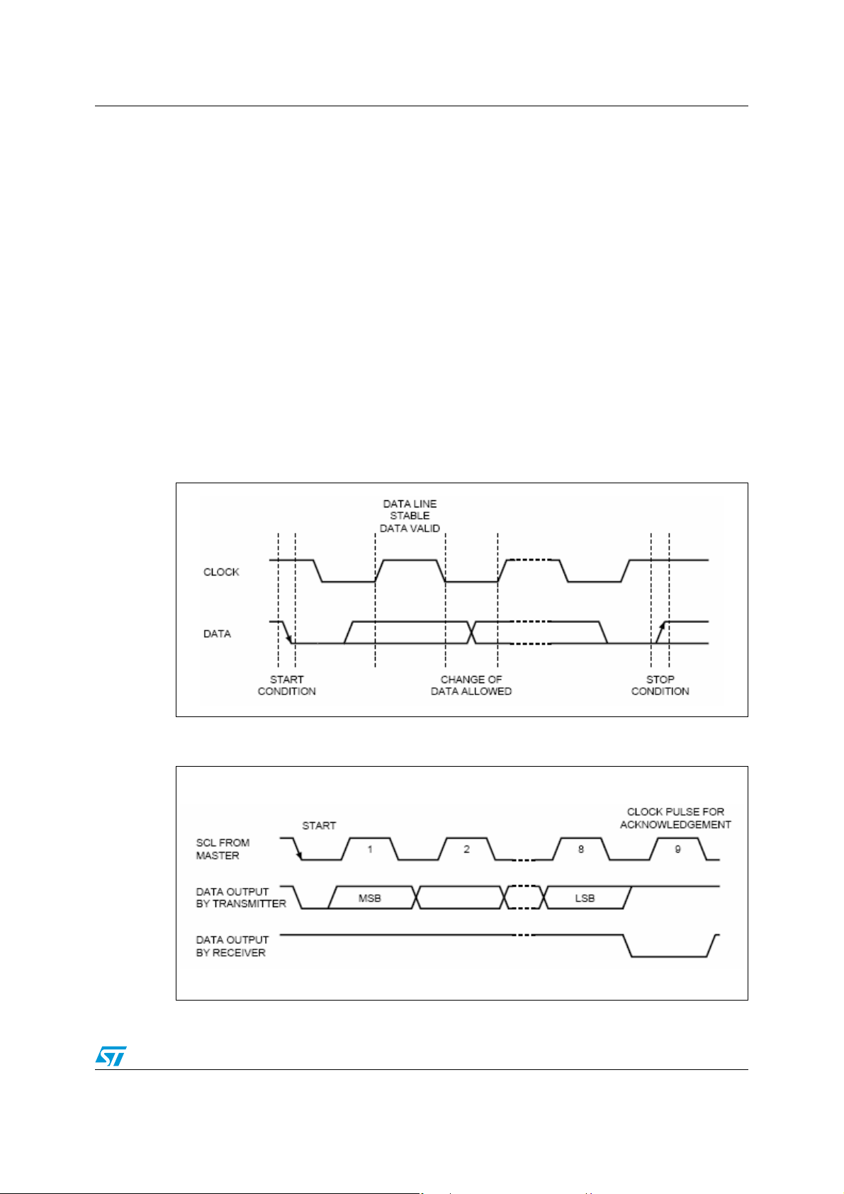
STFPC320 Real-time clock (RTC) operation
condition. The number of data bytes transferred between the start and stop conditions
is not limited. The information is transmitted byte-wide an d each receiver ac knowledges
with a ninth bit.
By definition a device that gives out a message is called “transmitter,” the receiving
device that gets the message is called “recei v er.” The de vice t hat controls t he message
is called “master.” The devices that are co ntrolled by the master are called “sla ves.”
● Acknowledge: each byte of eight bits is followed by one Acknowledge Bit. This
Acknowledge Bit is a low level put on the bus by the receiver whereas the master
generates an extra acknowledge related clock pulse. A slave receiver which is
addressed is obliged to generate an acknowledge afte r the reception of each byte that
has been clocked out of the master transmitter.
The device that acknowledges has to pull down the SDA line during the acknowledge
clock pulse in such a way th at the SD A line is a stable Lo w during the High period of the
acknowledge related clock pulse. Of course, set up and hold times must be taken into
account. A master receiver must signal an end of data to the slave transmitter by not
generating an acknowledge on the last byte that has been clocked out of the slave. In
this case the transmitter must lea v e t he data line High to enab le the master t o gener ate
the STOP condition.
Figure 9. Serial bus data transfer sequence
Figure 10. Acknowledgement sequence
23/78
Page 24

Real-time clock (RTC) operation STFPC320
6.3 Watchdog timer
The watchdog timer can be used to detect an out of control microprocessor. The user
programs the watchdog timer by setting the desired amou nt of time-out into the Watchdog
Register, address 09h. Bits BMB4-BMB0 store a binary multiplier and the three bits RB2-
RB0 select the resolution where:
● 000 = 1/16 second (16Hz)
● 001 = 1/4 second (4Hz)
● 010 = 1 second (1Hz)
● 011 = 4 seconds (1/4Hz)
● 100 = 1 minute (1/60Hz)
Note: Invalid combinations (101, 110, and 111) do NOT enable a watchdog time-out. Setting the
BMB4-BMB0 = 0 with any combination of RB2-RB0, other than 000, will result in an
immediate watchdog time-out. The amount of time-out is then determined to be the
multiplication of the five-bit multiplier value with the resolution. (For example: writing
00001110 in the Watch dog reg ist er = 3*1 or 3 second s). If the pro ces so r do es not reset th e
timer within the specified period, the STFPC320 generates a watchdog output pulse on the
IRQ_N/SQW pin.
The watchdog timer can only be reset b y having the microprocessor perf orm a WRITE of the
Watchdog register. The time-out period then starts over. Should the watchdog timer time-
out, any value may be written to the Watchdog Register in order to clear the IRQ_N/SQW
pin. A value of 00h will disable the watchdog function until it is again programmed to a new
value. A READ of the Flags Register will reset the W atchdog flag (Bit D7; Register 0Fh). The
watchdog function is automatically disabled upon power-up, and the Watchdog Register is
cleared.
6.4 Real-time clock (RTC)
The RTC keeps track of the date and time. Once the date and time are set, the clock works
when the STFPC320 is in normal operation and standby operation. The wake-up alarm
feature is included in the RTC module. The accuracy of the RTC is approximately 10 ppm
(±25 secs/month).
The wakeup alarm is programmed to wake up once the date and time set are met. This
feature is present in normal and standby mode of operation. Only one date and time is
available for setting.
The real-time clock (RTC) uses an external 32.768 kHz quartz crystal to maintain an
accurate internal representation of the second, minute, hour, day, date, month, and year.
The RTC has leap-year correction. The clock also corrects for months having fewer than 31
days.
24/78
Page 25

STFPC320 Real-time clock (RTC) operation
6.4.1 Reading the real-time clock
The real-time clock (R TC) is read by specifying the address correspondin g to the r egist er of
the real-time clock and then initiating a Read command. The RTC registers can then be
read in a sequential read mode. Since the clock runs continuously and a read takes a finite
amount of time, there is the possibility that the clock could change during the course of a
read operation. In this device, the time is latched by the read command (falling edge of the
clock on the ACK bit prior to RTC data output) into a separate latch to avoid time changes
during the read operation. The clock cont inues to run. Alarms occurring during a read are
unaffected by the read operation.
6.4.2 Writing to the real-time clock
The time and date may be set b y writing to t he R TC r egisters . To av oid ch anging th e current
time by an uncompleted write operation, the current time value is loaded into a separate
buffer at the falling edge of the clock on the ACK bit before the RTC data input bytes, the
clock continues to run. The new serial input data replaces the values in the buff er. This new
RTC value is loaded back into the RTC register by a stop bit at the end of a valid write
sequence. An invalid write operation aborts the time update procedure and the contents of
the buffer are discarded. After a valid write operation the RTC will reflect the newly loaded
data beginning with the next “one second” clock cycle after the stop bit is written. The RTC
continues to update the time while an RTC register write is in progress and the RTC
continues to run during any nonvolatile write sequences. A single b yte may be written to the
RTC without affecting the other bytes.
25/78
Page 26

Real-time clock (RTC) operation STFPC320
6.5 Register table for RTC
Table 4. Register table for RTC
Addr D7 D6 D5 D4 D3 D2 D1 D0 Function/range BCD format
00h Reserved Reserved - -
01h ST 10 seconds Seconds Seconds 00-59
02h OFIE 10 minutes Minutes Minutes 00-59
03h 0 0 1 0 hours Hours (24-hour format) Hours 00-23
04h RS3 RS2 RS1 RS0 0 Day of week Day 01-7
05h 1 0 10 date Date: day of month Date 01-31
06h CB0 CB1 0 10M Month Century/month 0-3/01-12
07h 10 Years Year Year 00-99
08h 1 0 S Calibration Calibration
09h RB2 BMB4 BMB3 BMB2 BMB1 BMB0 RB1 RB0 Watchdog
0Ah AFE SQWE 1 Al 10M Alarm month Al month 01-12
0Bh RPT4 RPT5 Al 10 date Alarm date Al date 01-31
0Ch RPT3 0 Al 10 Hour Alarm Hour Al hour 00-23
0Dh RPT2 Alarm 10 minutes Alarm minutes Al min 00-59
0Eh RPT1 Alarm 10 seconds Alarm seconds Al sec 00-59
0Fh WDF AF 0 0 0 Flags
Keys: S = sign bit
ST = stop bit
OFIE = oscillator fail interrupt enable bit
BMB0 – BMB4 = watchdog multiplier bits
CEB = century enable bit
CB = century bit
OUT = output level
AFE = Alarm flag enable flag
RS0-RS3 = SQW frequency bits
RB0 – RB2 = watchdog resolution bits
RPT1 – RPT5 = alarm repeat mode bits
WDF = watchdog flag (read only)
AF = alarm flag (read only)
OF = Oscillator fail bit
SQWE = square wave enable bit
It is recommended to fill the unused bits in the register map to ‘0’ upon a cold boot up.
26/78
Page 27

STFPC320 Real-time clock (RTC) operation
6.6 Setting alarm clock registers
The address locations 0Ah-0Eh contain the alarm settings. The alarm can be configured to
go off at a prescribed time on a specific month, date, hour, minute, or second or repeat
every year, month, day, hour, minute, or second. It can also be programmed to go off while
the STFPC320 is in the standby mode to serve as a system wake-up call.
The bits RPT5-RPT1 put the alarm in the repeat mode of operation. Table 5 shows the
possible configurations . Codes not list ed in the ta ble def ault to the once p er second mode to
quickly alert the user of an incorrect ala rm setting.
When the clock information matches the alarm clock sett ings based on the match criteria
defined by RPT5-RPT1, the AF (Alarm Flag) is set. If AFE (alarm flag enable) is also set
(and SQWE is '0.'), the alarm condition activates the IRQ_N/SQW pin.
Note: Note that by default, the alarm repeat mode is enabled and by default the repeat fre quency
is set to “once per year”.
Note: If the address pointer is allow ed to increment to the flag re gister address , an alarm condition
will not cause the Interrupt/Flag to occur until the address pointer is moved to a different
address. It should also be noted that if the last address written is the “Alarm Seconds,” the
address pointer will increment to the Flag address, causing this situation to occur.
The IRQ_N/SQW output is cleared b y a READ to the f lags register as sho wn in Figure 11. A
subsequent READ of the flags register is necessary to see that the value of the alarm flag
has been reset to '0’.
Figure 11. Alarm interrupt reset waveform
Table 5. Alarm repeat modes
RPT5 RPT4 RPT3 RPT2 RPT1 Alarm se ttings
1 1 1 1 1 Once per second
1 1 1 1 0 Once per minute
1 1 1 0 0 Once per hour
1 1 0 0 0 Once per day
1 0 0 0 0 Once per month
0 0 0 0 0 Once per year
Note: The “Once Per Year” is the default.
27/78
Page 28

Real-time clock (RTC) operation STFPC320
6.7 Calibrating the clock
The STFPC320 is driven by a quartz controlled oscillator with a nominal frequency of
32.768 kHz. The accuracy of the RTC depends on the frequency of the quartz crystal that is
used as the time-base for the RTC. The accuracy of the clock is dependent upon the
accuracy of the crystal, and the match between the capacitive load of the oscillator circuit
and the capacitive load for which the crystal was trimmed. The STFPC320 crystal is
designed for use with a 6 pF crystal load capacitance. When the calibration circuit is
properly employed, accuracy improves to better than ±2 ppm at 25 deg C.
The oscillation rate of crystals changes with temperature. Therefore, the STFPC320 design
employs periodic counter correction. The calibration circuit adds or subtracts counts fro m
the oscillator divider circuit at the divide by 256 stage. The number of times pulses which are
blanked (subtr acted, negat ive calib ration) or split (added, p ositive calibration) depends upon
the value loaded into the five calibration bits found in the calibration register. Adding counts
speeds the clock up, subtracting counts slows the clock down.
The calibration bits occup y the five lower or der bit s (D4- D0 ) in th e calibration register (08h).
These bits can be set to represent any value between 0 and 31 in binary form. Bit D5 is a
sign bit; ‘1’ indicates positive calibration and ‘0’ indicates negative calibration. Calibration
occurs within a 64-minute cycle. The first 62 minutes in the cycle may, once per minute,
have one second either shortened by 128 or lengthened by 256 oscillator cycles . If a binary
‘1’ is loaded into the register, only the first 2 minutes in the 64 minute cycle will be modified;
if a binary 6 is loaded, the first 12 will be affected, and so on.
Therefore, each calibration step has the effect of adding 512 or subtracting 256 oscillator
cycles for every 125,829,120 actual oscillator cycles, that is +4.068 or -2.034 PPM of
adjustment per calibration step in the calibration register.
Assuming that the oscillator is running at exactly 32.768 KHz, each of the 31 increments in
the calibration byte w ould repre sent +10.7 or - 5.35 seconds per day which corresponds to a
total range of +5.5 or -2.75 minutes per month.
Two methods are available for ascertaining how much calibration a given STFPC320 may
require:
● The first involves setting the clock, letting it run for a month and comparing it to a known
accurate reference and recor ding deviation over a fixed period of time. Calibration
values, including the number of seconds lost or gained in a given period allows the
designer to give the end user the ability to calibrate the clock as the environment
requires, e v en if the fina l product is pac kaged in a non-user serviceable en closure . The
designer could provide a simple utility that accesses the calibration byte.
● The second approach is better suited to a manuf acturing environment, an d inv olve s the
use of IRQ_N/SQW pin. This pin will toggle at 512Hz when RS3 = ‘0’, RS2 = ‘1’, RS1 =
‘1’, RS0 = ‘0’, SQWE = ‘1’ and ST = ‘0’. In normal mode, it is always advised to keep the
SQWE to a ‘0’.
Any deviation from 512 Hz indicates the degree and direction of oscillator frequency shift at
the test temperature. For example, a reading of 512.010124 Hz would indicate a +20ppm
oscillator frequency error, requiring a -10 (XX001010) to be loaded into the Calibration Byte
for correction. Note that setting or changing the calibration b yte does not affect the
frequency test or square wave output frequency.
28/78
Page 29

STFPC320 Real-time clock (RTC) operation
Figure 12. Crystal accuracy across temperature
Figure 13. Calibrating waveform
29/78
Page 30

Real-time clock (RTC) operation STFPC320
6.8 Square wave output
The STFPC320 offers t he user a progr ammab le square w av e function which is output on the
IRQ_N/SQW pin. RS3-RS0 bits located in 04h register establish the square wave output
frequency. These frequencies are listed in Table 6. Once the selection of the SQW
frequency has been completed, the IRQ_N/SQ W pin can be turned on or off under sof tw are
control with the square wav e enab le bit (SQWE) located in reg ister 0Ah. The initial po wer-up
default for the IRQ_N/SQW output is 32 KHz.
Table 6. Square wave output frequency
Square wave bits Square wave
RS3 RS2 RS1 RS0 Frequency Units
0000None-
000132.768kHz
00108.162kHz
00114.096kHz
01002.048kHz
01011.024kHz
0110512Hz
0111256Hz
1000128Hz
100164Hz
101032Hz
101116Hz
11008Hz
11014Hz
11102Hz
11111Hz
30/78
Page 31

STFPC320 Real-time clock (RTC) operation
6.9 Century bits
These two bits will increment in a binary fashion at the turn of the century, and handle all
leap years correctly. See Table 7 below for additional explanation.
Table 7. Century bits
CB1 CB0 Leap Year? Example
0 0 Yes 2000
0 1 No 2100
1 0 No 2200
1 1 No 2300
1. Leap year occurs every four years (for years evenly divisible by 4), except for years evenly divisible by
100. The only exceptions are those years evenly divisible by 400 (the year 2000 was a leap year, year
2100 is not).
(1)
6.10 Oscillator stop detection
If the oscillator fail (OF) bit is internally set to a ‘1’, this indicates that the oscillator has either
stopped, or was stopped f or some period of time a nd can be used to judge the v alid ity of the
clock and date data. This bit will be set to ‘1’ any time the oscillator stops.
In the event the OF bit is found to be set to ‘1’ at any time other than the initial power-up, the
STOP bit (ST) should be written to a ‘1’, then immediately reset to a ‘0’. This will restart the
oscillator.
The following conditions can cause the OF bit to be set:
● The first time power is applied (defaults to a ‘1’ on power-up).
Note: If the OF bit cannot be written to ‘1’ four (4) seconds after the initial power-up, the STOP bit
(ST) should be written to a ‘1’, then immediately reset to a ‘0’.
● The voltage present on Vcc is insufficient to support oscillation.
● The ST bit is set to a ‘1’.
● External interference of the crystal
If the oscillator fail interrupt enable bit (OFIE) is set to a ‘1’, the IRQ_N/SQW pin will also be
activated. The IRQ_N/SQW output is cleared by resetting the OFIE or OF bit to ‘0’ (NOT by
reading the Flag register).
The OF bit will remain set to ‘1’ until written to logic ‘0’. The oscillator must start and have
run for at least 4 seconds before attempting to reset the OF bit to ‘0’. If the trigger event
occurs during the power-down condition, this bit will be set correctly.
31/78
Page 32

Real-time clock (RTC) operation STFPC320
6.11 Initial power-on defaults
Upon application of power to the device, the register bits in the RTC will initially power-on in
the state indicated in Table 8.
Table 8. Initial power-on default values of the registers
ST OF OFIE OUT AFE SQWE RS3-1 RS0 Watchdog
01 0 1 0 0 0 1 0
Note: All other control bits power- up in an undet ermined state. The user sho uld write the OF bit to
a 0 after 4s (after the oscillator has started up and the clock is stable). If the OFIE is to be
enabled, then write a ‘1’ to the OFIE bit in the RTC register.
32/78
Page 33

STFPC320 Commands
7 Commands
A command sets the display mode and status of the VFD driver.
The first 1 byte input to the STFPC320 through the SDA pin after the slave address is
regarded as a command. If slave address is not transmitted before the commands/data are
transmitted, the commands/data being transmitted are invalid (howev er , the commands/data
already transmitted remain valid).
7.1 Configuration mode setting command
This command initializes the STFPC320 and performs any one of the following functions:
1. Selects the number of segments and num ber of g rids (1/8 to 1/16 duty, 12 segments to
20 segments). When this command is executed, display is turned off. To resume
display, the display ON command must be executed. If the same mode is selected,
nothing is performed.
2. Selects the remote control protocol to use.
3. Sets the guard timer. The guard timer is configurable from 1 to 15s or turned off
completely.
4. Sets the guard timer action to perform when the guard timer counts. Two actions are
allowed: no action, set STBY to high level.
MSB LSB
0 0 b5 b4 b3 b2 b1 b0
Description: Bits b7-b6 = 00 is decoded as a configuration mode setting command. The
subsequent bits are decoded as follows:
b5: Reserved
b4: Normal display setting
b3: RTC display setting (during normal or STBY modes)
b2: enables all RC keys as hot-keys
b1: Reserved
b0: enables the guard timer to issue STBY
Note: When displaying the RTC during normal mode, if the µP is writing data to STFPC320 using
2
I
C bus, the RTC display on VFD momentarily turns OFF.
33/78
Page 34

Commands STFPC320
The first byte after the configuration command is in the following format:
Figure 14. First byte format after configuration byte
MSB LSB
MSB LSB
MSB LSB
b0b1b2b3b4b5b6b7
b0b1b2b3b4b5b6b7
b0b1b2b3b4b5b6b7
GUARD TIMER SETTING
GUARD TIMER SETTING
GUARD TIMER SETTING
0000 : Turned off
0000 : Turned off
REMOTE CONTROL PROTOCOL
REMOTE CONTROL PROTOCOL
REMOTE CONTROL PROTOCOL
SETTING
SETTING
SETTING
(Decoded format since b7=‘0’)
(Decoded format since b7=‘0’)
(Decoded format since b7=‘0’)
0110 : R2000
0110 : R2000
0111 : RCA
0000 : RC Disable
0000 : RC Disable
0000 : RC Disable
0010 : RC-5
0010 : RC-5
0010 : RC-5
0011 : Reserved
0011 : Reserved
0011 : Reserved
0100 : NEC
0100 : NEC
0100 : NEC
0111 : RCA
0101 : Sony
0101 : Sony
0001: Matsushita
0001: Matsushita
0000 : Turned off
0001 : 1 seconds
0001 : 1 seconds
0001 : 1 seconds
1111 : 15 seconds
1111 : 15 seconds
1111 : 15 seconds
xxxx : No. of seconds in BCD
xxxx : No. of seconds in BCD
xxxx : No. of seconds in BCD
format
format
format
When b7 = ‘0’, incoming RC data is output on SDA in decoded format where the Device
Address, Start Bit, Toggle Bit and Data Bits are sent. Note that the default location is 0x00
for the first device address. This order of the bits sent is in the same f o rmat as the incoming
RC data.
When b7 = ‘1’, incoming raw data (no header information) is output on SDA.Address
decoding is still performed to decode the corresponding RC protocol. The format of the data
on SDA corresponds to the format of the respective RC f rame.
For details, refer to the RC protocol section of the datasheet.
Upon power application, the following modes are selected:
● Normal display setting: 16-digit, 12-segment mode is selected (default: display off and
keyscan on).
● Remote control protocol setting: RC-5 with raw format.
● Guard timer setting: turned on with 10s. After the fi rst command is processed by
STFPC320, the guard timer is turned off until it is turned on by the host.
● Guard timer action: issue standby.
34/78
Page 35

STFPC320 Commands
The second byte after the configuration command is in the format displayed in Figure 15
Figure 15. Second byte format after configuration type
MSB LSB
MSB LSB
b0b1b2b3b4b5b6b7
b0b1b2b3b4b5b6b7
RTC DISPLAY MODE
RTC DISPLAY MODE
SETTING
SETTING
0000: RTC digit 1 (default)
0000: RTC digit 1 (default)
0001: RTC digit 2
0001: RTC digit 2
0010: RTC digit 3
0010: RTC digit 3
0011: RTC digit 4
0011: RTC digit 4
0100: RTC digit 5
0100: RTC digit 5
0101: RTC digit 6
0101: RTC digit 6
0110: RTC digit 7
0110: RTC digit 7
Note that the RTC digit 1 is the
Note that the RTC digit 1 is the
default setting.
default setting.
VFD DISPLAY MODE SETTING
VFD DISPLAY MODE SETTING
0111 : 8 digits, 20 segments
0111 : 8 digits, 20 segments
1000 : 9 digits, 19 segments
1000 : 9 digits, 19 segments
1001 : 10 digits, 18 segments
1001 : 10 digits, 18 segments
1010 : 11 digits, 17 segments
1010 : 11 digits, 17 segments
1011 : 12 digits, 16 segments
1011 : 12 digits, 16 segments
1100 : 13 digits, 15 segments
1100 : 13 digits, 15 segments
1101 : 14 digits, 14 segments
1101 : 14 digits, 14 segments
1110 : 15 digits, 13 segments
1110 : 15 digits, 13 segments
1111 : 16 digits, 12 segments
1111 : 16 digits, 12 segments
HHMMSS
Dig 1 Dig 2 Dig 3 Dig 4 Dig 5 Dig 6 Dig 7 Dig 8 Dig 9 Dig 10
The above example shows the HH, MM, SS digits on a 10-digit display panel when RTC
digit 1 is configured (Bits b7 - b4= “0000”) & HH:MM:SS format is selected with separator
being a part of the same digit. The MSB of Hour corresponds to Digit 1 when
b7 - b4= “0000”.
When b7-b4=“0001” is configured, the MSB of Hour starts from the Digit 2.
Note: The Digit 1 must start from the left.
35/78
Page 36

Commands STFPC320
7.2 Data setting command
This command sets the data-write and data-read modes.
MSB LSB
0 1 b5 b4 b3 b2 b1 b0
Description: Bits b7-b6 = 01 is decoded as a data setting command. The subsequent bits are
decoded as follows:
b5 b4 = 00: data write command (see bits b1-b0)
b5 b4 = 10: data read 1 command (see bits b1-b0)
b5 b4 = 11: data read 2 command (see bits b1-b0)
b5 b4 = 01: reserved
b3: clear the guard timer (no change in guard time)
b2: ‘1’ implies fixed address of display RAM/ ‘0’ implies auto increments the address
after data has been written.
Table 9. Data write command. b5 b4: 00
b1-b0
00 Write memory (display or RTC) – See Note Note: on page 37
01
10
11 Write LED (see Section 9: LED port on page 44)
Enter Test mode (only used for production test)
Do not use this in normal operatio n.
Clear Test mode
Do not use this in normal operatio n.
Table 10. Data read 1 command. b5 b4: 10
b1-b0
00 Read Key (Section 8: Key matrix on page 42)
01
10
11 Read Interrupt (refer to Section 14: Interrupt flags on page 50)
Read Switch + Address Pointer
(see Section 10: SW data on page 45)
Read RC data (following two bytes are the address + command from
RC); Refer to Section 15: Remote control protocols on page 51
Table 11. Data read 2 command. b5 b4: 11
b1-b0
00 Reserved
01 Read Configuration (see Section 13: Configuration data on page 48)
36/78
Page 37

STFPC320 Commands
Table 11. Data read 2 command. b5 b4: 11
10 Reserved
11
Read RTC Registers
(see Section 11.1: RTC display data read on page 46)
On power application, the normal display mod e and address incremen t mode is set with the
default display memory address set to 10H.
In the auto increment address mode, the address command is sent only once followed by
the data bytes.
Note: This command is seldom used. For writing to memory (normal or RTC), the address se tting
command is sufficient.
37/78
Page 38

Commands STFPC320
7.3 Display control and hotkey setting command
MSB LSB
1 0 b5 b4 b3 b2 b1 b0
Description: Bits b7-b6 = 10 is decoded as a display control and hotkey setting command. The
subsequent bits are decoded as follows:
b5 = 0: sets display control for dimming setting as shown in the table on the next
page.
When b5 = 1, the decoding is based on bits b2-b0 as illustrated below:
b2 b1 b0 = XX1: RC hotkeys and address configuration.
b2 b1 b0 = X1X: front panel hotkeys configuration.
b2 b1 b0 = 1XX: sets the RTC segments loca tion. Refer to the table below for the
configuration.
b4, b3: reserved (the bits can be set to ‘0’)
Note: XXX on the bit values means don’t care. The bits can be set to ‘0’.
RTC segments configuration
Remote control hotkeys
When b5 = 0
b2.b0: Sets dimming quantity.
000: Sets pulse width to 1/16.
001: Sets pulse width to 2/16.
010: Sets pulse width to 4/16.
011: Sets pulse width to 10/16.
100: Sets pulse width to 11/16.
101: Sets pulse width to 12/16.
110: Sets pulse width to 13/16.
111: Sets pulse width to 14/16.
b3: Turns on/off display
0: Display off (key scan
continues)
1: Display on
When b5 = 1
b2 b1 b0: 1XX
This command is followed by
sending 7 bytes of configuration
data for RTC segments (byte1-
6) and format configuration
(byte7).
Read 12.3.1 for details.
When b5 = 1
b2 b1 b0: XX1
Following this command is
16bytes configuration data for 8
RC hotkeys configuration.
Read 12.3.3 for details.
Front panel hotkeys
When b5 = 1
b2 b1 b0: X1X
This command is followed by
sending 3 bytes (24 keys) of
configuration data to set any ke y
as hotkey.
Section : Thus, if the a
Read
segment is located on
segment 1, the bits b3-b0 are
“0000”. If b segment is
located on segment 2, the
bits b3-b0 are “0001” and so
on. on page 39
for details.
MSB Segment b Segment a LSB
BYTE1b7b6b5b4b3b2b1b0
38/78
Page 39
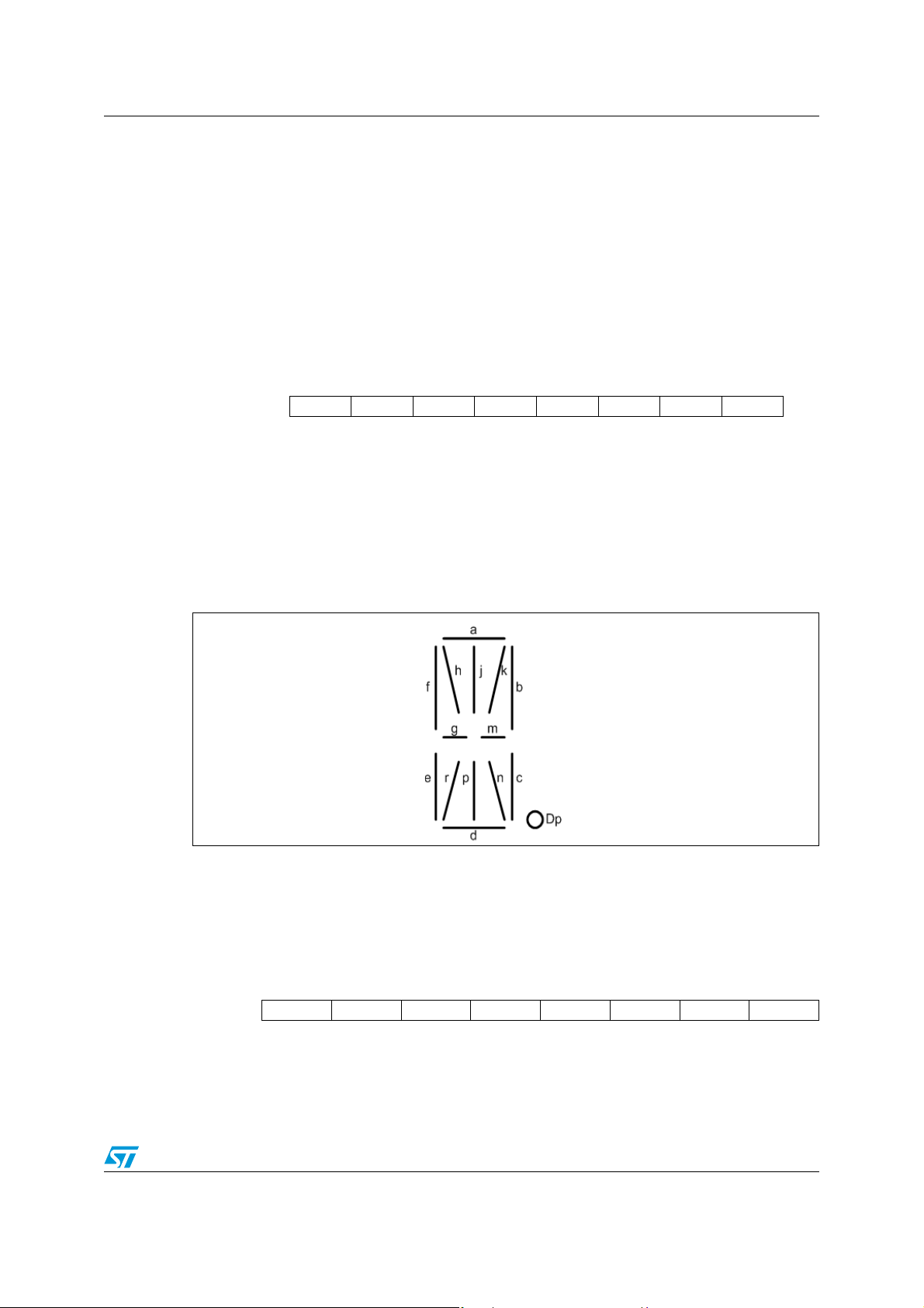
STFPC320 Commands
Description: Byte2 to byte6 will follow the same pattern as shown for byte1 above:
BYTE2: segment d, segment c
BYTE3: segment f, segment e
BYTE4: segment m, segment g
BYTE5: segment k, segment h
BYTE6: segment p/col, segment j/col
Segments r and n are never used for RTC display.
Byte7 is for RTC format configuration:
BYTE7 0 b6 b5 b4 0 0 0 b0
MSB LSB
When b6 is set to a ‘0’, it implies that the dot point/column is a part of the same digit as the
LSB of the HH or LSB of the MM. When b6 is set to a ‘1’, it means that a separate digit is
used for the separator between the hour/minute and minute/second.
When b5 is set to a ‘0’, HH:MM display format of RTC is chosen and when it is set to a ‘1’,
the HH:MM:SS format is chosen.
When b4 is set to a ‘0’, the AM/PM is not displayed and when it is set to a ‘1’, the AM/PM is
displayed on the VFD.
Figure 16. 14-segment + dotpoint display
For a display with segment configuration as in Figure 16, the location of “a” segment
represented by bits b3-b0 corresponds to “0000”. Location of b segment corresponds to
“0001”. Location of c segment correspo nd s to “00 10” an d so on.
Thus, if the a segment is located on segment 1, the bits b3-b0 are “0000”. If b segment is
located on segment 2, the bits b3-b0 are “0001” and so on.
BYTE1 b7 b6 b5 b4 b3 b2 b1 b0
MSB LSB
Description: b0: KS1 KEY1
b1: KS1 KEY2
b2: KS2 KEY1
b3: KS2 KEY2
39/78
Page 40
Commands STFPC320
b4: KS3 KEY1
b5: KS3 KEY2
b6: KS4 KEY1
b7: KS4 KEY2
Byte2 and Byte3 follow the same pattern as above for the hotkey configuration. To
select any one of the key as hotkey, the bit value is set to ‘1’.
Figure 17. Front panel hotkeys configuration
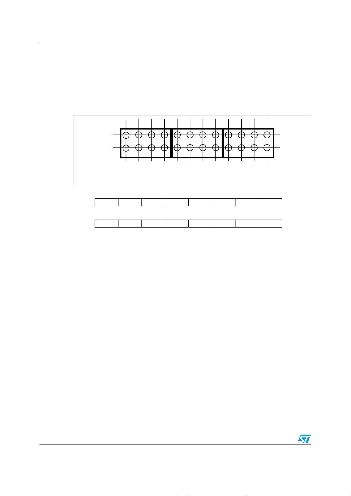
BYTE1 BYTE2 BYTE3
BYTE1 BYTE2 BYTE3
KEY
KEY
KEY
KEY
1
1
1
1
b0
b2 b4
b0
b2 b4
b1 b3
b1 b3
b1 b3
1
1
1
1
/KS
/KS
/KS
/KS
1
1
1
1
Seg
Seg
Seg
Seg
b2 b4
2
2
2
2
/KS
/KS
/KS
/KS
2
2
2
2
Seg
Seg
Seg
Seg
KEY
KEY
KEY
KEY
2
2
2
2
MSB LSB
BYTE1 b7 b6 b5 b4 b3 b2 b1 b0 RC address 1
b5 b7
b5 b7
b5 b7
3
3
3
3
/KS
/KS
/KS
/KS
3
3
3
3
Seg
Seg
Seg
Seg
b6 b0
b6b0
b6 b0
4
4
4
4
/KS
/KS
/KS
/KS
4
4
4
4
Seg
Seg
Seg
Seg
b1 b3
b1 b3
b1 b3
5
5
5
5
/KS
/KS
/KS
/KS
5
5
5
5
Seg
Seg
Seg
Seg
b2 b4
b2 b4
b2 b4
6
6
6
6
/KS
/KS
/KS
/KS
6
6
6
6
Seg
Seg
Seg
Seg
b5 b7
b5 b7
b5 b7
7
7
7
7
/KS
/KS
/KS
/KS
7
7
7
7
Seg
Seg
Seg
Seg
b6 b0
b6b0
b6 b0
8
8
8
8
/KS
/KS
/KS
/KS
8
8
8
8
Seg
Seg
Seg
Seg
b1 b3
b1 b3
b1 b3
9
9
9
9
/KS
/KS
/KS
/KS
9
9
9
9
Seg
Seg
Seg
Seg
b2 b4
b2 b4
b2 b4
10
10
10
10
/KS
/KS
/KS
/KS
10
10
10
10
Seg
Seg
Seg
Seg
b5 b7
b5 b7
b5 b7
11
11
11
11
/KS
/KS
/KS
/KS
11
11
11
11
Seg
Seg
Seg
Seg
b6
b6b0
b6
12
12
12
12
/KS
/KS
/KS
/KS
12
12
12
12
Seg
Seg
Seg
Seg
MSB LSB
BYTE2b7b6b5b4b3b2b1b0RC hotkey 1
Description: To configure an RC hotkey two bytes are required. The first byte is used to specify the
RC address and the second byte is used to specify the hotkey command. Hence
there is the option of having 8 hot ke ys fro m the same RC addr ess or one hotk e y each
for 8 different RC address.
byte1, byte2: RC hotkey1
byte3, byte4: RC hotkey2
byte5, byte6: RC hotkey3
byte7, byte8: RC hotkey4
byte9, byte 10: RC hotkey5
byte11, byte12: RC hotkey6
byte13, byte14: RC hotkey7
byte15, byte16: RC hotkey8
If less than 8 RC hotkeys are required, there is no need to fill all the 16 bytes . The number of
configuration bytes sent will depends on how many hotkeys.
For example , to configure 2 hotkeys from 2 diff erent RC addresses f or Philips RC-5 protocol:
Philips RC-5 Device Address: XXX00001, Hot Key 1: XX000001
Philips RC-5 Device Address: XXX01100, Hot Key 2: XX000010
Note: For RC protocols, where the MSB does not end on the 8-bit, the data is configured starting
from b0 (LSB) to the MSB.
40/78
Page 41

STFPC320 Commands
7.4 Example for device configuration
After the proper power-up se quence, an e xample f or configur ation of the STFPC320 is giv en
below:
1. Configuring display & RC
0x09 = RTC display & enables the guard timer to issue STBY
0xAA = raw format, RC-5 protocol, 10s for initial guard time value
0x0A = digit 1 will show the Hour MSB, 11 digits/17 segments display
2. Configure RTC segments
0xA4 = display control command with RTC segments configuration
0x10, 0x32, 0x54, 0x76, 0xAB, 0xEE = 6 bytes used to map the segment location s for
RTC
0x20 = format of RTC (separator a part of same digit, HH: MM: SS format with no
AM/PM)
3. Configure front panel keys as wake-up keys (hotkeys)
0xA2 = hotkey setting command for front panel keys. Subsequent 3 bytes are used to
configure the desired front panel keys to be wake-up keys as described in Section
Section : Thus, if the a segment is located on segment 1, the b its b3-b0 are “0000”. If b
segment is located on segment 2, the bits b3-b0 are “0001” and so on. on page 39.
4. Configure RC keys as wake-up keys (hotkeys)
0xA1 = hotkey setting command for RC keys. For one hot key configuration from one
RC device address, 2 bytes are sent (1st byte is RC address and 2 byte is hotkey
command as described in Section 7.3 on page 38.
41/78
Page 42

Key matrix STFPC320
8 Key matrix
The key matrix is of 12 x 2 configuration, as shown below.
Figure 18. Key matrix and key-input data storage RAM
KEY
KEY
KEY
1
1
1
KEY
KEY
KEY
2
2
2
2
3
4
5
2
3
2
1
1
1
/KS
/KS
/KS
/KS
/KS
/KS
2
2
2
1
1
1
Seg
Seg
Seg
Seg
Seg
Seg
4
3
4
/KS
/KS
/KS
/KS
/KS
/KS
3
4
3
4
3
4
Seg
Seg
Seg
Seg
Seg
Seg
6
5
6
5
6
7
7
7
/KS
/KS
/KS
/KS
/KS
/KS
/KS
/KS
5
5
5
Seg
Seg
Seg
/KS
6
6
6
7
7
7
Seg
Seg
Seg
Seg
Seg
Seg
The data of each key is stored as illustr ated below and is read by a read command, starting
from the most significant bit.
9
9
9
8
8
8
/KS
/KS
/KS
8
8
8
Seg
Seg
Seg
10
11
10
10
/KS
/KS
/KS
/KS
/KS
/KS
9
9
9
10
10
10
Seg
Seg
Seg
Seg
Seg
Seg
12
11
12
11
12
/KS
/KS
/KS
/KS
/KS
/KS
11
12
11
12
11
12
Seg
Seg
Seg
Seg
Seg
Seg
KEY1..KEY
/KS
Seg
1
Seg5/KS
Seg9/KS
2
1
5
9
KEY1..KEY
Seg2/KS
Seg6/KS
Seg10/KS
2
2
6
10
KEY1..KEY
Seg3/KS
Seg7/KS
Seg11/KS
2
3
7
11
KEY1..KEY
Seg4/KS
Seg8/KS
Seg12/KS
b0---------b1 b2---------b3 b4---------b5 b6---------b7
2
4
8
12
Reading last
Reading first
42/78
Page 43

STFPC320 Key matrix
8.1 Key read sequence
MSB LSB
Data Setting Command01100000
MSB LSB
Key Data Byte 1
Key Data Byte 2
Key Data Byte 3
Description: For example when the key corresponding to the KEY1/KS1 is pressed, the bit b0 of
Byte 3 will be set. This is decoded as the key value connected to KEY1/KS1 which
could be “PLAY” (for example). When the processor decodes the key value
corresponding to the “PLAY” key, it takes the necessary action (e.g. play the disc).
b7 b6 b5 b4 b3 b2 b1 b0
MSB LSB
b7 b6 b5 b4 b3 b2 b1 b0
MSB LSB
b7 b6 b5 b4 b3 b2 b1 b0
Note: Upon a key-press, the IRQ_N/SQW pin will be a sserted. The interrupt flag should be read to
know the source of interrupt. The interrupt flag is read by sending the 0x63 command. As
soon as the interrupt buffer is read, the IRQ_N/SQW pin will be de-asserted.
43/78
Page 44

LED port STFPC320
9 LED port
Data is written to the LED port by a write command, starting from the most significant bit of
the port. When a bit of this port is set to 0, the corresponding LED lights up; when the bit is
set to a 1, the LED turns off. The data of bits 5 through 8 are ignored. Upon first power-up,
all the LEDs are turned OFF.
Figure 19. LED byte format
MSB LSB
MSB LSB
b0b1b2b3----
b0b1b2b3----
LED1
LED1
LED2
LED2
LED3
LED3
LED4
LED4
Don’t Care
Don’t Care
9.1 Writing to LED sequence
MSB LSB
Data Setting Command01000011
Data (will turn on all the 4 the LEDs)
MSB LSB
Data Byte XXXX0000
For ex ample, the LEDs can be connected to indicate ‘Power-On’, ‘Standby’, ‘Record’,
‘Function’ status on front panel. If the data bit corresponding to the LED is a ‘0’, the LED will
turn-on during normal operation and standby mode.
So as an example, to turn on the LED for standby indication, the processor must write ‘0’ to
the corresponding data bit before de-asserting the READY pin (i.e. before going into STBY).
This will continuously keep the STBY LED ‘ON’ during standby mode of operation.
44/78
Page 45

STFPC320 SW data
10 SW data
The SW data are read by the appropriate read command, starting from the most significant
bit. Bits 3 through 8 (b7-b2) represent the Address pointer for the internal RAM.
Figure 20. LED byte format
MSB LSB
MSB LSB
b0b1b2b3b4b5b6b7
b0b1b2b3b4b5b6b7
SW1
SW1
SW2
SW2
Address pointer for the memory
Address pointer for the memory
10.1 Reading switch sequence
MSB LSB
Data Setting Command01100001
After sending this command, the STFPC320 will output a byte with the 2 bit values of the 2
switches and 6-bit addres s pointer values.
45/78
Page 46

Address setting command STFPC320
11 Address setting command
This command sets an address of the displa y memory or the address of the RTC register
map.
MSB LSB
01100001
Address (00h - 3Fh)
The address range from 00h -0Fh r ep re sent s the RTC register map. For writing data to RTC
or Normal display registers, address command is sent followed by the RTC or normal
display data.
10h-3Fh represents the normal display memory map. On power application, the default
address location is 10h.
11.1 RTC display data read
When the CPU wants to read the RTC data from the specified memory location of RTC, the
user must first set the address of the RTC location using “address setting command” after
which send the “read RTC register” command.
Thus before reading the RTC register data, the user must set the proper address for R TC
using “address setting command”.
As an example:
Address setting command with RTC memory add re ss of 0x01: 0xC1
Read RTC register command: 0x73
Subsequently STFPC320 will output the data byte from RTC memory location 0x01.
11.2 Display (normal & RTC) data write
The data can be written to the normal or RTC display memory by issuing an address setting
command followed by the data byte s to be written (in auto-increment mode).
As an example, address setting command with normal display memory address of 0x10:
0xC2 subsequently the host can write the data bytes starting from memory location 0x10.
For fixed address mode, the address command has to be sent followed by the display data.
When the next byte of data is to be written, address command has to be sent again before
the new display data byte.
46/78
Page 47

STFPC320 Normal display memory locations
12 Normal display memory locations
Table 12. Display RAM address and display mod e
Seg
1
10 HL 10 HU 11 HL 11 HU 12 HL DIG
Seg
4
Seg
8
Seg
12
Seg
16
Seg
20
1
13 HL 13 HU 14 HL 14 HU 15 HL DIG
16 HL 16 HU 17 HL 17 HU 18 HL DIG
19 HL 19 HU 1A HL 1A HU 1B HL DIG
1C HL 1C HU 1D HL 1D HU 1E HL DIG
1F HL 1F HU 20 HL 20 HU 21 HL DIG
22 HL 22 HU 23 HL 23 HU 24 HL DIG
25 HL 25 HU 26 HL 26 HU 27 HL DIG
28 HL 28 HU 29 HL 29 HU 2A HL DIG
2B HL 2B HU 2C HL 2C HU 2D HL DIG
2E HL 2E HU 2F HL 2F HU 30 HL DIG
31 HL 31 HU 32 HL 32 HU 33 HL DIG
34 HL 34 HU 35 HL 35 HU 36 HL DIG
37 HL 37 HU 38 HL 38 HU 39 HL DIG
3A HL 3A HU 3B HL 3B HU 3C HL DIG
2
3
4
5
6
7
8
9
10
11
12
13
14
15
3D HL 3D HU 3E HL 3E HU 3F HL DIG
b
7 b4b3
XX H
L
XX H
b
0
U
16
Higher 4 bits Lower 4 bits
Only the lower 4 bits of the addresses assigne d to Seg17 through Seg20 are valid, the higher
4 bits are ignored.
Note that the common grid/segment outputs are grid-based. The grid has to be enabled
before any segments can be turned on. If data is written for a segment before enabling the
respective grid, nothing is present on the display.
47/78
Page 48
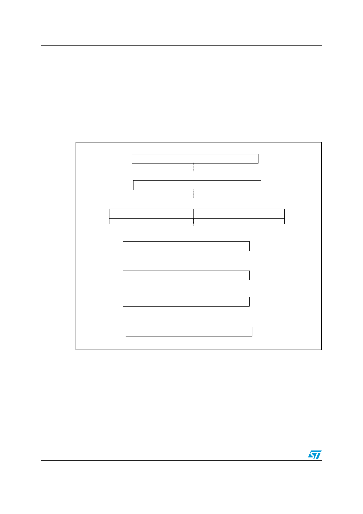
Configuration data STFPC320
13 Configuration data
To read the configuration data from STFPC320, 0x71 command (Section 7.2: Data setting
command on page 36) is sent from the Host to STFPC320. After this, the STFPC320 will
output a maximum of 14 b ytes with the config uration data. T he Host can choose to read only
a few bytes by pulsing the SCL line according to the number of bytes to be read.
Up to a maximum of 14-bytes are sent from MSB to LSB as config uration data. The 14-b ytes
represent the following configuration information.
Figure 21. Configuration data bytes
MSB LSB
MSB LSB
Byte 1
Byte 1
Byte 2
Byte 2
Byte 3
Byte 3
b7 b4 b3 b0
b7 b4 b3 b0
MSB LSB
MSB LSB
b7 b4 b3 b0
b7 b4 b3 b0
MSB LSB
MSB LSB
VFD Dimming and (ON/OFF) status
VFD Dimming and (ON/OFF) status
b7 b4 b3 b0
b7 b4 b3 b0
Clock init display locationNo. of VFD display digits
Clock init display locationNo. of VFD display digits
RC ProtocolGuard Timer Value
RC ProtocolGuard Timer Value
RTC Display format
RTC Display format
Byte 4
Byte 4
Byte 5
Byte 5
Byte 6
Byte 6
Byte 7
Byte 7
MSB LSB
MSB LSB
Front Panel Hot Keys (1stByte)
Front Panel Hot Keys (1stByte)
b7 b0
b7 b0
MSB LSB
MSB LSB
Front Panel Hot Keys (2ndByte)
Front Panel Hot Keys (2ndByte)
b7 b0
b7 b0
MSB LSB
MSB LSB
Front Panel Hot Keys (3rdByte)
Front Panel Hot Keys (3rdByte)
b7 b0
b7 b0
MSB LSB
MSB LSB
RC Device Address 1
RC Device Address 1
b7 b0
b7 b0
48/78
Page 49

STFPC320 Configuration data
Figure 22. Configuration data bytes (continued)
MSB LSB
MSB LSB
Byte 8
Byte 8
Byte 9
Byte 9
Byte 10
Byte 10
Byte 11
Byte 11
Byte 12
Byte 12
b7 b0
b7 b0
MSB LSB
MSB LSB
b7 b0
b7 b0
MSB LSB
MSB LSB
b7 b0
b7 b0
MSB LSB
MSB LSB
b7 b0
b7 b0
MSB LSB
MSB LSB
b7 b0
b7 b0
RC Device Address 2
RC Device Address 2
RC Device Address 3
RC Device Address 3
RC Device Address 4
RC Device Address 4
RC Device Address 5
RC Device Address 5
RC Device Address 6
RC Device Address 6
Byte 13
Byte 13
Byte 14
Byte 14
MSB LSB
MSB LSB
RC Device Address 7
RC Device Address 7
b7 b0
b7 b0
MSB LSB
MSB LSB
RC Device Address 8
RC Device Address 8
b7 b0
b7 b0
49/78
Page 50
Interrupt flags STFPC320
14 Interrupt flags
The interrupt is sent on the IRQ_N/SQW pin when any one of the events occur: FP key
pressed, RC key pressed, PIN_AV8 transitions to a high or RTC events (watchdog timer,
alarm, oscillator fail). Simultaneously, the interrupt flags are set.
The micro-processor can read the interrupt flags by sending the “01100011” command.
After decoding this command, STFPC320 output one byte data as described below to
indicate the source of interrupt.
Figure 23. Interrupt byte format
b7
b6
B
Normal operation
b5
PIN_AV8RCKFPK
PIN_AV8RCKFPK
b4 b3
Preset-
Preset-
value of
value of
RTC or
RTC or
Watchdog
Watchdog
or OFIE
or OFIE
FP hot
FP hot
key
key
b2 b1 b0
RC hot
RC hot
key
key
Wake-up operation
PIN_AV8
PIN_AV8
LSBMS
Preset-
Preset-
value of
value of
RTC or
RTC or
Watchdog
Watchdog
or OFIE
or OFIE
Note: Default value of the register is 00h.
Description: In the normal mode of operation (system is not in standby), the events described
below will cause any of the b4 to b7 bit to be set to 1 and IRQ_N/SQW will be
asserted low:
b4: RTC events
b5: PIN_AV8 transition to High
b6: valid remote control key detection
b7: front panel key detection
Having detected the assertion of IRQ_N/SQW pin, micro-processor should then read
the interrupt buffer to determine the external event causing the interrupt. Once read,
the buffer will be cleared and IRQ_N/SQW is released.
In the wake-up operation (system is in standby), the events described below will
cause any of the b0 to b3 bit t o be se t to 1 an d wakeup occurs (STBY output is se t to
low):
b0: RTC events
b1: PIN_AV8 transition to High
b2: valid remote control hotkeys detection
b3: front panel hotkeys detection
Once wakeup occurs, micro-processor should pull READY to high to indicate to
STFPC320 of a proper boot-up. The STFPC320 will then assert the interrupt to
indicate that an ex ternal event has been occurred. The microprocessor should then
read the interrupt buffer to determine the event causing the wakeup.
When the interrupt is caused by the RTC, the microprocessor should read the RTC
interrupt flag at address 0Fh to determine the specific RTC event: alarm, watchdog
timer of RTC or oscillator fail.
50/78
Page 51

STFPC320 Remote control protocols
15 Remote control protocols
15.1 Decoded and RAW formats
The main difference between decoded and raw remote-control format is that for decoded
format, the STFPC320 sends the RC data only from RC device address matches 0 of the
remote control protocol being used. Whereas for the raw format, the RC data is sent by
STFPC320 from any device address of the particular remote control protocol being used.
If the STFPC320 is used to send RC data in decoded format in normal mode, it is advisable
that the Host configure the STFPC320 to RC-r aw format befor e ent ering the stan dby mode.
This is to allow wakeup from multiple re mote cont rol device addresses of the remote control
protocol (depending on the configuration as outlined in Section : on page 40). In the
decoded RC format, the STFPC320 device wakes up the system from a single device
address.
15.2 Sending IR data on I2C interface
The IR data is sent on the SDA pin of the I2C interface when the microprocessor issues an
IR data read command (0x62, Section 7.2: Data setting command on page 36). The data is
sent in the decoded format or the raw format depending on the user configuration.
In general, the data is sent on SDA pin in byte format with MSB transmitted first as show n in
Figure 24.
Figure 24. IR data format
Byte 1 Byte 2 Byte 3Data word
MSB LSBMSB LSBMSB LSB
51/78
Page 52
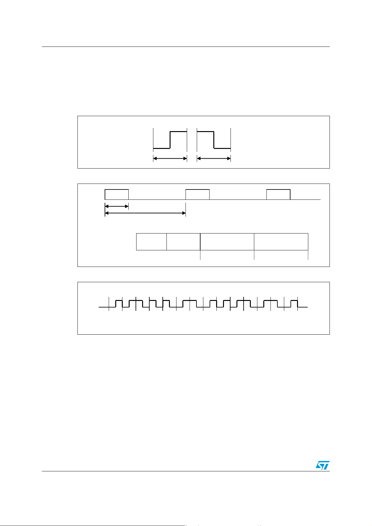
Remote control protocols STFPC320
15.3 Philips RC-5 remote control protocol
The RC-5 remote control protocol is based on bi-phase (aka Manchester) coding as shown
in Figure 25. Note that the coding is on the transmitted side. The dat a on IR_DATA_IN pin of
the STFPC320 after reception by the photo diode will be inverted of below. The MSB is
transmitted first.
Figure 25. Bi-phase coding
Logic 1 Logic 0
1.776ms 1.776ms
Figure 26. RC-5 protocol frame
Data word Data word Data word
24.9 ms
114 ms
Data word
2-bit Start
bits
1-bit
Toggle Bit
5-bit Address 6-bit Command
MSB LSBMSB LSB
Figure 27. Example of RC-5 transmission
1 1 1 1 1 1 1 10 0 0 0 0 011 11 11 11 11 11 11 1100 00 00 00 00 00
For RC 5 data transmission, a binary 1 is represented by a low to high transition and a
binary 0 is represented by a high to low transition from th e IR transmitter.
The first two start bits (S1 and S2 ) are syn c bi ts. For normal operation, they are always set
to “11” on the transmit side. After the photo-diode, there is one inversion. So the data at the
IR_DATA_IN of the STFPC320 will be inverted of above. The next bit is the toggle bit. This
bit is inverted each time a key on the remote control is pressed. Bits A1..A5 are the address
bits. The address bits indicate the intended application that the remote control protocol is
used for. Bits C1..C6 are the command bits. The command bits instruct what action is to be
taken.
52/78
Page 53

STFPC320 Remote control protocols
15.3.1 RC-5 data in decoded format
In the decoded form, the ADR bits followed by Start bit and Toggle Bit followed by Data bits
are sent in this order for each remote control protocol. The number of bits depends on the
corresponding RC protocol. The remaining empty bits are stuffed with 1’s to complete a
byte-aligned data frame.
Example for Philips RC-5 protocol, if the 5-bit ADDR field is “00000” and 6-bit command is
“000001”, the in decoded f ormat the data on SDA pin will be sent as follows with MSB
transmitted first. S stands for Start Bit and T stands for Toggle Bit.
Figure 28. RC-5 data structure in decoded format
Byte 1
Byte 2
Byte 3
15.3.2 RC-5 data in RAW format
In the raw form, the data is sent in the same way as it is received for each RC protocol
except that the header is not transmitted on SD A. So for the above example for Philips RC-5
protocol, the data on SDA pin in raw-format will be as follows:
Figure 29. RC-5 data structure in raw format
Data word
Sent first on SDA
1-bit Start
bit
MSB
1-bit
Toggle Bit
ADR LSB
MSB
0TS00000 0TS00000
LSBDAT
A
XXX10000 XXX10000
XXXXXXXX XXXXXXXX
5-bit Address 6-bit Command
MSB LSBMSB LSB
53/78
Page 54
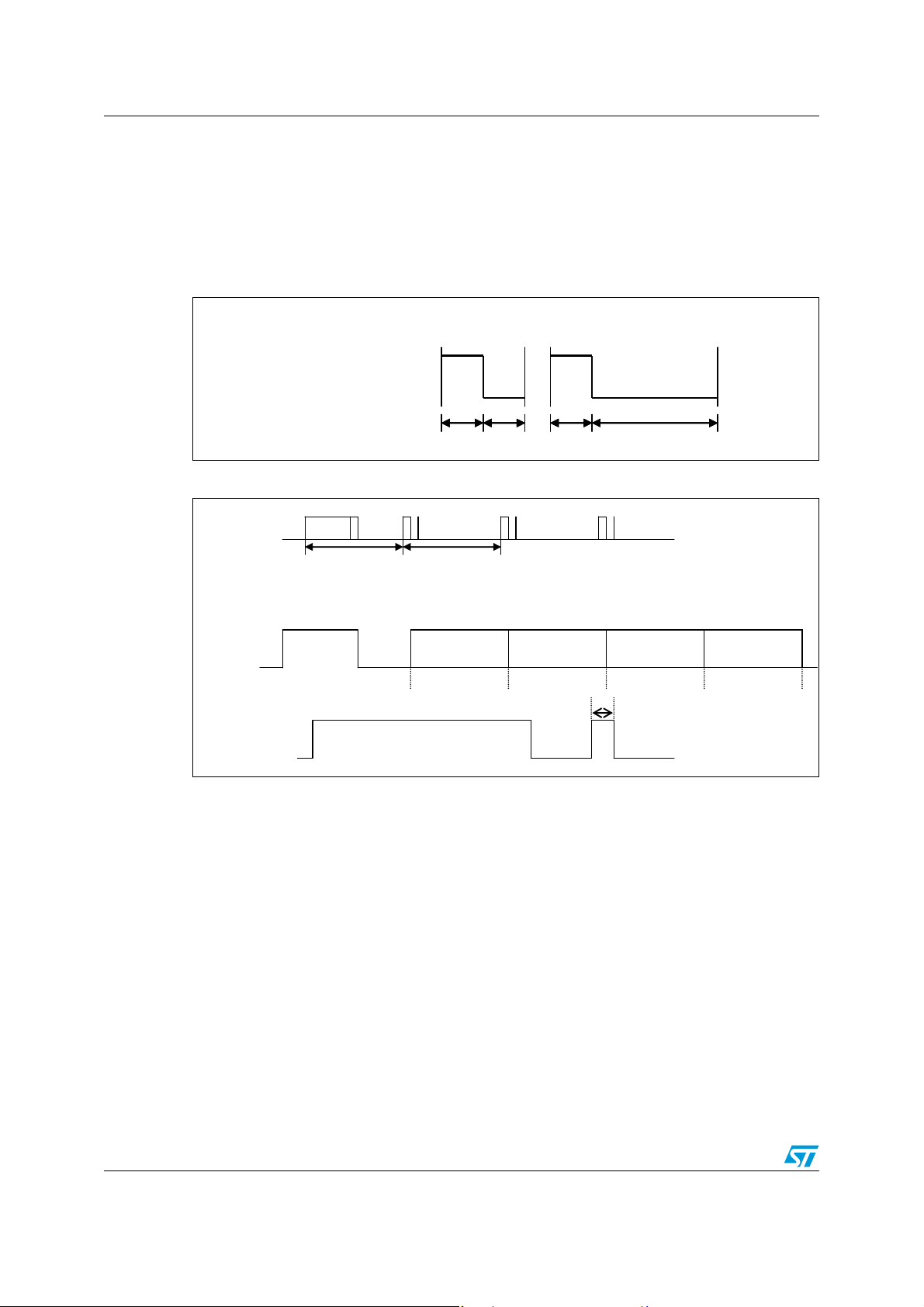
Remote control protocols STFPC320
15.4 NEC remote control protocol
This remote control protocol uses pulse distance modulation. Each bit consists of a high
level of fixed time T, followed by a low level that varies in width. A space that is T represents
a logic “0” and a space that is 3T represents a logic 1. T is 0.56 ms.
The LSB is transmitted first as sho wn in Figure 31.
Figure 30. Pulse distance modulation
Logic 0
Logic 0
T = 0.56 ms
T = 0.56 ms
T
T T3T
T
T T3T
Figure 31. The transmitted waveform for NEC protocol
108 ms 108 ms
First frame Repeat frame
First frame
Repeat frame
9 ms 4.5 ms
8-bit Address
9 ms
Inverted 8-bit
address
2.25 ms
Logic 1
Logic 1
8-bit command Inverted 8-bit
0.56 ms
command
MSBLSBMSBLSBMSBLSB MSBLSB
Note: The above waveform is on the transmitted side. The received data by the STFPC320 after
the photo-diode is inverted from above.
54/78
Page 55
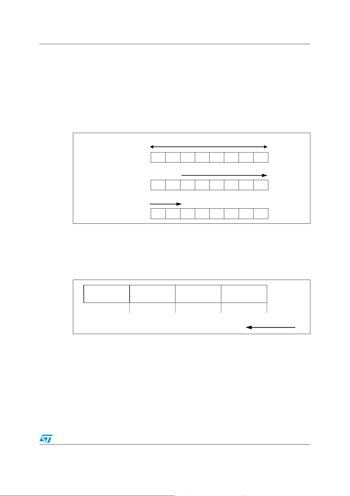
STFPC320 Remote control protocols
15.4.1 NEC in decoded format
In the decoded form, the ADR bits followed by Start bit and Toggle Bit followed by Data bits
are sent in this order for each remote control protocol. The number of bits depends on the
corresponding RC protocol. The remaining empty bits are stuffed with 1’s to complete a
byte-aligned data frame.
Example for NEC protocol, if the 8-bit ADDR field is “00000010” and 8-bit command is
“00011111”, the in decoded format the data on SDA pin will be sent as follows with MSB
transmitted first.
Figure 32. NEC data structure in decoded format
Byte 1
Byte 2
Byte 3
15.4.2 NEC in RAW format
In the raw form, the data is sent in the same way as it is received for each RC protocol
except that the header is not transmitted on SD A. So for the above example for Philips RC-5
protocol, the data on SDA pin in raw-format will be as follows:
Figure 33. NEC data structure in raw format
8-bit Address
MSB LSB
MSB
ADR
DATA
LSB
Inverted 8-bit
address
8-bit command Inverted 8-bit
MSBLSBMSBLSBMSBLSB MSBLSB
01000000 01000000
111000TS 111000TS
XXXXXX11 XXXXXX11
command
Sent first on SDA
55/78
Page 56
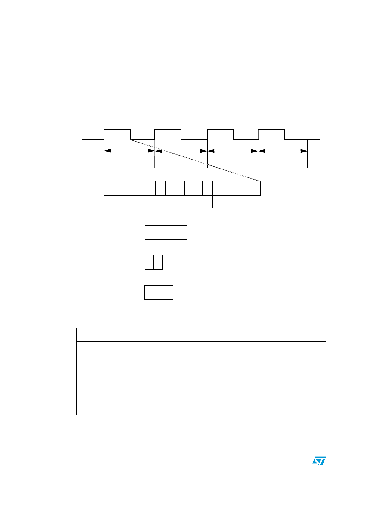
Remote control protocols STFPC320
15.5 Sony remote control format
The modulated carrier is usually derived from 480kHz and is 1/12 of the frequency with 1/3
duty cycle.
When data are transmitted repeatedly, the frame cycle is 45 ms or 150 period.
A frame consists of a syn pulse, a seven-bit data code and a five-bit custom code.
Figure 34. Output code waveform timing definitions
150T
D0 D1
Sym pulse
Sym pulse
150T 150T 150T
D2 D3D4D5
Data code 7 bit
8T
2T 2TData “0”
2T 4TData “1”
Table 13. Sony remote control format
Data item Time (sec) Time (no. of period)
D2 D3 D4 D5
D6
Custom code
D6
5 bit
Syn pulse 2.4ms 8T
Data off time 0.61ms 2T
Data on time (0) 0.59ms 2T
Data on time (1) 1.19 4T
Data on time (0) 1.2 4T
Data on time (1) 1.8 6T
Frame output cycle 45 150T
Note: Where T = 0.3ms
Note that the above waveform is on the transmitted side. The received data by the
STFPC320 after the photo-diode is inverted from above.
56/78
Page 57

STFPC320 Remote control protocols
15.5.1 Sony in decoded format
In the decoded form, the ADR bits followed by Start bit and Toggle Bit followed by Data bits
are sent in this order for each remote control protocol. The number of bits depends on the
corresponding RC protocol. The remaining empty bits are stuffed with 1’s to complete a
byte-aligned data frame.
Example for Sony protocol, if the 5-bit custom code is “11000” and 7-bit data code is
“1010100”, the in decoded format the data on SDA pin will be sent as fo llows with MSB
transmitted first.
Figure 35. Sony data structure in decoded format
Byte 1
Byte 2
Byte 3
15.5.2 Sony in RAW format
In the raw form, the data is sent in the same way as it is received for each RC protocol
except that the header is not transmitted on SDA. If a valid SYN pulse is detected, it is
represented by a bit ‘1’. So a first bit with value ‘1’ implies that the data following it is a valid
raw format RC data. So for the above example for Sony protocol, the data on SDA pin in
raw-format will be as in Figure 36.
Figure 36. Sony data structure in raw format
Sent first on SDA
MSB LSB
ADR
DATA
Data code
7-bit
MSB
1TS00011 1TS00011
LSB
XX001010 XX001010
XXXXXXXX XXXXXXXX
Custom code
5-bit
LSBMSBLSBMSB
57/78
Page 58

Remote control protocols STFPC320
15.6 Matsushita remote control format
The modulated carrier is usually derived from 440 kHz and is 1/12 of the frequency with ½
duty cycle.
When data are transmitted repeatedly, the frame cycle is 104.7 ms or 240 period.
A frame consists of a syn pulse, a five-bit custom code, six-bit data code, a five-bit inverted
custom code and a six-bit inverted data code.
The timing definitions of the output code waveform are shown in Figure 37.
Figure 37. Matsushita remote control protocol
Sym pulse
240T
C0 C1 C2 C3C4 D1 D2 D3 D4 D5
Custom
code 5 bit
Sym pulse
2T 2TData “0”
2T 6TData “1”
2TEnd of transmission
240T 240T 240T
Custom code
5 bit
8T
C’0
C’1
C’0 D’1
C’2C’3C’4
Inverted custom
code 5 bit
8T
D’0
D’2D’3D’4
Inverted data
code 6 bit
D’5
End of transmission
58/78
Page 59
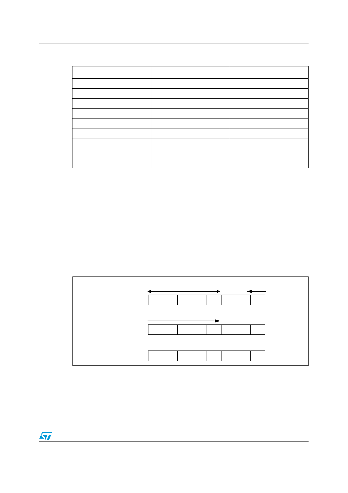
STFPC320 Remote control protocols
Table 14. Matsushita remote control fo rmat
Data item Time (sec) Time (no. of period)
Syn pulse on time 3.49ms 8T
Syn pulse off time 3.49ms 8T
Data on time (0) 0.86ms 2T
Data off time (0) 0.88ms 2T
Data on time (1) 0.86ms 2T
Data off time (1) 2.63ms 6T
Data period (0) 1.74ms 4T
Data period (1) 3.49ms 8T
Frame output cycle 104.7ms 240T
Note: Where T = 0.436 ms
Note that the above waveform is on the transmitted side. The received data by the
STFPC320 after the photo-diode is inverted from above.
15.6.1 Matsushita in decoded format
In the decoded form, the ADR bits followed by Start bit and Toggle Bit followed by Data bits
are sent in this order for each remote control protocol. The number of bits depends on the
corresponding RC protocol. The remaining empty bits are stuffed with 1’s to complete a
byte-aligned data frame.
For Matsushita protoc ol, if the 5-bit custom code is “1100 0” and 6-bit d ata code is “101010 ”,
the in decoded format the data on SDA pin will be sent as follows with MSB transmitted first.
Figure 38. Matsushita data structure in decoded format
MSB LSB
Byte 1
Byte 2
Byte 3
ADR MSB
DATA
LSB
1TS00011 1TS00011
XXX01010 XXX01010
XXXXXXXX XXXXXXXX
59/78
Page 60

Remote control protocols STFPC320
15.6.2 Matsushita in RAW format
In the raw form, the data is sent in the same way as it is received for each RC protocol
except that the header is not transmitted on SDA. If a valid SYN pulse is detected, it is
represented by a bit ‘1’. So a first bit with value ‘1’ implies that the data following it is a valid
raw f ormat RC data. So for the above example for Matsushita protocol, the d ata on SDA pin
in raw-format will be as in Figure 39.
Figure 39. Matsushita data structure in raw format
Custom code
Sent first on SDA
5-bit
Data code
6-bit
Inverted Custom
code 5-bit
LSBMSBLSBMSB LSB LSBMSB MSB
Inverted Data
code 6-bit
60/78
Page 61

STFPC320 Remote control protocols
15.7 R2000 remote control format
Figure 40. Thomson R2000 remote control protocol
1 Dataword = 80 ms
1 Dataword = 80 ms
min. 30.36 ms
min. 30.36 ms
max. 60.72 ms max. 49.64 ms
max. 60.72 ms max. 49.64 ms
2.53 ms 5.06 ms 480 μs
2.53 ms 5.06 ms 480 μs
min. 19.28 ms
min. 19.28 ms
A3 A2 A1 A0 T0 D6 D5 D4 D3 D2 D1 D0 Pause
A3 A2 A1 A0 T0 D6 D5 D4 D3 D2 D1 D0 Pause
modulated mode
modulated mode
(16 pulses)
(16 pulses)
logic 0 = 2.53 ms
logic 0 = 2.53 ms
logic 1 = 5.06 ms
logic 1 = 5.06 ms
A0 – A3 = Address bits (4-bit)
A0 – A3 = Address bits (4-bit)
T0 = Toggle bit
T0 = Toggle bit
D0 – D6 = Command bits (7-bit)
D0 – D6 = Command bits (7-bit)
MSB is sent first.
MSB is sent first.
30 μs
30 μs
33.3 kHz
33.3 kHz
A3
A3
Note: The above waveform is on the transmitted side. The received data by the STFPC320 after
the photo-diode is inverted from above.
61/78
Page 62

Remote control protocols STFPC320
15.7.1 R2000 in decoded format
In the decoded form, the ADR bits followed by Start bit and Toggle Bit followed by Data bits
are sent in this order for each remote control protocol. The number of bits depends on the
corresponding RC protocol. The remaining empty bits are stuffed with 1’s to complete a
byte-aligned data frame.
For the R2000 protocol, if the 4-bit ADR is “1101” and 7-bit command bits is “1010100”, the
in decoded format the data on SDA pin will be sent as fo llows with MSB transmitted first.
Figure 41. R2000 data structure in decoded format
Byte 1
Byte 2
Byte 3
15.7.2 R2000 in RAW format
In the raw form, the data is sent in the same way as it is received for each RC protocol
except that the header is not transmitted on SDA. So for the above example for R2000
protocol, the data on SDA pin in raw-format will be as in Figure 42.
Figure 42. R2000 data structure in raw format
ADR
4-bit
MSB
LSBADR
DATA
Toggle Bit
LSBMSB LSBMSB
MSB
01TS1011 01TS1011
LSB
XXX00101 XXX00101
XXXXXXXX XXXXXXXX
Command
7-bit
Sent first on SDA
62/78
Page 63

STFPC320 Remote control protocols
15.8 RCA remote control format
Figure 43. Thomson RCA remote control protocol
First dataword
19.6 ms 3.94 ms
Logic “1” 1.48
ms
0 0 0 1 1 1 0 0 0 0 0 0 1 1 1 0 0 0 1 1 1 1 1 1
Address Command Address Command
Repeat dataword
Sync
492 μs
Logic “0” 2.46
ms
8.02 ms
3.94 ms
3.94 ms
0 0 0 1 1 1 0 0 0 0 0 0 1 1 1 0 0 0 1 1 1 1 1 1
Address Command Address Command
8.02 ms
Note: The above waveform is on the transmitted side. The received data by the STFPC320 after
the photo-diode is inverted from above.
3.94 ms
63/78
Page 64
Remote control protocols STFPC320
15.8.1 RCA in decoded format
In the decoded form, the ADR bits followed by Start bit and Toggle Bit followed by Data bits
are sent in this order for each remote control protocol. The number of bits depends on the
corresponding RC protocol. The remaining empty bits are stuffed with 1’s to complete a
byte-aligned data frame.
For RCA protocol, if the 4-bit ADR is “1101” and 7-bit command bits is “1010100”, the in
decoded format the data on SDA pin will be sent as follows with MSB transmitted first.
Figure 44. RCA data structure in decoded format
Byte 1
Byte 2
Byte 3
15.8.2 RCA in RAW format
In the raw form, the data is sent in the same way as it is received for each RC protocol
except that the header is not transmitted on SDA. So for the above example for RCA
protocol, the data on SDA pin in raw-format will be as follows:
Figure 45. RCA data structure in raw format
MSB MSB
ADR
DATA
ADR
4-bit
LSBMSB LSBMSB
LSB
Toggle Bit
LSB
Command
7-bit
01TS1011 01TS1011
XXX00101 XXX00101
XXXXXXXX XXXXXXXX
Sent first on SDA
64/78
Page 65

STFPC320 Serial communication format
16 Serial communication format
Figure 46. Complete data transfer
Figure 47. Valid data changes on the SDA bus
Figure 48. Valid st art and stop conditions
Figure 49. Acknowledge response from receiver
65/78
Page 66
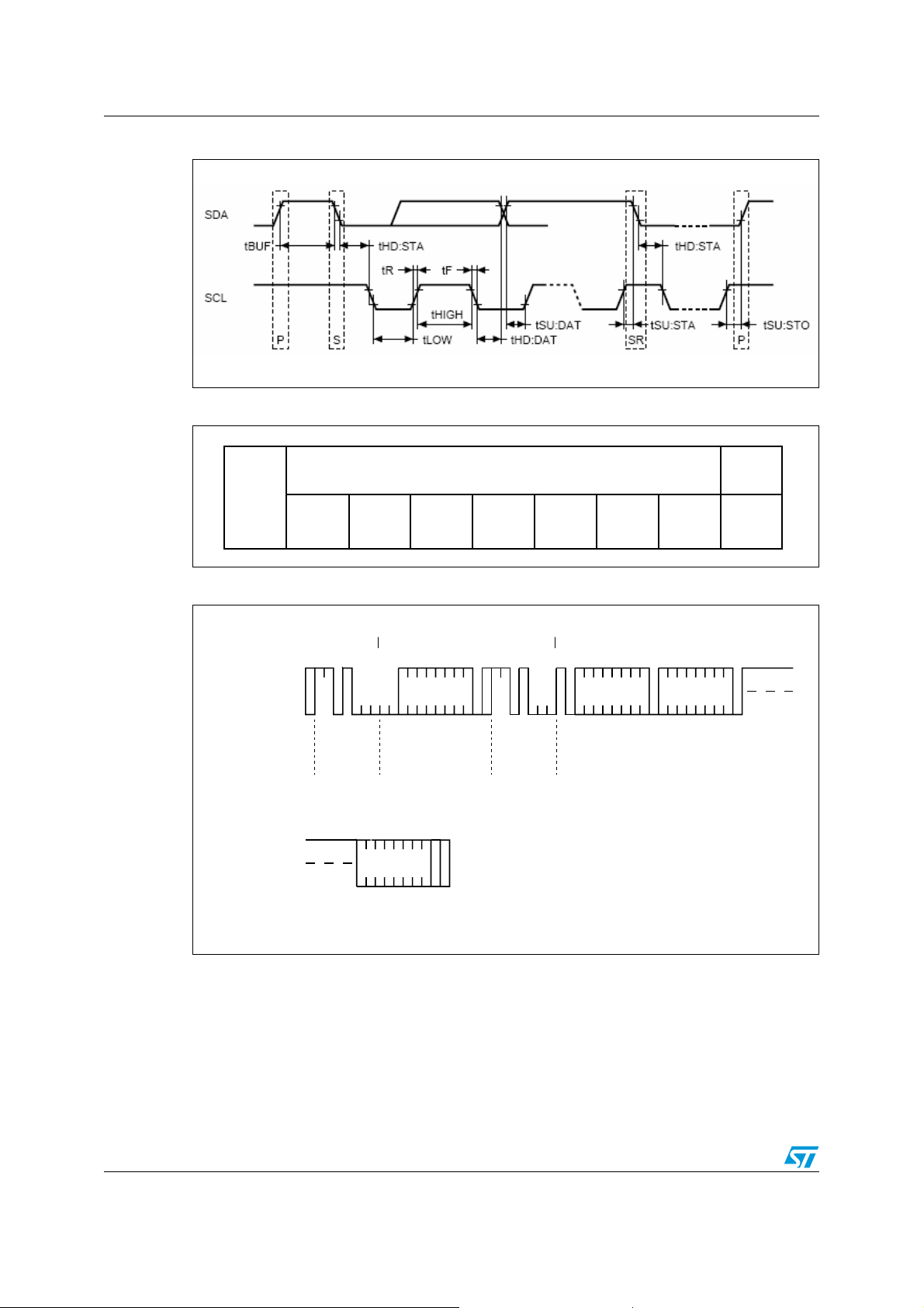
Serial communication format STFPC320
Figure 50. Bus timing requirements sequence
Figure 51. Slave address location
S
S
Figure 52. Read mode sequence
BUS ACTIVITY:
MASTER
SDA LINE
BUS ACTIVITY:
START
S
ADDRESS
SLAVE
R/W
ADDRESS (An)
ACK
DATA n+X
WORD
00
00
STOP
P
Slave Address
Slave Address
START
S
ACK
SLAVE
ADDRESS
R/W
DATA n DATA n+1
ACK
ACK
R/Wbar
R/Wbar
AI00899
1/0
1/0
ACK
10011
10011
NO ACK
66/78
Page 67
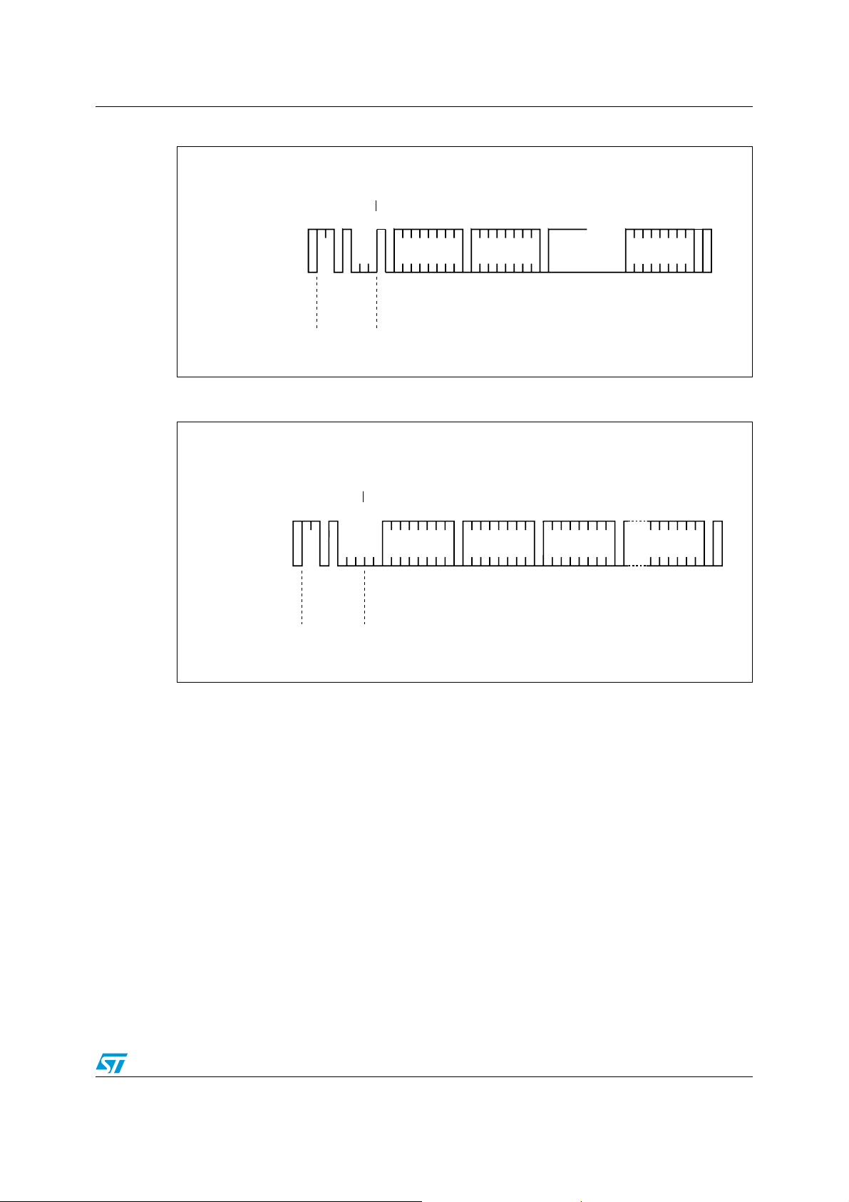
STFPC320 Serial communication format
Figure 53. Alternative READ mode sequence
BUS ACTIVITY:
MASTER
BUS ACTIVITY:
START
S
SLAVE
ADDRESS
R/W
ACK
Figure 54. WRITE mode sequence
BUS ACTIVITY:
MASTER
BUS ACTIVITY:
START
S
ADDRESS
SLAVE
R/W
WORD
ADDRESS (An)
ACK
DATA n DATA n+1 DATA n+X
ACK
DATA n DATA n+1 DATA n+X
ACK
ACK
ACK
ACK
ACK
STOP
PSDA LINE
NO ACK
AI00895
STOP
PSDA LINE
ACK
AI00591
67/78
Page 68

Electrical characteristics STFPC320
17 Electrical characteristics
17.1 Absolute maximum ratings
Table 15. Absolute maximum ratings (TA = 25°C, GND = 0 V)
Symbol Parameter Value Unit
V
DD
V
SS
V
V
O2
I
O1
I
O2
P
T
opt
T
stg
1. Derate at -9.6 mW/°C at TA = 25°C or higher
Logic supply voltage -0.5 to +4.0 V
Driver supply voltage VDD + 0.5 to VDD – 33.3 V
Logic input voltage -0.4 to VDD + 0.5 V
I1
VFP driver output voltage VSS – 0.5 to VDD + 0.5 V
LED driver output current +25 mA
VFP driver output current
Power dissipation 1200
D
Operating ambient temperature -40 to +85 °C
Storage temperature -65 to +150 °C
17.2 Recommended operating conditions
Table 16. Recommended operating conditions (TA = -20 to +70°C, GND = 0V)
Symbol Parameter Min. Typ. Max. Unit
V
DD
V
IH
V
V
SS
Logic supply voltage 3.3 V
High-level input voltage 0.7 V
Low-level input voltage 0 0.3 V
IL
Driver supply voltage 0 VDD - 33.3 V
DD
-40 (grid)
-15 (segment)
(1)
mA
mA
V
DD
DD
V
V
68/78
Page 69

STFPC320 Electrical characteristics
17.3 Power consumption estimation
Maximum power consumption P
= VFD driver dissipation + RL dissipation + LED driver
MAX
dissipation + dynamic power consumption.
Where segment current = 3 mA, grid current = 15 mA and LED current = 20 mA,
FIP driver dissipation = number of segments x 6 + number of grids/(number of grids + 1) x
30 (mW)
R
dissipation = (V
L
– VSS)2/50 x (segment + 1) (mW)
DD
LED driver dissipation = number of LEDs x 20 (mW)
Dynamic power consumption = V
x 5 (mW)
DD
Example:
Where V
= -30 V, VDD = 3.3 V and in 16-segment and 12-digit modes,
SS
FIP driver dissipation = 16 x 6 + 12/13 x 30 = 124
R
dissipation = 33.32/50 x 17 = 377
L
LED driver dissipation = 2 x 20 = 40
Dynamic power consumption = 3.3 x 5 = 16.5
Total = 557.5 mW
69/78
Page 70

Electrical characteristics STFPC320
17.4 Electrical specifications
Table 17. Electrical specifications
(T
= -20 to +70 °C, VDD = 3.3 V, GND = 0 V, VSS = VDD – 33.3 V)
A
Symbol Parameter Test conditions Min Typ Max Unit
V
OH1
V
OL1
V
OL2
I
OH21
I
OH22
I
OLEAK
R
I
I
V
IH
V
IL
V
H
I
DDdyn
High-level output
voltage
Low-level output
voltage
Low-level output
voltage
High-level output
current
High-level output
current
Driver leakage current
Output pull-down
L
resistor
LED1 – LED4,
= -1mA
I
OH1
0.9 V
DD
LED1 – LED4,
I
= 20mA
OH2
SDA, I
= 4mA 0.6 V
OL2
VO = VDD – 2V,
to Seg
Seg
1
= VDD – 2 V, Grid1 to
V
O
12
Grid8, Seg13/Grid16 to
/Grid
Seg
12
9
= VDD – 33.3 V,
V
O
driver off
Driver output 50 100 150 kΩ
Input current VI = VDD or GND ±1 μA
High-level input voltage 0.7 V
DD
Low-level input voltage 0.3 V
Hysteresis voltage 0.35 V
Dynamic current
consumption
Under no load,
display OFF
V
1V
-3 mA
-15 mA
-10 μA
V
DD
V
2mA
R
PU
R
PU
R
PD
External pull-up resistor SCL, SDA 4.7 kΩ
External pull-up resistor IRQ_N/SQW 10 kΩ
External pull-down
resistor
READY, KEY1, KEY2 10 kΩ
70/78
Page 71

STFPC320 Electrical characteristics
17.5 Crystal electrical characteristics
Table 18. Crystal electrical characteristics
Symbol Parameter
(1) (2)
Min Typ Max Units
f
O
R
C
1. Externally supplied. ST recommends the Citizen CFS-145 (1.5x5mm) and the KDS DT-38 (3x8mm) for
thru-hole, or the KDS DMX-26S(3.2x8mm) for surface-mount, tuning fork-type quartz crystals.
KDS can be contacted at kouhou@kdsj.co.jp or http://www.kdsj.co.jp
Citizen can be contacted at csd@citizen-americal.com or http://www.citizencrystal.com
2. Circuit board layout considerations for the 32.768KHz crystal of minimum trace lengths and isolation from
RF generating signals should be taken into account.
3. Guaranteed by design.
Resonant frequency 32.768 kHz
Series resistance 35 40
S
Load capacitance 12.5 pF
L
17.6 Oscillator characteristics
Table 19. Oscillator characteristics
Symbol Parameter Conditions Min Typ Max Unit
V
STA
t
STA
C
C
1. Reference va lue. TA = 25° C, VCC = 3.0V, CFM-145 (CL = 6pF, 32.768 KHz) manufactured by Citizen
Oscillator start voltage ≤10 seconds 1.5 V
Oscillator start time VCC = 3.0 V 1 s
XIN 25 pF
L1
XOUT 25 pF
L2
IC-to-IC frequency
variation
(1)
(3)
kΩ
-10 +10 ppm
71/78
Page 72
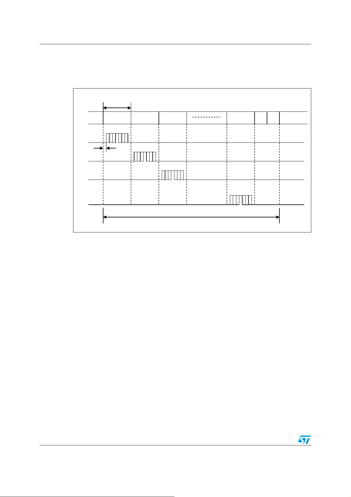
Electrical characteristics STFPC320
17.7 Timing characteristics
VDD = 3.3 V, TA = -20 to 70°C, unless otherwise noted. Typical values are at TA = 25°C
Figure 55. Key scanning and display timing
(1)
≈ 500μs
DIG1 DIG2 DIG3 DIGn
DISP
1 frame = t
DISP
x (n+1)
Key scan data
DIG1
SEG Output
G1
G2
G3
Gn
t
DISP
1/16 t
Note: Pulse width of segment signal is decided by oscillator frequency. The value can be modified
by trimming R
. One cycle of key scann ing consists of one frame and data of 12 x 2
OSC
matrices are stored in RAM.
The keyscan is only at the end of the frame when the display is ON. When the display is
OFF, the key scan takes place continuously. The grid is turned off during the key scan.
72/78
Page 73

STFPC320 Electrical characteristics
17.8 Switching characteristics
Table 20. Switching characteristics
(T
= -20 to +70 °C, VDD = 3.3V, VSS = -30V)
A
Symbol Parameter Min Typ Max Units
f
SCL
t
LOW
t
HIGH
t
R
t
F
t
HD:STA
t
SU:STA
t
SU:DAT
t
HD:DAT
t
SU:STO
t
BUF
t
rec
t
UNMUTE
t
MUTE
SCL clock frequency 0 400 kHz
Clock low period 1.3 μs
Clock high period 600 ns
SDA and SCL rise time 300 ns
SDA and SCL fall time 300 ns
START condition hold time
(After this period the first clock pulse is generated)
START condition setup time
(only relevant for a repeated start condition)
Data setup time
(1)
600 ns
600 ns
100 ns
Data hold time 0 μs
STOP condition setup time 600 ns
Time the bus must be free before a new
transmission can start
1.3 μs
Watchdog output pulse width 96 98 ms
Time delay of turning off MUTE after READY is
set high
Time delay of turning on MUTE before STBY is
set high
10 80 ns
10 80 ns
1. Transmitter must internally provide a hold time to bridge the undefined region (300ns max) of the falling
edge of the SCL.
Table 21. Switching characteristics (TA = -20 to +70 °C, VDD = 3.3V, VSS = -30V)
Symbol Parameter Test conditiong Min. Typ. Max. Unit
t
OSC
t
PLZ
t
PZL
t
TZH1
t
TZH2
t
THZ
C
Oscillation frequency R = 33 kΩ ± 1% 430 500 565 kHz
Propagation delay
time
Rise time
CLK -> SDA
= 15pF, RL = 10kΩ
C
L
C
= 300pF
L
to Seg
Seg
1
12
Grid1 to Grid8,
Seg13/Grid16 to
/Grid
Seg
20
9
Fall time CL = 300pF, Segn, Grid
Input capacitance 15 pF
I
n
73/78
300 ns
100 ns
2 μs
0.5 μs
120 μs
Page 74

STFPC320 typical application circuit STFPC320
18 STFPC320 typical application circuit
C2
C2
1
1
2
2
3
3
4
4
4
4
5
5
6
6
7
7
8
8
9
9
10
10
1
1
12
12
13
13
GND
GND
R3
R3
R4
R4
R
R
PU
PU
VDD 3.3V±10%
VDD 3.3V±10%
VSS
VSS
GND
GND
VDD
VDD
R
R
OSC
OSC
OSC
OSC
PIN_AV8
PIN_AV8
SCL
SCL
SDA
SDA
IR_DATA_IN
IR_DATA_IN
SW1, SW2
SW1, SW2
IRQ_N/SQW
IRQ_N/SQW
MUTE
MUTE
STBY
STBY
R
R
PD
PD
GND
GND
KEY1 KEY2
KEY1 KEY2
READY
READY
D1
D1
SEG1/K1
SEG1/K1
+
+
+
C
C
C
Figure 56. Typical applica tion circuit
VDD
VDD
+
+
C1
C1
<
<
<
<
<
<
<
<
<
<
<
<
<
<
<
<
<
<
<
<
<
<
<
<
<
<
STFPC320
STFPC320
XIN
XIN
C
C
L1
L2
L1
L1
L2
12 x 2
12 x 2
KEYBOARD
KEYBOARD
XOUT
XOUT
VSS
VSS
+
+
D12
D12
SEG12/K12
SEG12/K12
S13/G16 ~ S20/G9
S13/G16 ~ S20/G9
G1 ~ G8
G1 ~ G8
LED1
LED1
LED2
LED2
LED3
LED3
LED4
LED4
GND
GND
C3 C4
C3 C4
+
+
8 Grids/Segments
8 Grids/Segments
8 Grids
8 Grids
R1
R1
R2
R2
R3
R3
R4
R4
VDD
VDD
VFD
VFD
Ef
Ef
R
= 33kΩ (±1%) for oscillator resistor;
OSC
R1 ~ R4 = 0.75 ~ 1.2kΩ;
R3, R4 = 10kΩ for external keyboard pull-down resistor;
= 4.7kΩ for external pull-up resistor on SDA, SCL;
R
PU
= 10kΩ for external pull-up resistor on IRQ_N/SQW;
R
PU
RPD = 10kΩ for external pull-down resistor on READY;
, CL2 = 25pF;
C
L1
C1 = 33µF-25V electrolytic;
74/78
C2 = 0.01 ~ 0.1µF-25V ceramic;
C3 = 0.01 ~ 0.1µF-63V ceramic;
C4 = 33µF-63V electrolytic;
D1 ~ D12 = 1N4148;
Ef = filament voltage according to the VFD specs;
VDD = 3.3V ±10%;
VSS = down to VDD - 33.3V.
Page 75

STFPC320 Package mechanical data
19 Package mechanical data
In order to meet environmental requirements, ST offers these devices in ECOPACK®
packages. These packages have a Lead-free second level interconnect . The category of
second level interconnect is marked on the package and on the inner box label, in
compliance with JEDEC Standard JESD97. The maximum ratings related t o soldering
conditions are also marked on the inner box label. ECOPACK is an ST trademark.
ECOPACK specifications are available at: www.st.com.
Figure 57. PQFP52L package outline
75/78
Page 76

Package mechanical data STFPC320
Table 22. PQFP52 (10 x 10 x 2 mm) mechanical data
Symbol
Min Typ Max
A2.450
A1 0.250
A2 1.800 2.000 2.200
b 0.220 0.400
c 0.110 0.230
D 12.950 13.200 13.450
D1 9.800 10.000 10.200
D2 7.800
E 12.950 13.200 13.450
E1 9.800 10.000 10.200
E2 7.800
e 0.650
L 0.730 0.880 1.030
L1 1.600
k0
° 7°
ddd 0.100
Millimeters
Figure 58. PQFP-52 carrier tape information
76/78
Page 77

STFPC320 Revision history
20 Revision history
Table 23. Document revision history
Date Revision Changes
08-Jan-2006 1 Initial release.
Document reformatted to conform to new ST template.
07-Jul-2008 2
Modified: package mechanical data.
Added: tape specifications.
77/78
Page 78

STFPC320
Please Read Carefully:
Information in this document is provided solely in connection with ST products. STMicroelectronics NV and its subsidiaries (“ST”) reserve the
right to make changes, corrections, modifications or improvements, to this document, and the products and services described herein at any
time, without notice.
All ST products are sold pursuant to ST’s terms and conditions of sale.
Purchasers are solely res ponsibl e fo r the c hoic e, se lecti on an d use o f the S T prod ucts and s ervi ces d escr ibed he rein , and ST as sumes no
liability whatsoever relati ng to the choice, selection or use o f the ST products and services desc ribed herein.
No license, express or implied, by estoppel or otherwise, to any intellectual property rights is granted under this document. If any part of this
document refers to any third pa rty p ro duc ts or se rv ices it sh all n ot be deem ed a lice ns e gr ant by ST fo r t he use of su ch thi r d party products
or services, or any intellectua l property c ontained the rein or consi dered as a warr anty coverin g the use in any manner whats oever of suc h
third party products or servi ces or any intellectual property contained therein.
UNLESS OTHERWISE SET FORTH IN ST’S TERMS AND CONDITIONS OF SALE ST DISCLAIMS ANY EXPRESS OR IMPLIED
WARRANTY WITH RESPECT TO THE USE AND/OR SALE OF ST PRODUCTS INCLUDING WITHOUT LIMITATION IMPLIED
WARRANTIES OF MERCHANTABILITY, FITNESS FOR A PARTICUL AR PURPOS E (AND THEIR EQUIVALE NTS UNDER THE LAWS
OF ANY JURISDICTION), OR INFRINGEMENT OF ANY PATENT, COPYRIGHT OR OTHER INTELLECTUAL PROPERTY RIGHT.
UNLESS EXPRESSLY APPROVED IN WRITING BY AN AUTHORIZED ST REPRESENTATIVE, ST PRODUCTS ARE NOT
RECOMMENDED, AUTHORIZED OR WARRANTED FOR USE IN MILITARY, AIR CRAFT, SPACE, LIFE SAVING, OR LIFE SUSTAINING
APPLICATIONS, NOR IN PRODUCTS OR SYSTEMS WHERE FAILURE OR MALFUNCTION MAY RESULT IN PERSONAL INJ URY,
DEATH, OR SEVERE PROPERTY OR ENVIRONMENTAL DAMAGE. ST PRODUCTS WHICH ARE NOT SPECIFIED AS "AUTOMOTIVE
GRADE" MAY ONLY BE USED IN AUTOMOTIVE APPLICATIONS AT USER’S OWN RISK.
Resale of ST products with provisions different from the statements and/or technical features set forth in this document shall immediately void
any warranty granted by ST fo r the ST pro duct or serv ice describe d herein and shall not cr eate or exten d in any manne r whatsoever , any
liability of ST.
ST and the ST logo are trademarks or registered trademarks of ST in various countries.
Information in this document su persedes and replaces all information previously supplied.
The ST logo is a registered trademark of STMicroelectronics. All other names are the property of their respective owners.
© 2008 STMicroelectronics - All rights reserved
STMicroelectronics group of compan ie s
Australia - Belgium - Brazil - Canada - China - Czech Republic - Finland - France - Germany - Hong Kong - India - Israel - Italy - Japan -
Malaysia - Malta - Morocco - Singapore - Spain - Sweden - Switzerland - United Kingdom - United States of America
www.st.com
78/78
 Loading...