

现货库存、技术资料、百科信息、热点资讯,精彩尽在鼎好!
3
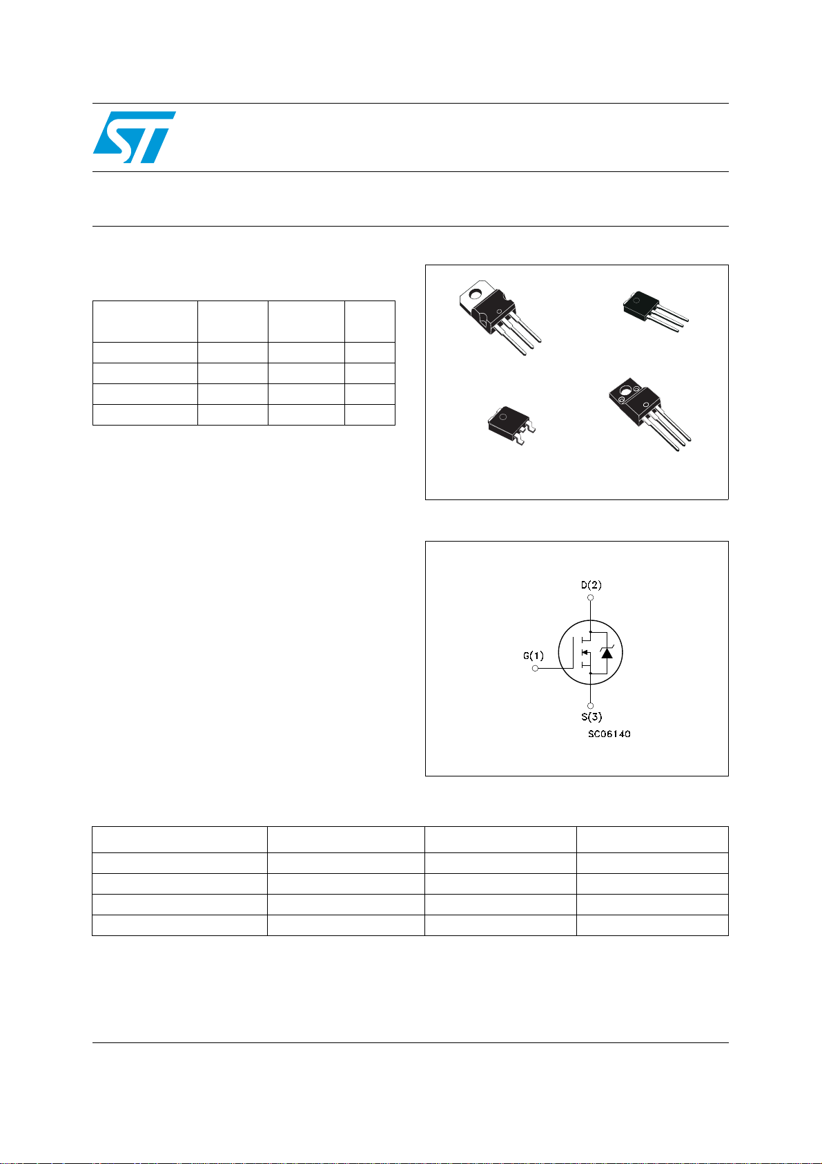
STD7NM50N - STD7NM50N-1
N-channel 500V - 0.70Ω - 5A - TO-220 - TO-220FP - IPAK - DPAK
Second generation MDmesh™ Power MOSFET
Features
V
Type
DSS
(@Tjmax)
STD7NM50N 550V <0.78Ω 5A
STD7NM50N-1 550V <0.78Ω 5A
STF7NM50N 550V <0.78Ω 5A
STP7NM50N 550V <0.78Ω 5A
1. Limited only by maximum temperature allowed
■ 100% avalanche tested
■ Low input capacitance and gate charge
■ Low gate input resistance
Description
R
DS(on)
I
STF7NM50N - STP7NM50N
D
3
(1)
2
1
TO-220
3
1
DPAK
Internal schematic diagram
IPAK
1
TO-220FP
2
1
3
2
This device is realized with the second generation
of MDmesh™ technology. This revolutionary
Power MOSFET associates a new vertical
structure to the company’s strip layout to yield one
of the world’s lowest on-resistance and gate
charge. It is therefore suitable for the most
demanding high efficiency converters
Application
■ Switching application
Order codes
Part number Marking Package Packaging
STD7NM50N-1 D7NM50N IPAK Tube
STD7NM50N D7NM50N DPAK Tape & reel
STF7NM50N F7NM50N TO-220FP Tube
STP7NM50N P7NM50N TO-220 Tube
April 2007 Rev 1 1/17
www.st.com
17

Contents STD7NM50N - STD7NM50N-1 - STF7NM50N - STP7NM50N
Contents
1 Electrical ratings . . . . . . . . . . . . . . . . . . . . . . . . . . . . . . . . . . . . . . . . . . . . 3
2 Electrical characteristics . . . . . . . . . . . . . . . . . . . . . . . . . . . . . . . . . . . . . 4
2.1 Electrical characteristics (curves) . . . . . . . . . . . . . . . . . . . . . . . . . . . . 6
3 Test circuit . . . . . . . . . . . . . . . . . . . . . . . . . . . . . . . . . . . . . . . . . . . . . . . . 9
4 Package mechanical data . . . . . . . . . . . . . . . . . . . . . . . . . . . . . . . . . . . . 10
5 Packaging mechanical data . . . . . . . . . . . . . . . . . . . . . . . . . . . . . . . . . . 15
6 Revision history . . . . . . . . . . . . . . . . . . . . . . . . . . . . . . . . . . . . . . . . . . . 16
2/17
STD7NM50N - STD7NM50N-1 - STF7NM50N - STP7NM50N Electrical ratings
1 Electrical ratings
Table 1. Absolute maximum ratings
Value
Symbol Parameter
TO-220 / DP AK
IPAK
TO-220FP
Unit
V
DS
V
GS
I
I
I
DM
P
TOT
dv/dt
D
D
Drain-source voltage (VGS=0)
Gate-source voltage ± 25 V
Drain current (continuous) at TC = 25°C
Drain current (continuous) at TC = 100°C
(2)
Drain current (pulsed) 20
Total dissipation at TC = 25°C
(3)
Peak diode recovery voltage slope 15 V/ns
Insulation withstand voltage (RMS) from
V
ISO
all three leads to external heat sink
(t=1s;TC=25°C)
T
T
stg
1. Limited only by maximum temperature allowed
2. Pulse width limited by safe operating area
3. ISD ≤ 5A, di/dt ≤ 400A/µs, VDD =80% V
Operating junction temperature
j
Storage temperature
(BR)DSS
Table 2. Thermal data
Symbol Parameter
500 V
5
3
(1)
5
(1)
3
20
45 20 W
-- 2500 V
-55 to 150 °C
Max value
TO-220 / DP AK
IPAK
TO-220FP
(1)
A
A
A
Unit
Rthj-case Thermal resistance junction-case max 2.78 6.25 °C/W
Rthj-amb Thermal resistance junction-amb max 62.5 °C/W
T
Maximum lead temperature for soldering
l
purpose
300 °C
Table 3. Avalanche characteristics
Symbol Parameter Max value Unit
I
AS
E
AS
Avalanche current, repetitive or notrepetitive (pulse width limited by Tj max)
Single pulse avalanche energy
(starting Tj=25°C, I
D=IAS
, VDD= 50V)
2A
100 mJ
3/17
Electrical characteristics STD7NM50N - STD7NM50N-1 - STF7NM50N - STP7NM50N
2 Electrical characteristics
(T
=25°C unless otherwise specified)
CASE
Table 4. On/off states
Symbol Parameter Test conditions Min Typ Max Unit
V
(BR)DSS
dv/dt
I
DSS
I
GSS
V
GS(th)
R
DS(on)
1. Characteristics value at turn off on inductive load
Drain-source breakdown
voltage
(1)
Drain-source voltage slope
Zero gate voltage drain
current (V
GS
= 0)
Gate body leakage current
= 0)
(V
DS
Gate threshold voltage
Static drain-source on
resistance
= 1mA, VGS= 0
I
D
Vdd = 400V, Id = 5A,
Vgs = 10V
V
= Max rating,
DS
V
= Max rating,Tc = 125°C
DS
= ±20V
V
GS
= VGS, ID = 250µA
V
DS
VGS= 10V, ID=2.5A
500 V
40 V/ns
1
100µAµA
100 nA
234V
0.70 0.78 Ω
Table 5. Dynamic
Symbol Parameter Test conditions Min. Typ. Max. Unit
C
oss eq.
(1)
g
fs
C
C
C
Forward transconductance
Input capacitance
iss
Output capacitance
oss
Reverse transfer
rss
capacitance
Equivalent output
(2)
capacitance
V
DS
V
DS
V
GS
f=1MHz Gate DC Bias=0
Rg Gate input resistance
Test signal level=20mV
Open drain
Q
g
Total gate charge
Q
Q
1. Pulsed: pulse duration = 300µs, duty cycle 1.5%
2. C
increases from 0 to 80% V
Gate-source charge
gs
Gate-drain charge
gd
. is defined as a constant equivalent capacitance giving the same charging time as C
oss eq
DSS
V
DD
V
GS
(see Figure 16)
=15V, ID= 2.5A
= 50V, f =1 MHz, V
GS
= 0
4S
400
35
4
pF
pF
pF
= 0V, VDS = 0V to 400V 67 pF
6 Ω
= 400V, ID = 5A
= 10V
12
2
6
when VDS
oss
nC
nC
nC
4/17

STD7NM50N - STD7NM50N-1 - STF7NM50N - STP7NM50N Electrical characteristics
Table 6. Switching times
Symbol Parameter Test conditions Min Typ Max Unit
t
d(on)
t
d(off)
Turn-on delay time
t
Rise time
r
Turn-off delay time
Fall time
t
f
= 250V, ID = 2.5A,
V
DD
= 4.7Ω, VGS = 10V
R
G
(see Figure 15)
40
7
5
ns
ns
ns
9
ns
Table 7. Source drain diode
Symbol Parameter T est conditions Min Typ Max Unit
I
SD
I
SDM
V
SD
t
Q
I
RRM
t
Q
I
RRM
1. Pulse width limited by safe operating area
2. Pulsed: pulse duration = 300µs, duty cycle 1.5%
Source-drain current
(1)
Source-drain current (pulsed)
(2)
Forward on voltage
rr
Reverse recovery time
Reverse recovery charge
rr
Reverse recovery current
rr
Reverse recovery time
Reverse recovery charge
rr
Reverse recovery current
= 5A, V
I
SD
=5A, di/dt =100A/µs,
I
SD
=100V, Tj=25°C
V
DD
GS
= 0
(see Figure 17)
=5A, di/dt =100A/µs,
I
SD
=100V, Tj=150°C
V
DD
(see Figure 17)
250
2
13
330
2
13
5
20
1.3 V
ns
µC
ns
µC
A
A
A
A
5/17

Electrical characteristics STD7NM50N - STD7NM50N-1 - STF7NM50N - STP7NM50N
2.1 Electrical characteristics (curves)
Figure 1. Safe operating area for TO-220 /
DPAK / IPAK
Figure 2. Thermal impedance for TO-220 /
DPAK / IPAK
Figure 3. Safe operating area for TO-220FP Figure 4. Thermal impedance for TO-220FP
Figure 5. Output characteristics Figure 6. Transfer characteristics
6/17
 Loading...