

ST STB25NM60N-1, STF25NM60N, STP25NM60N, STW25NM60N, STB25NM60N User Manual
查询STB25NM60N供应商
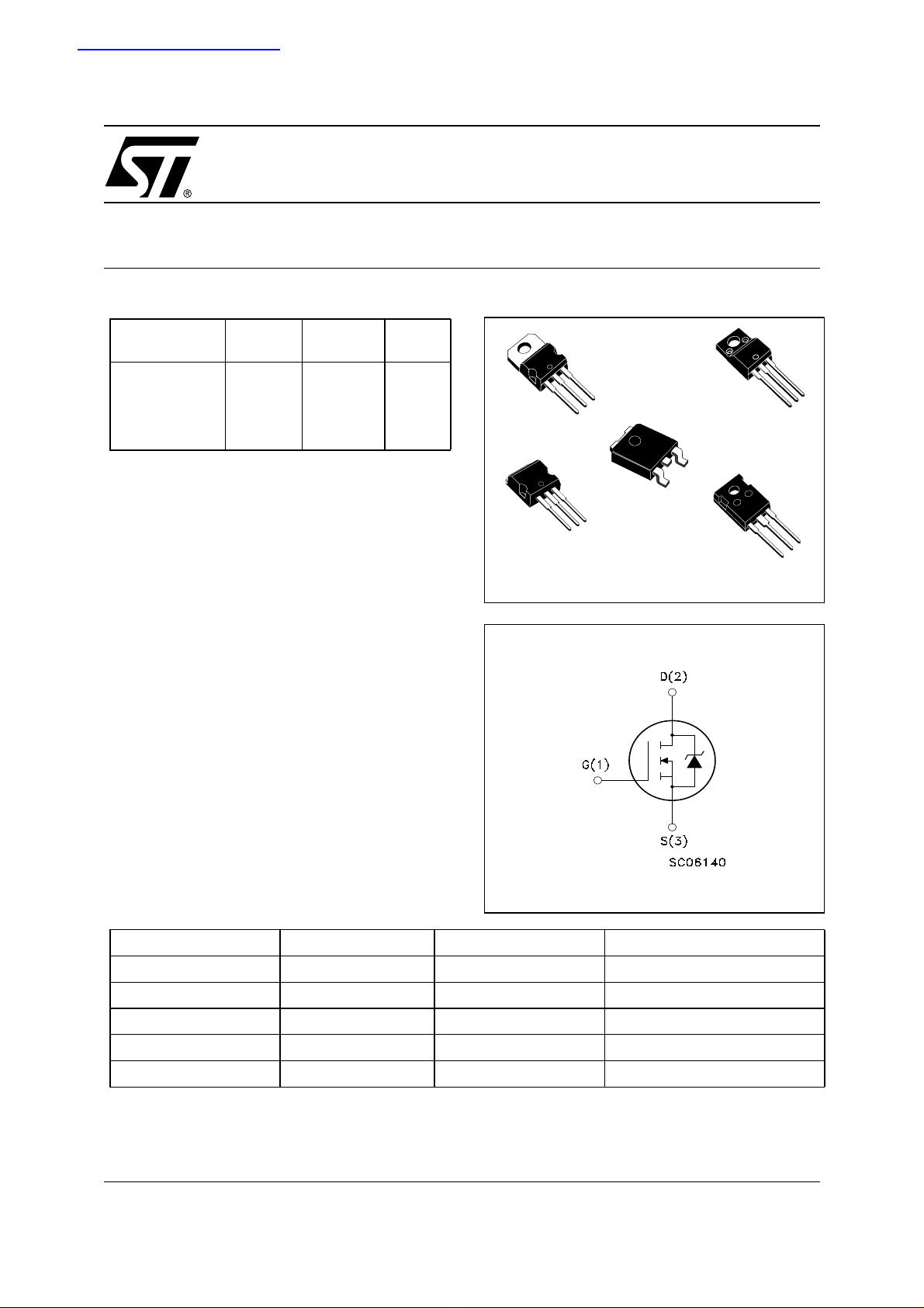
N-CHANNEL 600V 0.140Ω-20A TO-220/FP/D²/I²PAK/TO-247
STP25NM60N - STF25NM60N
STB25N M60N/-1 - STW25NM60N
SECOND GENERATION MDmesh™ MOSFET
PRODUCT PREVIEW
Table 1: Ge neral Features
TYPE V
STB25NM60N-1
STF25NM60N
STP25NM60N
STW25NM60N
STB25NM60N
■ WORLD’S LOWEST ON RESISTANCE
■ TYPICAL R
■ HIGH dv/dt AND AVALANCHE CAPABILITIES
■ 100% AVALANCHE TESTED
■ LOW INPUT CAPACITANCE AND GATE
DS
DSS
(@Tjmax)
650 V
650 V
650 V
650 V
650 V
(on) = 0.140 Ω
R
DS(on)
< 0.170 Ω
< 0.170 Ω
< 0.170 Ω
< 0.170 Ω
< 0.170 Ω
I
D
20 A
20(*) A
20 A
20 A
20 A
CHARGE
■ LOW GATE INPUT RESISTAN CE
DESCRIPTION
The STP25NM60N is realized with the second
generation of MDmesh T echnology. This revolutionary MOSFET associates a new vertical structure to the Company's strip layout to yield the
world's lowest on-resistance and gate charge. It is
therefore suitable for the most demanding high efficiency converters
Figure 1: Package
3
2
TO-220
1
TO-220FP
3
1
D²PAK
3
2
1
I²PAK
TO-247
Figure 2: Internal Schematic Diagram
3
2
1
3
2
1
APPLICATIONS
The MDmesh™ II family is very suitable for increase the power density of high voltage converters allowing system miniaturization and higher
efficiencies.
Table 2: Order Code
SALES TYPE MARKING PACKAGE PACKAGING
STB25NM60N-1 B25NM60N I²PAK TUBE
STF25NM60N F25NM60N TO-220FP TUBE
STP25NM60N P25NM60N TO-220 TUBE
STW25NM60N W25NM60N TO-247 TUBE
STB25NM60N B25NM60N D²PAK TAPE & REEL
June 2005
This is prel i m i nary informat i on on a new product now in dev el opment. Details are sub j ect to change w ithout notic e.
Rev. 4
1/12
STP25NM60N - STF25NM60N - STB25NM 60N/-1 - STW25NM60N
Table 3: Absolute Maximum ratings
Symbol Parameter Value Unit
TO-220/I²PAK
TO-247/D²PAK
Drain-source Voltage (VGS = 0) 600 V
Drain-gate Voltage (RGS = 20 kΩ)600V
Gate- source Voltage ± 25 V
Drain Current (continuous) at TC = 25°C
Drain Current (continuous) at TC = 100°C
20 20 (*) A
12.8 12.8 (*) A
Drain Current (pulsed) 80 80 (*) A
Total Dissipation at TC = 25°C
160 40 W
V
I
DM
V
V
P
DS
DGR
GS
I
D
I
D
(1)
TOT
Derating Factor 1.28 0.32 W/°C
dv/dt (2) Peak Diode Recovery voltage slope TBD V/ns
T
stg
T
j
(*) Limited only by maximum temperature allowed
(1) Pulse wi dt h l i m i ted by safe operating area
≤ 20 A, di/dt ≤ 400 A/µ s, VDD =80%V
(2) I
SD
Storage Temperature – 55 to 150 °C
Max. Operating Junction Temperature 150 °C
.
(BR)DSS
Table 4: Thermal Data
TO-220/I²PAK
TO-247/D²PAK
Rthj-case Thermal Resistance Junction-case Max 0.78 3.1 °C/W
Rthj-amb Thermal Resistance Junction-ambient Max 62.5 °C/W
T
l
Maximum Lead Temperature For Soldering Purpose 300 °C
TO-220FP
TO-220FP
Table 5: Avalanche Characteristics
Symbol Parameter Max Value Unit
I
AS
E
AS
Avalanche Current, Repetitive or Not-Repetitive
(pulse width limited by T
max)
j
Single Pulse Avalanche Energy
(starting T
= 25 °C, ID = IAS, VDD = 50 V)
j
ELECTRICAL CHARACTERISTICS (T
=25°C UNLESS OTHERWISE SPECIFIED)
CASE
TBD A
TBD mJ
Table 6: On /Off
Symbol Parameter Test Conditions Value Unit
Min. Typ. Max.
V
(BR)DSS
Drain-source Breakdown
Voltage
dv/dt(2) Drain Source Voltage
Slope
I
DSS
I
GSS
V
GS(th)
R
DS(on
Zero Gate Voltage
Drain Current (V
GS
= 0)
Gate-body Leakage
Current (V
DS
= 0)
Gate Threshold Voltage
Static Drain-source On
Resistance
(2) Characteristic value at turn off on inductive load
ID = 1 mA, VGS = 0 600 V
Vdd=TBD, Id=TBD, Vgs=TBD TBD V/ns
V
= Max Rating
DS
V
= Max Rating, TC = 125°C
DS
V
= ± 20 V 100 nA
GS
V
= VGS, ID = 250 µA 2
DS
3
1
10
4V
VGS = 10 V, ID = 10 A 0.140 0.170 Ω
µA
µA
2/12
STP25NM60N - STF25NM60N - STB25NM 60N/-1 - STW25NM60N
ELECTRICAL CHARACTERISTICS (CONTINUED)
Table 7: Dynamic
Symbol Parameter Test Conditions Min. Typ. Max. Unit
(1) Forward Transconductance VDS = 15V , ID= 10A 17 S
g
fs
C
iss
C
oss
C
rss
C
OSS eq
R
G
t
d(on)
t
r
t
d(off)
t
f
Q
g
Q
gs
Q
gd
Table 8: Source Drain Diode
Symbol Parameter Test Conditions Min. Typ. Max. Unit
I
SD
I
SDM
VSD (1)
t
rr
Q
rr
I
RRM
t
rr
Q
rr
I
RRM
(1) Pulsed: Pulse duration = 300 µs, duty cycl e 1.5 %.
(2) Pulse width limited by safe operating area.
(3) C
oss eq.
Input Capacitance
Output Capacitance
= 25 V, f = 1 MHz,
V
DS
VGS = 0
Reverse Transfer
Capacitance
(3).Equivalent Outpu t
VGS = 0 V, VDS = 0 to 480 V TBD pF
Capacitance
Gate Input Resistance f=1 MHz Gate DC Bias = 0
Test Signal Level = 20mV
Open Drain
Turn-on Delay Time
Rise Time
Turn-off-Delay Time
= 300 V, ID = 10 A,
V
DD
R
= 4.7 Ω, V
G
(see Figure 4)
GS
= 10 V
Fall Time
= 480 V, ID = 20 A,
Total Gate Charge
Gate-Source Charge
Gate-Drain Charge
V
DD
V
= 10 V
GS
(see Figure 7)
Source-drain Current
(2)
Source-drain Current (pulsed)
Forward On Voltage
Reverse Recovery Time
Reverse Recovery Charge
Reverse Recovery Current
Reverse Recovery Time
Reverse Recovery Charge
Reverse Recovery Current
is defined as a constant equivalent capacitance giving the same charging time as C
ISD = 20 A, VGS = 0
= 25 A, di/dt = 100 A/µs
I
SD
VDD = 100V
(see Figure 5)
= 25 A, di/dt = 100 A/µs
I
SD
VDD = 100V, Tj = 150°C
(see Figure 5)
2565
511
77
2 Ω
TBD
TBD
TBD
TBD
93
TBD
TBD
20
80
1.3 V
TBD
TBD
TBD
TBD
TBD
TBD
when VDS increase s from 0 to 80% V
oss
pF
pF
pF
ns
ns
ns
ns
nC
nC
nC
ns
µC
ns
µC
A
A
A
A
DSS
.
3/12
STP25NM60N - STF25NM60N - STB25NM 60N/-1 - STW25NM60N
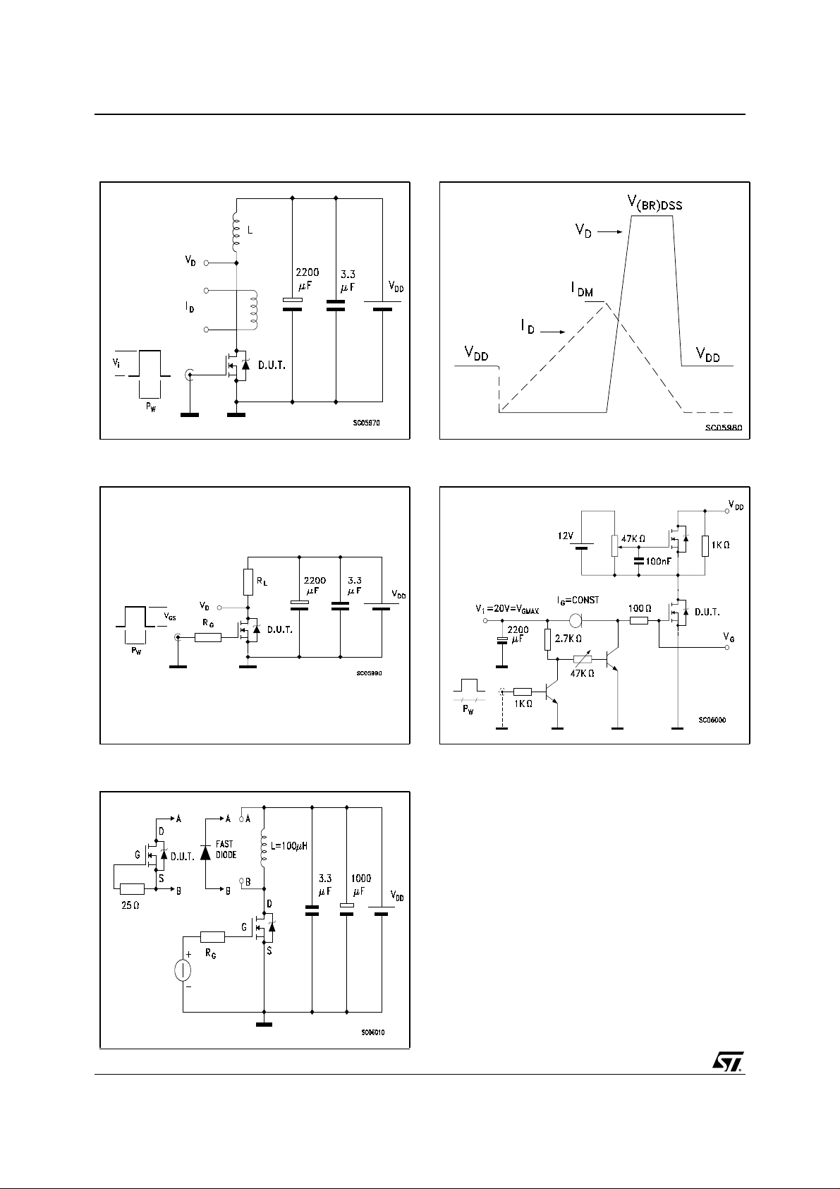
Figure 3: Unclamped Inductive Load Test Circuit
Figure 4: Switching Times Test Circuit For Resistive Load
Figure 6: Unclamped Inductive Wafeform
Figure 7: Gate Charge Test Circuit
Figure 5: Test Circuit For Inductive Load
Switching and Diode Recovery Times
4/12
 Loading...