

1
3
1
3
3
3
1
3
查询STB21NM50N供应商
STP21NM50N-STF21NM50N-STW21NM50N
STB21NM50N - STB21NM50N-1
N-CH A NNEL 500V - 0.15Ω - 18A TO-220/FP/D2/I2PAK/TO-247
SECOND GENERATION MDmesh™ MOSFET
Table 1: General Features
TYPE V
STB21NM50N
STB21NM50N-1
STF21NM50N
STP21NM50N
STW21NM50N
■ 100% AVALANCHE TESTED
■ LOW INPUT CAPACITANCE AND GATE
DSS
(@Tjmax)
550 V
550 V
550 V
550 V
550 V
R
DS(on)
< 0.19 Ω
< 0.19 Ω
< 0.19 Ω
< 0.19 Ω
< 0.19 Ω
I
D
18 A
18 A
18 A (*)
18 A
18 A
CHARGE
■ LOW GATE INPUT RESISTANCE
DESCRIPTION
The STx21NM50N is realized with the second
generation of MDmesh Techno logy. This revolu
tionary MOSFET associates a new vertical structure to the Comp any's strip layout to yield one of
the world's lowest on-resistance and gate charge.
It is therefore suitable for the most demanding high
efficiency converters
APPLICATIONS
The MDmesh™ II family is very suitable for increasing power density of high voltage converters
allowing system miniaturization and higher effi
ciencies.
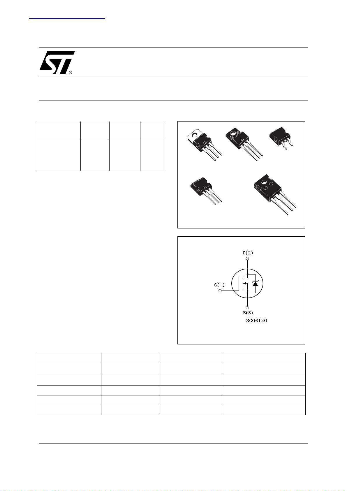
Figure 1: Package
2
TO-247
TO-220
I2PAK
1
2
TO-220FP
2
Figure 2: Internal Schematic Diagram
D
2
PAK
1
2
Table 2: Order Codes
SALES TYPE MARKING PACKAGE PACKAGING
STB21NM50N B21NM50N
STB21NM50N-1 B21NM50N
STF21NM50N F21NM50N TO-220FP TUBE
STP21NM50N P21NM50N TO-220 TUBE
STW21NM50N W21NM50N TO-247 TUBE
D2PAK
I2PAK
TAPE & REEL
TUBE
Rev. 3
1/16October 2005
STP21NM50N - STF21NM50N - STB21NM 50N - STB21NM50N-1 - STW21NM50N
Table 3: Absolute Maximum ratings
Symbol Parameter Value Unit
TO-220 / D2PAK / I2PAK
/ TO-247
V
DS
V
DGR
V
GS
I
D
I
D
IDM ()
P
TOT
Drain-source Voltage (VGS = 0) 500 V
Drain-gate Voltage (RGS = 20 kΩ) 500 V
Gate- source Voltage ±25 V
Drain Current (continuous) at TC = 25°C
Drain Current (continuous) at TC = 100°C
18 18 (*) A
11 11 (*) A
Drain Current (pulsed) 72 72 (*) A
Total Dissipation at TC = 25°C
140 30 W
Derating Factor 1.12 0.23 W/°C
dv/dt(1) Peak Diode Recovery voltage slope 15 V/ns
Viso Insulation Winthstand Voltage (DC) -- 2500 V
T
stg
T
Storage Temperature
Max. Operating Junction Temperature
j
–55 to 150
150
() Pulse width l i mited by safe operating area
(*) Limited only by maximum temperature allowed
(1) ISD ≤ 18 A, di/dt ≤ 40 0 A / µs, VDD =80% V
(BR)DSS
TO-220FP
°C
Table 4: Thermal Data
TO-220 / D²PAK / I²PAK
/ TO-247
Rthj-case Thermal Resistance Junction-case Max 0.89 4.21 °C/W
Rthj-amb Thermal Resistance Junction-ambient Max 62.5 °C/W
T
Table 5: Avalanche Characteristics
Maximum Lead T emperature For Soldering
l
Purpose
300 °C
Symbol Parameter Max Value Unit
I
AS
Avalanche Current, Repetitive or Not-Repetitive
(pulse width limited by Tj max)
E
AS
Single Pulse Avalanche Energy
(starting Tj = 25 °C, ID = IAR, VDD = 50 V)
TO-220FP
9 A
480 mJ
2/16
STP21NM50N - STF21NM50N - ST B21NM50N - STB21NM50N-1 - STW21NM50N
ELECTRICAL CHARACTERISTICS (T
=25°C UNLESS OTHERWISE SPECIFIED)
CASE
Table 6: On/Off
Symbol Parameter Test Conditions Value Unit
Min. Typ. Max.
V
(BR)DSS
Drain-source
ID = 1mA, VGS = 0 500 V
Breakdown Voltage
dv/dt(2) Drain Source Voltage
Vdd=400V, Id=25A, Vgs=10V 44 V/ns
Slope
I
DSS
Zero Gate Voltage
Drain Current (VGS = 0)
VDS = Max Rating
VDS = Max Rating
1
10
TC = 125 °C
I
GSS
Gate-body Leaka ge
VGS = ± 20V 100 nA
Current (VDS = 0)
V
GS(th)
R
DS(on)
Gate Threshold Voltage VDS = VGS, ID = 250 µA 2 3 4 V
Static Drain-source On
VGS = 10V, ID = 9 A 0.150 0.190 Ω
Resistance
(2) Cha rac teristic va l ue at turn off on inductive loa d
Table 7: Dynamic
Symbol Parameter Test Conditions Min. Typ. Max. Unit
g
(1) Forward Transconductance VDS = 15 V, ID = 9 A
fs
C
oss eq.
C
iss
C
oss
C
rss
Input Capacitance
Output Capacitance
Reverse Transfer
Capacitance
(*) E quiv alent Outpu t
VDS = 25V, f = 1 MHz, VGS = 0 1950
VGS = 0V, VDS = 0V to 400V 270 pF
Capacitance
t
d(on)
t
d(off)
Q
Q
Q
R
t
r
t
f
g
gs
gd
g
Turn-on Delay Time
Rise Time
Off-voltageRise Time
VDD =250 V, ID = 9 A
RG = 4.7Ω VGS = 10 V
(see Figure 18)
Fall Time
Total Gate Charge
Gate-Source Charge
Gate-Drain Charge
VDD = 400V, ID = 18 A,
VGS = 10V,
(see Figure 21)
Gate Input Resistance f=1MHz Gate DC Bias=0
Test Signal Level=20mV
Open Drain
(*) C
is defined as a co nstant equi valent capaci tance giving the same charging time as C
oss eq.
when VDS increases from 0 to 80% V
oss
12 S
420
60
22
18
90
30
65
10
30
1.6 Ω
µA
µA
pF
pF
pF
ns
ns
ns
ns
nC
nC
nC
DSS
Table 8: Source Drain Diode
Symbol Parameter Test Conditions Min. Typ. Max. Unit
I
SD
I
SDM
VSD (1)
t
rr
Q
rr
I
RRM
t
rr
Q
rr
I
RRM
Note: 1. Puls ed: Pulse du rat i on = 300 µs, d uty cycle 1.5 % .
Source-drain Current
Source-drain Current (pulsed)
Forward On Voltage
Reverse Recovery Time
Reverse Recovery Charge
Reverse Recovery Current
Reverse Recovery Time
Reverse Recovery Charge
Reverse Recovery Current
ISD = 18 A, VGS = 0
ISD = 18 A, di/dt = 100 A/µs
VDD = 100 V, Tj = 25°C
(see Figure 19)
ISD = 18A, di/dt = 100 A/µs
VDD = 100 V, Tj = 150°C
(see Figure 19)
360
5
27
640
6.5
27
18
72
1.5 V
A
A
ns
µC
A
ns
µC
A
3/16
STP21NM50N - STF21NM50N - STB21NM 50N - STB21NM50N-1 - STW21NM50N
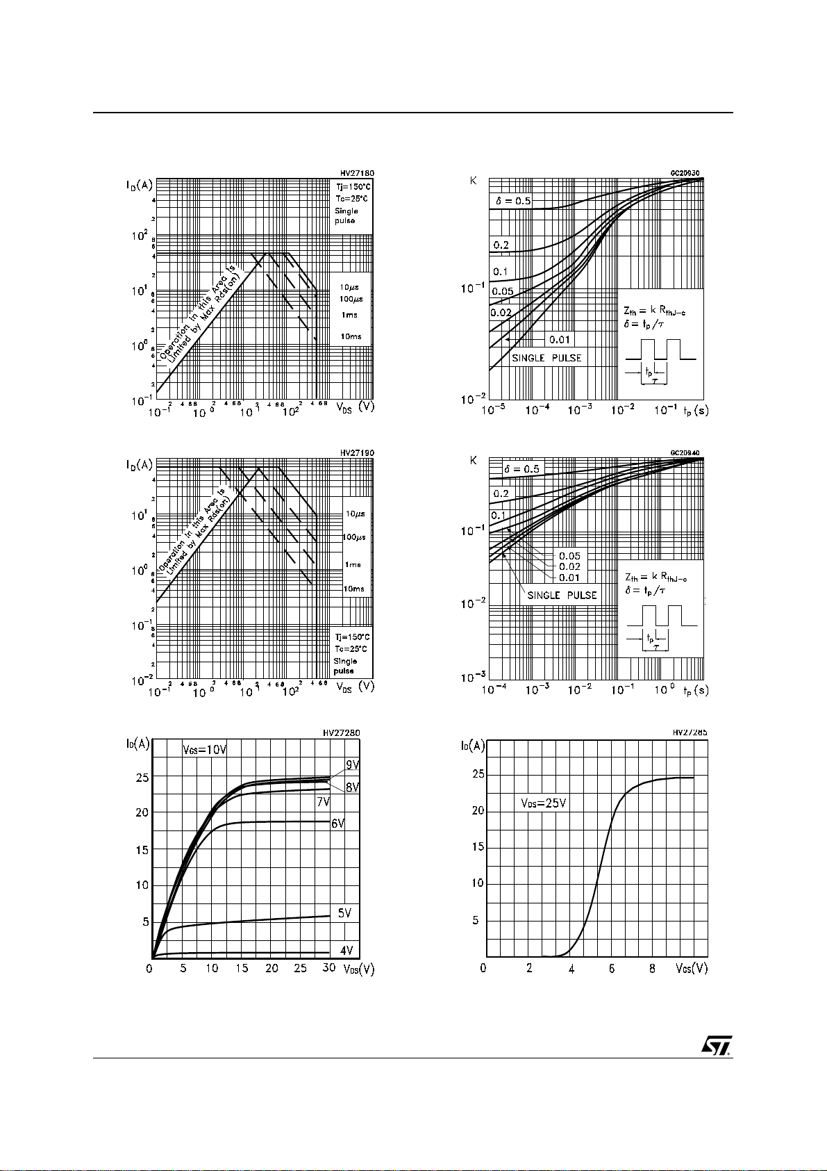
Figure 3: Safe Operating Area For TO-220
Figure 4: Safe Operating Area For TO-220FP
Figure 6: Thermal Impedance For TO-220
Figure 7: Thermal Impedance For TO-220FP
Figure 5: Output Characteristics
4/16
Figure 8: Transfer Characteristics
STP21NM50N - STF21NM50N - ST B21NM50N - STB21NM50N-1 - STW21NM50N
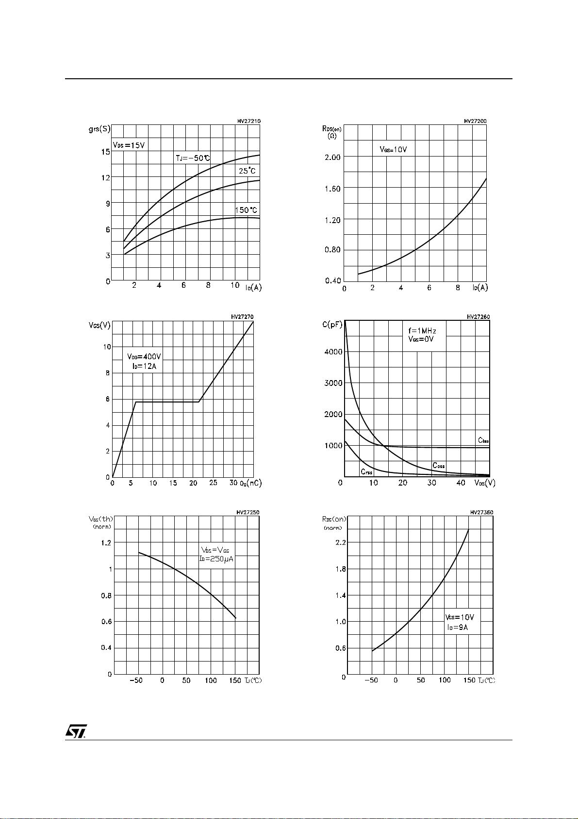
Figure 9: Transconductance
Figure 10: Gate Charge vs Gate-source Voltage
Figure 12: Static Drain-source On Resistance
Figure 13: Capacitance Variations
Figure 11: Normalized Gate Threshold Voltage
vs Tem pera tur e
Figure 14: Normal ized On R esistance vs Temperature
5/16
 Loading...