

STP11NM80 - STF11NM80
STB11NM80 - STW11NM80
N-CHANNEL 800V - 0.35 Ω - 11 A TO-220 /FP/D2PAK/TO-247
MDmesh™ MOSFET
Tabl e 1 : General Feat ures
TYPE V
STP11NM80
STF11NM80
STB11NM80
STW11NM80
■ TYPICA L R
■ LOW GATE INPUT RESISTANCE
■ LOW INPUT CAPACITANCE AND GATE
DSSRDS(on)RDS(on)*QgID
800 V
800 V
800 V
800 V
DS
< 0.40 Ω
< 0.40 Ω
< 0.40 Ω
< 0.40 Ω
(on) = 0.35 Ω
14 Ω∗nC
14 Ω∗nC
14 Ω∗nC
14 Ω∗nC
11 A
11 A
11 A
11 A
CHARGE
■ BEST R
(on)*Qg IN THE INDUSTRY
DS
DESCRIPTION
The MDmesh™ associates the Multiple Drain process with the Company’s PowerMesh™ horizontal
layout assuring an oustanding low on-resistance.
The adoption of the Company’s proprietary strip
technique yields overall dynamic performance that
is significantly better than that of similar compe tition’s products.
APPLICATIONS
The 800 V MDmes h™ family is very suitable for
single swit ch a pplicat ion s in part icula r for Fl yba ck
and Forward converter topologies and for ignition
circuits in the field of lighting.
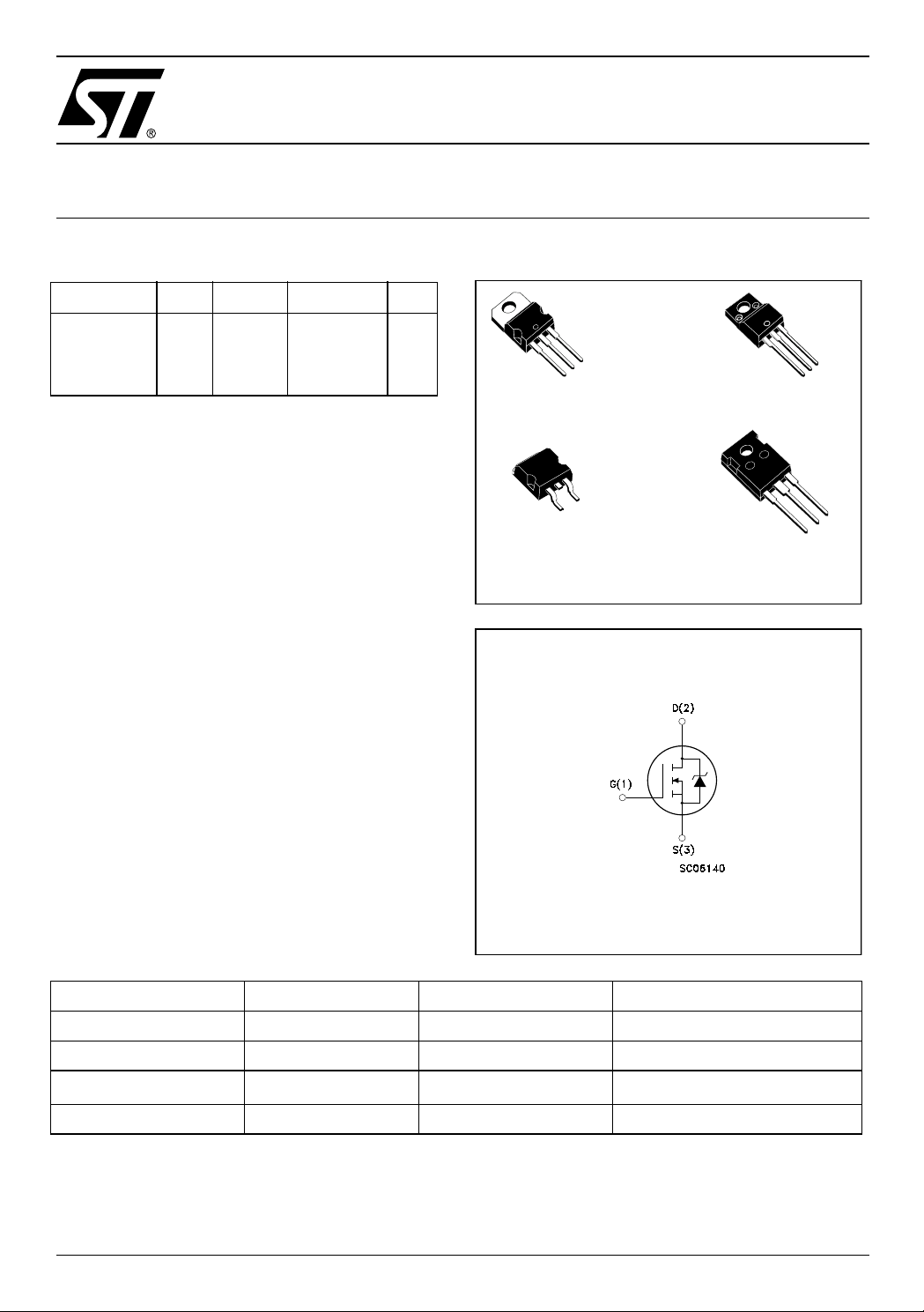
Figure 1: Package
3
2
1
TO-220
2
PAK
D
3
1
TO-220FP
TO-247
Figure 2: Internal Schematic Diagram
3
2
1
3
2
1
Table 2: Order Codes
SALES TYPE MARKING PACKAGE PACKAGING
STP11NM80 P11NM80 TO-220 TUBE
STF11NM80 F11NM80 TO-220FP TUBE
STB11NM80T4
STW11NM80 W11NM80 TO-247 TUBE
B11NM80
2
D
PAK
TAPE & REEL
Rev. 2
1/14September 2004
STP11NM8O - STF11NM80 - STB11N M 80 - STW11NM80
Table 3: Absolute Maximum ratings
Symbol Parameter Value Unit
2
TO-220/D
V
I
DM
P
V
DGR
V
I
I
TOT
DS
GS
D
D
Drain-source Voltage (VGS = 0)
Drain-gate Voltage (RGS = 20 kΩ)
Gate- source Voltage ± 30 V
Drain Current (continuous) at TC = 25°C
Drain Current (continuous) at TC = 100°C
()
Drain Current (pulsed) 44
Total Dissipation at TC = 25°C
Derating Factor 1.2 0.28 W /°C
T
j
T
stg
(
) Pulse width l i m i t ed by safe oper at i ng area
(*) Limit ed only by the Maximum Te mperature All owed
Operating Junction Temperature
Storage Temperature
Table 4: Thermal Data
TO-220/D
TO-247
Rthj-case Thermal Resistance Junction-case Max 0.83 3.6 °C/W
Rthj-amb Thermal Resistance Junction-ambient Max 62.5 °C/W
T
l
Maximum Lead Temperature For Soldering
Purpose
PAK
TO-247
TO-220FP
800 V
800 V
11
4.7
11 (*)
4.7 (*)
44 (*)
150
35
-65 to 150 °C
2
PAK
TO-220FP Unit
300 °C
A
A
A
W
Table 5: Avalanche Characteristics
Symbol Parameter Max Value Unit
I
AR
E
AS
Avalanche Current, Repetitive or Not-Repetitive
(pulse width limited by T
max)
j
Single Pulse Avalanche Energy
(starting T
= 25 °C, ID = 2.5A, VDD = 50 V)
j
2.5 A
400 mJ
2/14

STP11NM8O - STF11NM80 - STB11NM80 - STW11NM80
ELECTRICAL CHARACTERISTICS (T
=25°C UNLESS OTHERWISE SPECIFIED)
CASE
Table 6: On/Off
Symbol Parameter Test Conditions Min. Typ. Max. Unit
V
(BR)DSS
Drain-source
ID = 250 µA, VGS = 0 800 V
Breakdown Voltage
I
DSS
I
GSS
V
GS(th)
R
DS(on)
Zero Gate Voltage
Drain Current (V
GS
= 0)
Gate-body Leaka ge
Current (V
DS
= 0)
Gate Threshold Voltage
Static Drain-source On
V
= Max Rating
DS
V
= Max Rating, TC = 125 °C
DS
V
= ± 30V 100 nA
GS
V
= VGS, ID = 250 µA
DS
345V
10
100
VGS = 10V, ID =5.5 A 0.35 0.40 Ω
Resistance
Table 7: Dynamic
Symbol Parameter Test Conditions Min. Typ. Max. Unit
g
(1) Forward Transconductance VDS > I
fs
C
C
C
R
t
d(on)
t
d(off)
Q
Q
Q
iss
oss
rss
t
r
t
f
gs
gd
G
g
Input Capacitance
Output Capacitance
Reverse Transfer
Capacitance
Gate Input Resistance f=1 MHz Gate DC Bias = 0
Turn-on Delay Time
Rise Time
Turn-off Delay Time
Fall Time
Total Gate Charge
Gate-Source Charge
Gate-Drain Charge
ID = 7.5 A
V
DS
Test Signal Level = 20mV
Open Drain
V
DD
RG=4.7Ω VGS = 10 V
(Resistive Load see, Figure 4)
V
DD
VGS = 10V
D(on)
x R
DS(on)max,
8S
= 25 V, f = 1 MHz, VGS = 0 1630
750
30
2.7 Ω
= 400 V, ID = 5.5 A
22
17
46
15
= 640 V, ID = 11 A,
43.6
11.6
21
µA
µA
pF
pF
pF
ns
ns
ns
ns
nC
nC
nC
Table 8: Source Drain Diode
Symbol Parameter Test Conditions Min. Typ. Max. Unit
I
SD
I
(2)
SDM
(1)
V
SD
t
rr
Q
rr
I
RRM
t
rr
Q
rr
I
RRM
Note: 1. Pulsed: P ul se duration = 300 µs, duty cycle 1.5 % .
2. Pulse wi dt h l i m ited by safe op erating area.
Source-drain Current
Source-drain Current (pulsed)
Forward On Voltage
Reverse Recovery Time
Reverse Recovery Charge
Reverse Recovery Current
Reverse Recovery Time
Reverse Recovery Charge
Reverse Recovery Current
ISD = 11 A, VGS = 0
I
SD
V
DD
(see test circuit, Figure 5)
I
SD
V
DD
(see test circuit, Figure 5)
= 11 A, di/dt = 100 A/µs
= 50 V, Tj = 25°C
= 11 A, di/dt = 100 A/µs
= 50 V, Tj = 150°C
612
7.22
23.6
970
11.25
23.2
11
44
0.86 V
A
A
ns
µC
A
ns
µC
A
3/14
STP11NM8O - STF11NM80 - STB11N M 80 - STW11NM80
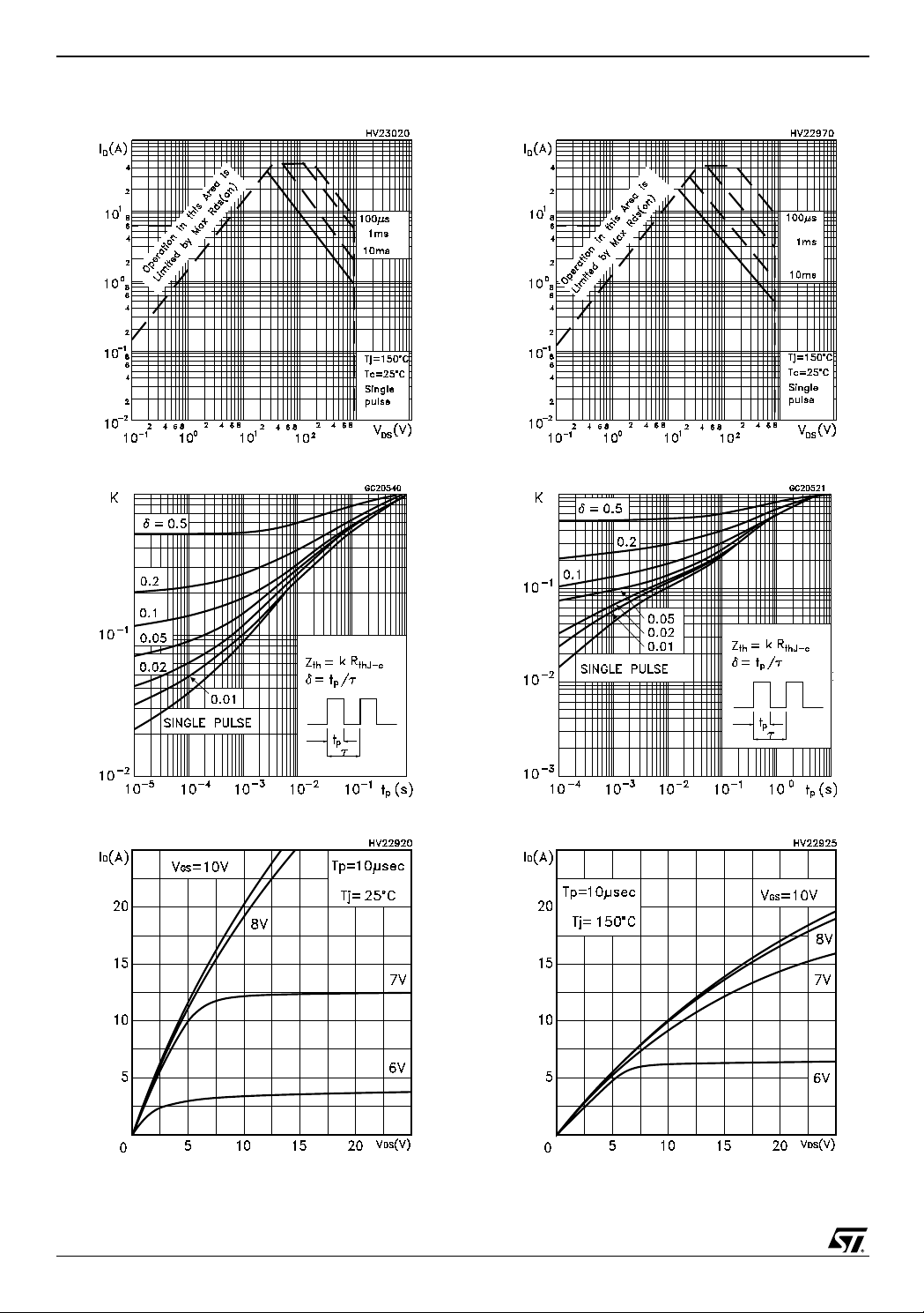
Figure 3: Safe Operating Area For D2PAK/ TO-247 / TO-220
Figure 4: Thermal Impedance For D
2
PAK/
TO-247 / TO-220
Figure 6: Safe Operating Area For TO-220FP
Figure 7: Thermal Impedance For TO-220FP
Figure 5: Output Characteristics
4/14
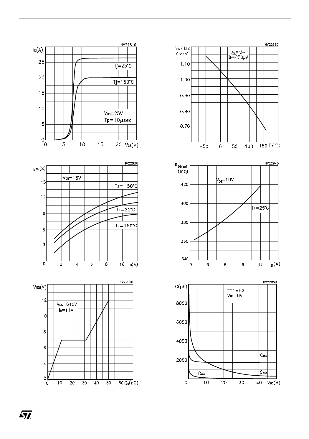
Figure 8: Output Characteristics
STP11NM8O - STF11NM80 - STB11NM80 - STW11NM80
Figure 9: Transfer Characteristics
Figure 10: Transconductance
Figure 12: Normalized Gate Threshold Voltage vs Tem perature
Figure 13: Static Drain-Source On Resistance
Figure 11: Gate Charge vs Gate-source Voltage
Figure 14: Capacitance Variations
5/14
 Loading...