

ST STE70NM60 User Manual

查询STE70NM60供应商
STE70NM60
N-CHANNEL 600V - 0.050Ω - 70A ISOTOP
Zener-Protected MDmesh™Power MOSFET
TYPE V
STE70NM60 600V < 0.055Ω 70 A
TYPICAL RDS(on) = 0.050Ω
HIGH dv/dt AND AVALANCHE CAPABILITIES
IMPROVED ESD CAPABILITY
LOW INPUT CAPACITANCE AND GATE
DSS
R
DS(on)
I
D
CHARGE
LOW GATE INPUT RESISTANCE
TIGHT PROCESS CONTROL
INDUSTRY’S LOWEST ON-RESISTANCE
DESCRIPTION
The MDmes h™ is a new revolutionary MOSFET
technology that associates the Multiple Drain process with the Company’s PowerMESH™ horizontal
layout. Theresulting produc t has an outstanding low
on-resistance, impressively high dv/dt and excellent
avalanche characteristics. The adoption of the
Company’s proprietary strip technique yields overall
dynamic perfo rmance that issignificantly better than
that of similar competition’s products.
APPLICATIONS
The MDmesh™ family is very suitable for increas ing
power densi ty of high voltage converters allowing
system miniaturization and higher efficiencies.
ISOTOP
INTERNAL SCHEMATIC DIAGRAM
ORDERING INFORMATION
SALES TYPE MARKING PACKAGE PACKAGING
STE70NM60 E70NM60 ISOTOP TUBE
1/8March 2003
STE70NM60
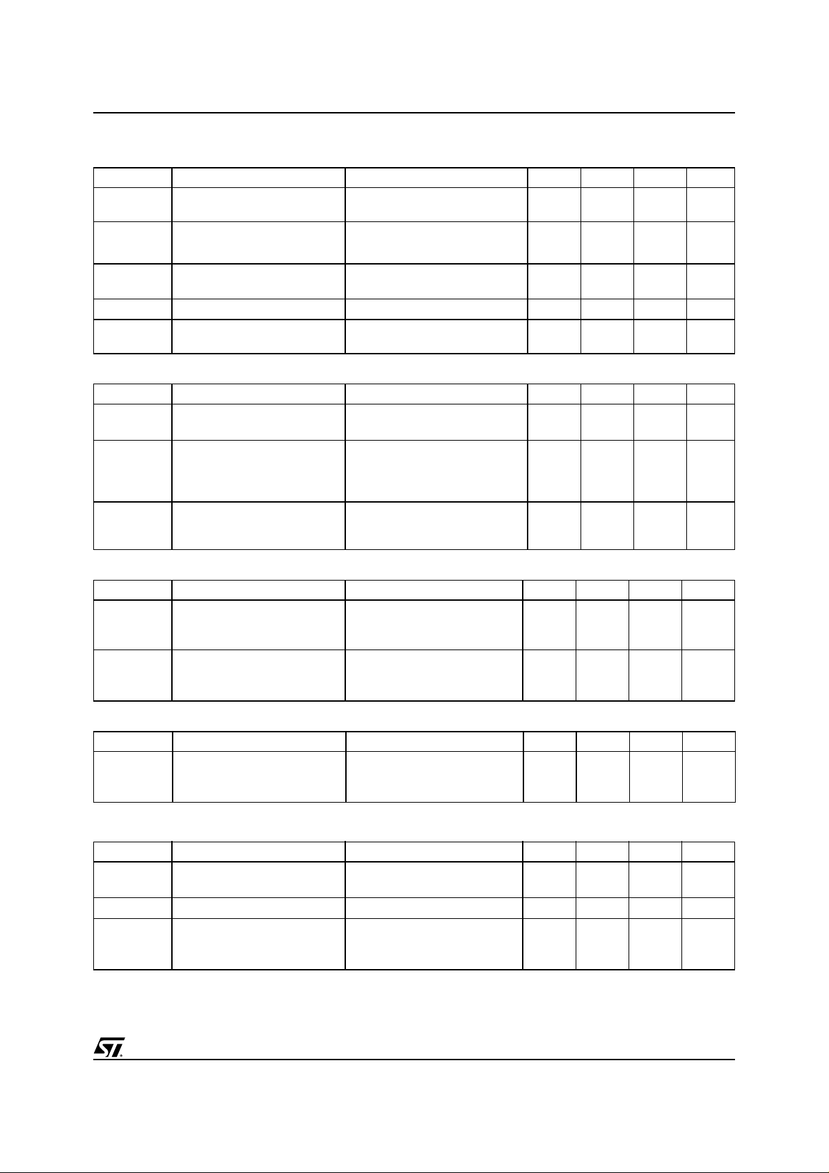
ABSOLUTE MAXIMUM RATINGS
Symbol Parameter Value Unit
V
DS
V
DGR
V
GS
I
D
I
D
I
DM
P
TOT
V
ESD(G-S)
dv/dt (1) Peak Diode Recovery voltage slope 15 V/ns
T
stg
T
j
(•)Pulse width limited by safe operating area
≤70A, di/dt ≤400 A/µs, VDD≤ V
(1) I
SD
THERMAL DATA
Rthj-case Thermal Resistance Junction-case Max 0.2 °C/W
Rthj-amb Thermal Resistance Junction-ambient Max 30 °C/W
T
l
Drain-source Voltage (VGS=0)
Drain-gate Voltage (RGS=20kΩ)
600 V
600 V
Gate- source Voltage ±30 V
Drain Current (continuous) at TC= 25°C
Drain Current (continuous) at TC= 100°C
()
Drain Current (pulsed) 280 A
Total Dissipation at TC= 25°C
70 A
44 A
600 W
Gate source ESD(HBM-C=100pF, R=15KΩ) 6KV
Derating Factor 4.5 W/°C
Storage Temperature –65 to 150 °C
Max. Operating Junction Temperature 150 °C
(BR)DSS,Tj≤TJMAX.
Maximum Lead Temperature For Soldering Purpose 300 °C
AVALANCHE CHARACTERISTICS
Symbol Parameter Max Value Unit
I
AR
E
AS
Avalanche Current, Repetitive or Not-Repetitive
(pulse width limited by T
max)
j
Single Pulse Avalanche Energy
(starting T
= 25 °C, ID=IAR,VDD=35V)
j
30 A
1.4 J
GATE-SOURCE ZENER DIODE
Symbol Parameter Test Conditions Min. Typ. Max. Unit
BV
GSO
Gate-Source Breakdown
Igs=± 1mA (Open Drain) 30 V
Voltage
PROTECTION FEATURES OF GATE-TO-SOURCE ZENER DIODES
The built-in back-to-back Zener diodes have specificall y b een des igned to enhance not only the device’s
ESD capability, but also to make them safely absorb possible voltage transients that may occasionally be
applied from gate to source. In this respect t he Zener voltage is appropriate to achie ve an ef fi cient and
cost-effective intervention to protect the device’s integrity. Th es e integrated Zener diodes thus avoid t he
usage of external components.
2/8
STE70NM60
ELECTRICAL CHARACTERISTICS (T
= 25 °C UNLESS O THERWISE SPECIFIED)
CASE
ON/OFF
Symbol Parameter Test Conditions Min. Typ. Max. Unit
V
(BR)DSS
Drain-source
ID= 250 µA, VGS= 0 600 V
Breakdown Voltage
I
DSS
I
GSS
V
GS(th)
R
DS(on)
Zero Gate Voltage
Drain Current (V
GS
=0)
Gate-body Leakage
Current (V
DS
=0)
Gate Threshold Voltage
Static Drain-source On
V
= Max Rating
DS
= Max Rating, TC= 125°C
V
DS
V
= ± 20V ±10 µA
GS
V
DS=VGS,ID
= 250 µA
34
10 µA
100 µA
5V
VGS=10V,ID= 30 A 0.050 0.055 Ω
Resistance
DYNAMIC
Symbol Parameter Test Conditions Min. Typ. Max. Unit
(1) Forward Transconductance VDS=I
g
fs
C
iss
C
oss
C
rss
R
G
Input Capacitance
Output Capacitance
Reverse Transfer
Capacitance
Gate Input Resistance f=1 MHz Gate DC Bias = 0
D(on)xRDS(on)max,
ID=30A
=25V,f=1MHz,VGS= 0 7300
V
DS
Test Signal Level = 20mV
Open Drain
35 S
2000
40
1.8 Ω
pF
pF
pF
SWITCHING ON
Symbol Parameter Test Conditions Min. Typ. Max. Unit
t
d(on)
Turn-on Delay Time
t
r
Rise Time
VDD=300V,ID=30A
= 4.7Ω VGS=10V
R
G
55
95
(see test circuit, Figure 3)
Q
g
Q
gs
Q
gd
Total Gate Charge
Gate-Source Charge
Gate-Drain Charge
VDD=470V,ID=60A,
VGS=10V
178
44.5
95
266 nC
SWITCHING OFF
Symbol Parameter Test Conditions Min. Typ. Max. Unit
t
r(Voff)
t
t
Off-voltage Rise Time
f
c
Fall Time
Cross-over Time
VDD= 400 V, ID=60A,
RG=4.7Ω, VGS=10V
(see test circuit, Figure 5)
130
76
105
SOURCE DRAIN DIODE
Symbol Parameter Test Conditions Min. Typ. Max. Unit
I
SD
I
SDM
VSD(1)
t
rr
Q
rr
I
RRM
Note: 1. Pulsed: Pulse duration = 300 µs, duty cycle 1.5 %.
2. Pulse width limited by safe operating area.
Source-drain Current
Source-drain Current (pulsed)
(2)
Forward On Voltage
Reverse Recovery Time
Reverse Recovery Charge
Reverse Recovery Current
ISD=60A,VGS=0
I
SD
VDD=30V,Tj= 150°C
(see test circuit, Figure 5)
= 60 A, di/dt = 100 A/µs,
600
14
48
60
240
1.5 V
ns
ns
nC
nC
ns
ns
ns
A
A
ns
µC
A
3/8
 Loading...