

STE53NA50
N - CHANNEL ENHANCEMENT MODE
FAST POWER MOS TRANSISTOR
TYPE V
DSS
R
DS(on)
I
D
STE53 NA 5 0 500 V < 0.085 Ω 53 A
■ TYPICALR
■ HIGH CURRENTPOWER MODULE
■ AVALANCHERUGGEDTECHNOLOGY
■ VERYLARGE SOA - LARGE PEAKPOWER
DS(on)
=0.075 Ω
CAPABILITY
■ EASY TO MOUNT
■ SAME CURRENTCAPABILITYFOR THE
TWOSOURCE TERMINALS
■ EXTREMELY LOW Rth (Junction to case)
■ VERYLOW INTERNAL PARASITIC
INDUCTANCE
■ ISOLATEDPACKAGEULRECOGNIZED
APPLICATIONS
■ SMPS & UPS
■ MOTORCONTROL
■ WELDINGEQUIPMENT
■ OUTPUTSTAGE FOR PWM, ULTRASONIC
CIRCUITS
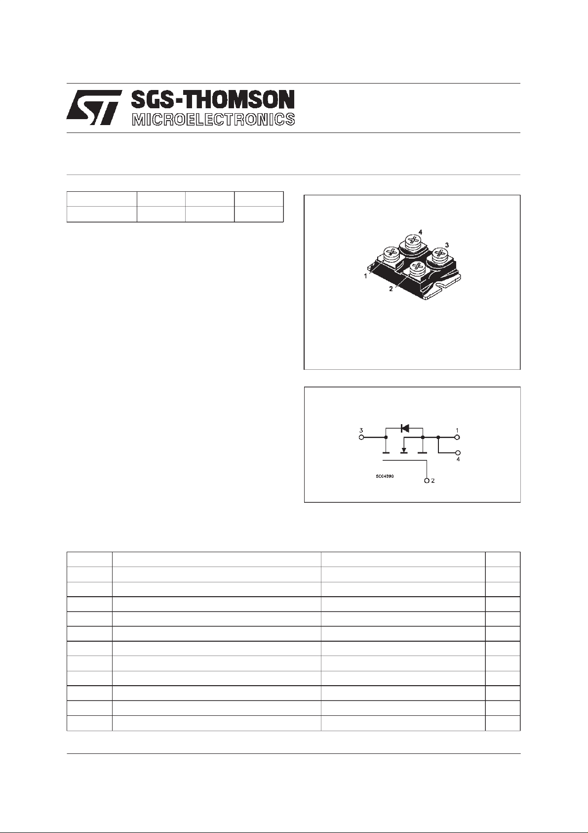
ISOTOP
INTERNAL SCHEMATIC DIAGRAM
ABSOLUTE MAXIMUM RATINGS
Symbol Parameter Value Unit
V
V
V
I
DM
P
T
V
(•) Pulsewidth limited by safe operating area
February 1998
Drain-sourc e V ol t ag e (VGS=0) 500 V
DS
DGR Drain- g at e Voltage ( R
Gate- source Voltage ± 30 V
GS
I
Drain Current (con t inuous) a t Tc=25oC53A
D
I
Drain Current (con t inuous) a t Tc=100oC33A
D
=20kΩ)
GS
500 V
(•) Drain Current (pulsed) 212 A
Total Dissipation at Tc=25oC460W
tot
Derating Fa c tor 3.68 W/
St orage T emperat ure -55 to 150
stg
T
Max. O pera ting Junction T emperat ure 150
j
Insulation Withhstand Voltage (AC-RMS) 2500 V
ISO
o
C
o
C
o
C
1/7
STE53NA50
THERMAL DATA
R
thj-case
R
thc-h
AVALANCHE CHARACTERISTICS
Symbol Para met e r Max Value Uni t
I
AR
E
Ther mal Resist ance Junctio n-case Max
Ther mal Resist ance Case-heat si nk With Cond uctive
Gr ease Ap plied Max
Avalanche Cur rent, Repet it i v e or Not-Re petitive
(pulse w idth limited by T
Single Pulse Avalanche Energy
AS
(starting T
=25oC, ID=IAR,VDD=50V)
j
max, δ <1%)
j
0.27
0.05
26 A
1014 mJ
o
C/W
o
C/W
ELECTRICAL CHARACTERISTICS (T
=25oC unlessotherwise specified)
case
OFF
Symbol Parameter Test Condition s Min. Typ. Max. Un it
V
(BR)DSS
Drain-sourc e
ID=1mA VGS= 0 500 V
Breakdown V oltage
I
I
DSS
GSS
Zer o Gat e Vo lt age
Drain Current (V
GS
Gat e-body Leaka ge
Current (V
DS
=0)
=0)
V
=MaxRating
DS
=MaxRating Tc=125oC
V
DS
= ± 30 V
V
GS
100
1000µAµA
± 400 nA
ON (∗)
Symbol Parameter Test Condition s Min. Typ. Max. Un it
V
GS(th )
Gate Threshold
VDS=VGSID=1mA 2.25 3 3.75 V
Voltage
R
DS(on)
Stati c Drain-so urce On
VGS=10V ID= 27 A 0.075 0.085 Ω
Resistance
I
D(on)
On State Drain Current VDS>I
D(on)xRDS(on)max
53 A
VGS=10V
DYNAMIC
Symbol Parameter Test Condition s Min. Typ. Max. Un it
g
(∗)Forward
fs
Tr ansconductanc e
C
C
C
Input Capac i t an c e
iss
Out put Capa c itance
oss
Reverse Transf er
rss
Capa cit an c e
VDS>I
D(on)XRDS(o n)MAXID
=27A 25 S
VDS=25V f=1MHz VGS=0 13
1500
450
16
2000
650
nF
pF
pF
2/7
STE53NA50
ELECTRICAL CHARACTERISTICS (continued)
SWITCHINGON
Symbol Parameter Test Condition s Min. Typ. Max. Un it
t
d(on)
t
r
Turn-on Time
Rise Tim e
VDD=250V ID=27A
=4.7 Ω VGS=10V
R
G
57
92
(see test circuit, figure 1)
Q
Q
Q
Total Gate Charge
g
Gat e-Sour ce Cha rge
gs
Gate-Drain Charge
gd
VDD=400V ID=53A VGS= 10 V 470
54
219
SWITCHINGOFF
Symbol Parameter Test Condition s Min. Typ. Max. Un it
t
r(Voff)
t
t
Of f - voltage Rise Time
Fall Time
f
Cross-ov er Time
c
VDD=400V ID=53A
=4.7 Ω VGS=10V
R
G
(see test circuit, figure 3)
105
36
145
SOURCE DRAIN DIODE
Symbol Parameter Test Condition s Min. Typ. Max. Un it
I
SD
I
SDM
V
SD
t
Q
I
RRM
(∗) Pulsed: Pulse duration =300 µs, duty cycle 1.5 %
(•) Pulse widthlimited by safeoperating area
Source-drain Curre nt
(•)
Source-drain Curre nt
(pulsed)
(∗) Forwar d On Vo lt age ISD=53A VGS=0 1.6 V
Reverse Recov er y
rr
Time
Reverse Recov er y
rr
= 53 A di/d t = 100 A/µs
I
SD
=100V Tj=150oC
V
R
(see test circuit, figure 3)
1000
31.5
Charge
Reverse Recov er y
63
Current
80
130
658 nC
145
50
205
53
212
ns
ns
nC
nC
ns
ns
ns
A
A
ns
µC
A
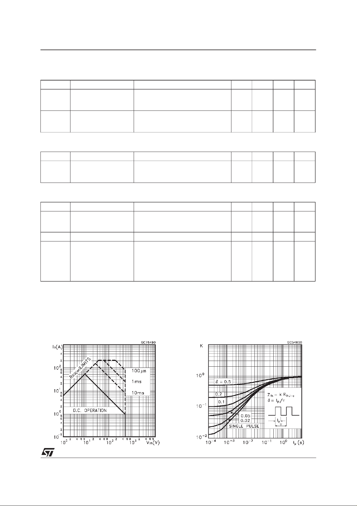
Safe Operating Areafor ThermalImpedance
3/7

STE53NA50
OutputCharacteristics
Transconductance
TransferCharacteristics
StaticDrain-sourceOn Resistance
GateCharge vs Gate-sourceVoltage
4/7
CapacitanceVariations

STE53NA50
Normalized GateThresholdVoltage vs
Temperature
Source-drainDiode Forward Characteristics
Normalized On Resistancevs Temperature
Fig. 1: Switching Times Test Circuits For
Resistive Load
Fig. 2: GateCharge test Circuit
Fig. 3: TestCircuit For InductiveLoad Switching
AndDiode RecoveryTimes
5/7

STE53NA50
ISOTOPMECHANICAL DATA
DIM.
MIN. TYP. MAX. MIN. TYP. MAX.
A 11.8 12.2 0.466 0.480
B 8.9 9.1 0.350 0.358
C 1.95 2.05 0.076 0.080
D 0.75 0.85 0.029 0.033
E 12.6 12.8 0.496 0.503
F 25.15 25.5 0.990 1.003
G 31.5 31.7 1.240 1.248
H 4 0.157
J 4.1 4.3 0.161 0.169
K 14.9 15.1 0.586 0.594
L 30.1 30.3 1.185 1.193
M 37.8 38.2 1.488 1.503
N 4 0.157
O 7.8 8.2 0.307 0.322
mm inch
G
A
B
O
N
D
E
F
H
J
C
K
L
M
6/7

STE53NA50
Information furnished is believed tobe accurate and reliable. However, SGS-THOMSON Microelectronics assumes no responsability for the
consequences of use of such information nor for any infringement of patents orother rightsof third parties which may results from itsuse. No
license is granted by implication or otherwiseunder any patent orpatent rightsofSGS-THOMSON Microelectronics. Specifications mentioned
in thispublication are subjectto change without notice.This publication supersedes and replaces all information previously supplied.
SGS-THOMSON Microelectronics productsare not authorizedfor use as critical componentsin life support devicesor systems withoutexpress
written approval ofSGS-THOMSON Microelectonics.
1998 SGS-THOMSONMicroelectronics - Printed in Italy - All RightsReserved
Australia - Brazil - Canada - China - France - Germany - Italy - Japan - Korea- Malaysia - Malta - Morocco - The Netherlands -
Singapore - Spain- Sweden - Switzerland- Taiwan - Thailand - United Kingdom - U.S.A
SGS-THOMSON MicroelectronicsGROUP OF COMPANIES
...
7/7
 Loading...