


查询STE50DE100供应商
HYBRID EMITTER SWITCHED BIPOLAR TRANSISTOR
ESBT™ 1000 V - 50 A - 0.026 W POWER MODULE
STE50DE100
Table 1: General Features
V
CS(ON)
1.3 V 50 A 0.026 W
n HIGH VOLTAGE / HIGH CURRENT
I
C
R
CS(ON)
CASCODE CONFIGURATION
n ULTRA LOW EQUIVALENT ON
RESISTANCE
n VERY FAST-SWITCH, UP TO 150 kHz
n ULTRA LOW C
n LOW DYNAMIC V
ISS
CS(ON)
APPLICATION
n INDUSTRIAL CONVERTERS
n WELDING
DESCRIPTION
The STE50DE100 is manufactured in a hybrid
structure, using dedicated high voltage Bipolar
and low voltage MOSFET technologies, aimed to
providing the best performance in ESBT topology.
The STE50DE100 is designed for use in industrial
converters and/or welding equipment.
Figure 1: Package
ISOTOP
Figure 2: Internal Schematic Diagram
Electrical Symbol Device Structure
Table 2: Order Code
Part Number Marking Package Packaging
STE50DE100 STE50DE100 ISOTOP TUBE
Rev. 1
1/9October 2004

STE50DE100
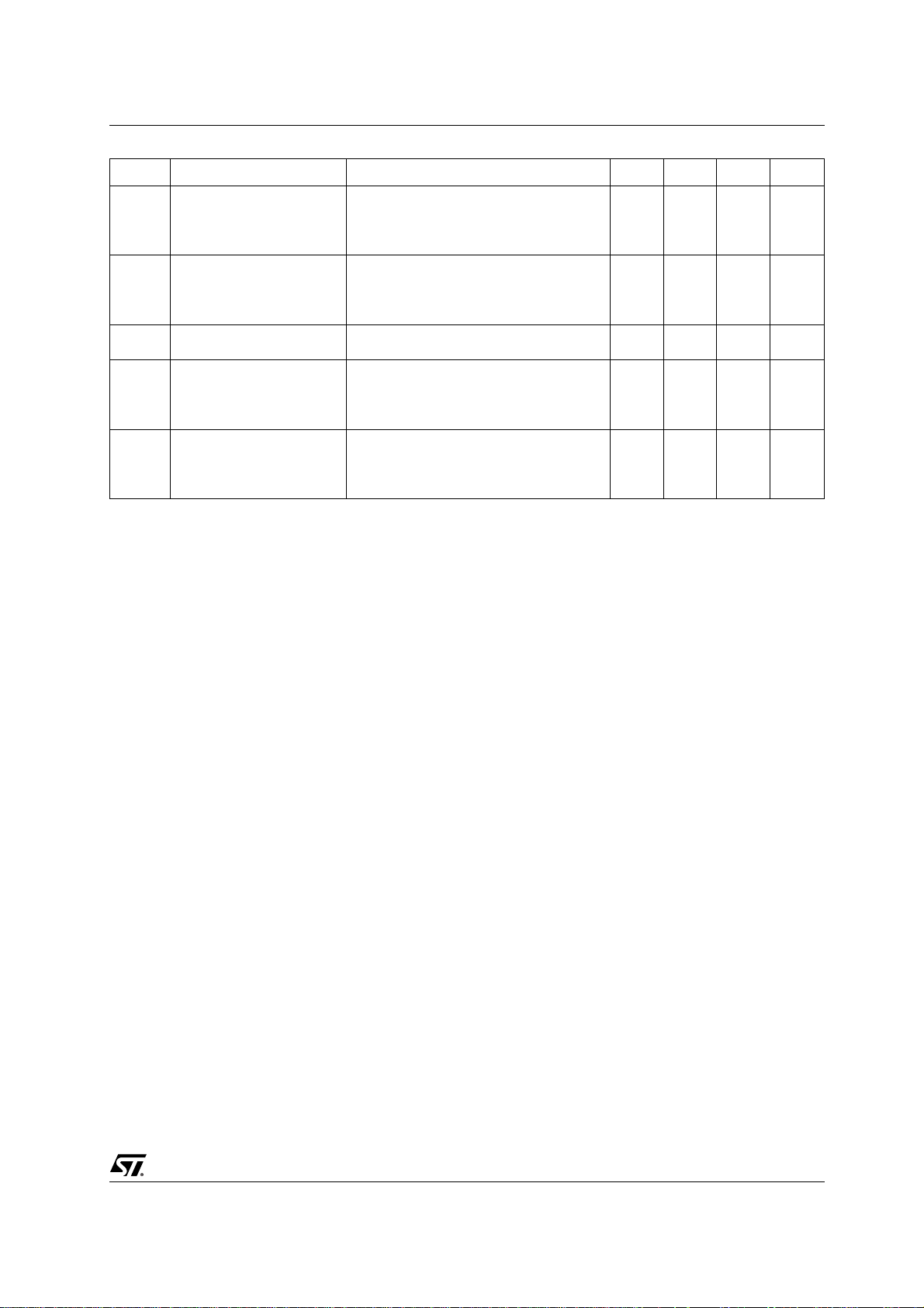
Table 3: Absolute Maximum Ratings
Symbol Parameter Value Unit
V
CS(SS)
V
BS(OS)
V
SB(OS)
V
I
I
CM
I
I
BM
P
T
T
V
ISO
Table 4: Thermal Data
R
thj-case
R
thc-h
Collector-Source Voltage (VBS = VGS = 0 V)
Base-Source Voltage (IC= 0, VGS = 0 V)
Source-Base Voltage (IC= 0, VGS = 0 V)
Gate-Source Voltage
GS
Collector Current
C
Collector Peak Current (tp < 5ms)
Base Current
B
Base Peak Current (tp < 1ms)
Total Dissipation at TC ≤ 25 oC
tot
Storage Temperature
stg
Max. Operating Junction Temperature
J
Insulation Withstand Voltage (AC-RMS) from All Four Leads to
External Heatsink
Thermal Resistance Junction-Case Max
Thermal Resistance Case-heatsink with Conductive Grease
Applied Max
1000 V
40 V
12 V
± 20 V
50 A
150 A
10 A
50 A
160 W
-65 to 150 °C
150 °C
2500 V
0.78
0.05
o
C/W
o
C/W
Table 5: Electrical Characteristics (T
= 25 oC unless otherwise specified)
case
Symbol Parameter Test Conditions Min. Typ. Max. Unit
I
CS(SS)
I
BS(OS)
I
SB(OS)
I
GS(OS)
V
CS(ON)
Collector-Source Current
(V
= VGS = 0 V)
BS
Base-Source Current
(I
= 0 , VGS = 0 V)
C
Source-Base Current
(I
= 0 , VGS = 0 V)
C
V
V
V
= 1000 V 100 mA
CS(SS)
= 40 V 10 mA
BS(OS)
= 10 V 100 mA
SB(OS)
Gate-Source Leakage VGS = ± 20 V 500 nA
Collector-Source ON
Voltage
IC = 50 A IB = 10 A VGS = 10 V
I
= 30 A IB = 3 A VGS = 10 V
C
1.3
1.1
(see figure 14)
h
V
BS(ON)
V
GS(th)
C
Q
GS(tot)
DC Current Gain IC = 50 A VCS = 1 V VGS = 10 V
FE
I
= 30 A VCS = 1 V VGS = 10 V
C
Base-Source ON Voltage IC = 50 A IB = 10 A VGS = 10 V
I
= 30 A IB = 3 A VGS = 10 V
C
Gate Threshold Voltage VBS = VGS IB = 250 mA33.74.5V
Input Capacitance VCS = 25 V f = 1MHZ
iss
V
= VCB = 0
GS
Gate-Source Charge VCS = 25 V VGS = 10 V
V
= 0 IC = 50 A
CB
3
6
2.2
1.4
2500 pF
60 nC
7
13
V
V
V
V
2/9
STE50DE100
Symbol Parameter Test Conditions Min. Typ. Max. Unit
t
t
V
CSW
V
CS(dyn)
V
CS(dyn)
INDUCTIVE LOAD
Storage Time
s
t
Fall Time
f
INDUCTIVE LOAD
Storage Time
s
t
Fall Time
f
Maximum Collector-Source
Voltage without Snubber
Collector-Source Dynamic
Voltage
(500 ns)
Collector-Source Dynamic
Voltage
(1ms)
VGS = 10 V V
R
= 47 W tp = 4 ms
G
I
= 25 A IB = 5 A (see figure 15)
C
VGS = 10 V V
R
= 47 W tp = 4 ms
G
I
= 25 A IB = 2.5 A (see figure 15)
C
Clamp
Clamp
= 800 V
= 800 V
0.65
10
0.43
6
ms
ms
RG = 47 W hFE = 5 A IC = 35 A 1000 V
VCC = V
R
= 47 W IB = 5 A
G
I
= IC = 25 A t
Bpeak
VCC = V
R
= 47 W IB = 5 A
G
I
= IC = 25 A t
Bpeak
= 300 V VGS = 10 V
Clamp
= 300 V VGS = 10 V
Clamp
peak
peak
5.5 V
= 500 ns
4.8 V
= 500 ns
ns
ns
3/9

STE50DE100
Figure 3: Output Characteristics
Figure 4: Reverse Biased Safe Operating Area
Figure 6: Gate Threshold Voltage vs Temperature
Figure 7: Dynamic Collector-Emitter Saturation Voltage
Figure 5: DC Current Gain
4/9

STE50DE100
Figure 8: Collector-Source On Voltage
Figure 9: Base-Source On Voltage
Figure 11: Collector-Source On Voltage
Figure 12: Base-Source On Voltage
Figure 10: Inductive Load Switching Time
Figure 13: Inductive Load Switching Time
5/9

STE50DE100
Figure 14: Static V
CS(ON)
Test Circuit
Figure 15: Inductive Load Switching and RBSOA Test Circuit
Figure 16: Inductive Load Turn-on Switching and Dynamic V
6/9
CS(ON)
Test Circuit

ISOTOP MECHANICAL DATA
STE50DE100
DIM.
MIN. TYP. MAX. MIN. TYP. MAX.
A 11.8 12.2 0.466 0.480
B 8.9 9.1 0.350 0.358
C 1.95 2.05 0.076 0.080
D 0.75 0.85 0.029 0.033
E 12.6 12.8 0.496 0.503
F 25.15 25.5 0.990 1.003
G 31.5 31.7 1.240 1.248
H4 0.157
J 4.1 4.3 0.161 0.169
K 14.9 15.1 0.586 0.594
L 30.1 30.3 1.185 1.193
M 37.8 38.2 1.488 1.503
N4 0.157
O 7.8 8.2 0.307 0.322
mm inch
G
A
N
O
B
D
E
F
H
J
K
L
M
C
7/9
STE50DE100
Table 6: Revision History
Date Release Change Designator
06-Oct-2004 1 First Release.
8/9

STE50DE100
Information furnished is believed to be accurate and reliable. However, STMicroelectronics assumes no responsibility for the consequences
of use of suc h inf ormati on nor for a ny i nfr ingeme nt o f p atents or other rights of third parties which m ay res ult fr om i ts us e. No li cens e i s gr an ted
by implication or otherwise under any patent or patent rights of STMicroelectronics. Specifications mentioned in this publication are subject
to change without notice. This publication s u persedes and replaces all information previously supplied. STMicroelectronics products are not
authorized for use as critical components in life support devices or systems without express written approval of STMicroelectronics.
The ST logo is a registered trademark of STMicroelectronics
All other names are the property of their respective owners
© 2004 STMicroelectronics - All Rights Reserved
STMicroelectronics group of companies
Australia - Belgium - Brazil - Canada - China - Czech Republic - Finland - France - Germany - Hong Kong - India - Israel - Italy - Japan -
Malaysia - Malta - Morocco - Singapore - Spain - Sweden - Switzerland - United Kingdom - United States of America
www.st.com
9/9
 Loading...