

ST STE40NK90ZD User Manual
查询STE40NK90ZD供应商
STE40NK90ZD
N-CHANNEL 900V - 0.14Ω - 40 A ISOTOP
Super FREDMesh™ MOSFET
Table 1: Ge neral Features
TYPE V
STE40NK90ZD 900 V < 0.18 Ω 40 A 600 W
■ TYPICAL R
■ EXTREMELY HIGH dv/d t C APABILITY
■ 100% AVALANCHE TESTED
■ GATE CHARGE MINIMIZED
■ VERY LOW INTRINSIC CAPACITANCES
■ VERY GOOD MANUFACTURING
DSS
(on) = 0.14 Ω
DS
R
DS(on)
I
Pw
D
REPEATIBILITY
DESCRIPTION
The SuperFREDMesh™ series is obtained
through an extreme optimization of ST’s well established strip-based PowerMESH™ layout. In addition to pushing on-resistance significantly down,
special care is taken to ensure a very good dv/dt
capability for the most demanding applications.
Such series complements ST full range of high
voltage MOSFETs including revolutionary MDmesh™ products.
APPLICATIONS
■ HIGH CURRENT, HIGH SPEED SWITCHING
■ IDEAL FOR WELDING EQUIPMENT
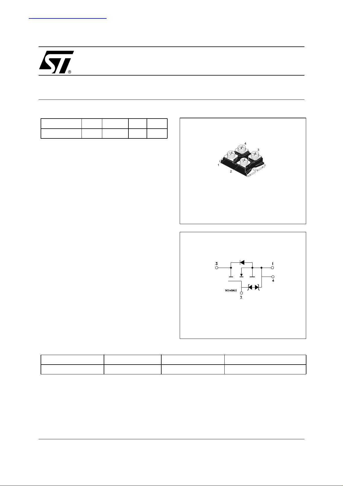
Figure 1: Package
ISOTOP
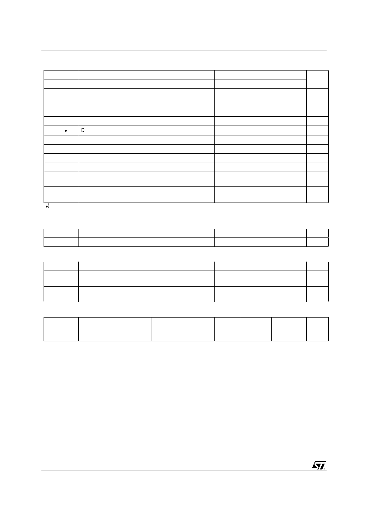
Figure 2: Internal Schematic Diagram
Table 2: Order Codes
SALES TYPE MARKING PACKAGE PACKAGING
STE40NK90ZD E40NK90ZD ISOTOP TUBE
Rev. 4
1/10December 2004
STE40NK90ZD
Table 3: Absolute Maximum ratings
Symbol Parameter Value Unit
V
DS
V
DGR
V
GS
I
D
I
D
I
DM
P
TOT
V
ESD(G-S)
dv/dt (1) Peak Diode Recovery voltage slope 8 V/ns
V
ISO
T
j
T
stg
() Pulse width limited by safe operating area
≤ 40A, di/dt ≤ 500 A/µs, VDD ≤ V
(1) I
SD
Table 4: Thermal Data
Rthj-case Thermal Resistance Junction-case Max 0.2 °C/W
Rthj-amb Thermal Resistance Junction-ambient Max 40 °C/W
Drain-source Voltage (VGS = 0)
Drain-gate Voltage (RGS = 20 kΩ)
900 V
900 V
Gate- source Voltage ± 30 V
Drain Current (continuous) at TC = 25°C
Drain Current (continuous) at TC = 100°C
()
Drain Current (pulsed) 160 A
Total Dissipation at TC = 25°C
40 A
25 A
600 W
Derating Factor 5 W/°C
Gate source ESD(HBM-C=100pF, R=1.5KΩ) 7KV
Insulation Withstand Voltage (AC-RMS) from All Four
2500 V
Terminals to External Heatsink
Operating Junction Temperature
Storage Temperature
.
(BR)DSS
- 65 to 150 °C
Table 5: Avalanche Characteristics
Symbol Parameter Max. Value Unit
I
AR
E
AS
Avalanche Current, Repetitive or Not-Repetitive
(pulse width limited by T
max)
j
Single Pulse Avalanche Energy
(starting T
= 25 °C, ID = IAR, VDD = 35 V)
j
40 A
1.2 J
Table 6: Gate-Source Zener Diode
Symbol Parameter Test Conditions Min. Typ. Max. Unit
BV
GSO
Gate-Source Breakdown
Igs=± 1mA (Open Drain) 30 V
Voltage
PROTECTION FEATURES OF GATE-TO-SOURCE ZENER DIODES
The built-in back-to-back Zener diodes have specifically been designed to enhance not only the device’s
ESD capability, but also to make them safely absorb possible voltage transients that may occasionally be
applied from gate to source. In this respect the Zener voltage is appropriate to achieve an efficient and
cost-effective intervention to protect the device’s integrity. These integrated Zener diodes thus avoid the
usage of external components.
2/10
STE40NK90ZD
ELECTRICAL CHARACTERISTICS (T
=25°C UNLESS OTHERWISE SPECIFIED)
CASE
Table 7: On/Off
Symbol Parameter Test Conditions Min. Typ. Max. Unit
V
(BR)DSS
Drain-source
ID = 1 mA, VGS = 0 900 V
Breakdown Voltage
I
I
V
GS(th)
R
DS(on)
DSS
GSS
Zero Gate Voltage
Drain Current (V
GS
= 0)
Gate-body Leakage
Current (V
DS
= 0)
Gate Threshold Voltage
Static Drain-source On
V
= Max Rating
DS
V
= Max Rating, TC = 125 °C
DS
V
= ± 20V ±10 µA
GS
V
= VGS, ID = 150µA
DS
2.5 3.75 4.5 V
10
100
VGS = 10V, ID = 20 A 0.14 0.18 Ω
Resistance
Table 8: Dynamic
Symbol Parameter Test Conditions Min. Typ. Max. Unit
(1) Forward Transconductance VDS = 15V, ID=20 A 35 S
g
fs
C
oss eq.
C
C
C
t
d(on)
t
d(off)
Q
Q
Q
iss
oss
rss
t
r
t
gs
gd
f
Input Capacitance
Output Capacitance
Reverse Transfer
Capacitance
(3) Equivalent Output
Capacitance
Turn-on Delay Time
Rise Time
Turn-off Delay Time
Fall Time
Total Gate Charge
g
Gate-Source Charge
Gate-Drain Charge
= 25V, f = 1 MHz, VGS = 0 25000
V
DS
1450
280
VGS = 0V, VDS = 0V to 720V 720 pF
= 450 V, ID = 18 A
V
DD
R
=4.7Ω , VGS = 10 V
G
(Figure 17)
92
102
450
200
= 720 V, ID = 36 A,
V
V
DD
GS
= 10V
590
89
826 nC
323
µA
µA
pF
pF
pF
ns
ns
ns
ns
nC
nC
Table 9: Source Drain Diode
Symbol Parameter Test Conditions Min. Typ. Max. Unit
I
SD
I
SDM
(1)
V
SD
t
rr
Q
rr
I
RRM
t
rr
Q
rr
I
RRM
Note: 1. Pulsed: Pu l se duration = 300 µs, duty cyc l e 1.5 %.
2. Pulse width limited by safe operating area.
3. C
Source-drain Current
(2)
Source-drain Current (pulsed)
Forward On Voltage
Reverse Recovery Time
Reverse Recovery Charge
Reverse Recovery Current
Reverse Recovery Time
Reverse Recovery Charge
Reverse Recovery Current
ISD = 40 A, VGS = 0
I
SD
V
DD
(Figure 18)
I
SD
V
DD
(Figure 18)
is defined as a constant equivalent capacitance giving the same charging time as C
oss eq.
.
V
DSS
= 36 A, di/dt = 100 A/µs
= 50 V, Tj = 25°C
= 36 A, di/dt = 100 A/µs
= 50 V, Tj = 150°C
450
3.6
16.2
930
12
26
when VDS increases fr om 0 to 80%
oss
40
160
1.6 V
A
A
ns
µC
A
ns
µC
A
3/10
 Loading...