

N - CHANNEL ENHANCEMENT MODE
FAST POWER MOS TRANSISTOR
TYPE V
DSS
STE40 NA 6 0 600 V < 0 .135 Ω 40 A
R
DS(on)
I
D
STE40NA60
PRELIMINARY DATA
■ TYPICALR
■ HIGH CURRENTPOWER MODULE
■ AVALANCHERUGGEDTECHNOLOGY
■ VERYLARGE SOA - LARGE PEAK POWER
DS(on)
=0.12 Ω
CAPABILITY
■ EASY TO MOUNT
■ SAME CURRENTCAPABILITYFOR THE
TWOSOURCE TERMINALS
■ EXTREMELY LOW Rth (Junctionto case)
■ VERYLOW INTERNAL PARASITIC
INDUCTANCE
■ ISOLATEDPACKAGEULRECOGNIZED
APPLICATIONS
■ SMPS & UPS
■ MOTORCONTROL
■ WELDINGEQUIPMENT
■ OUTPUTSTAGE FOR PWM,ULTRASONIC
CIRCUITS
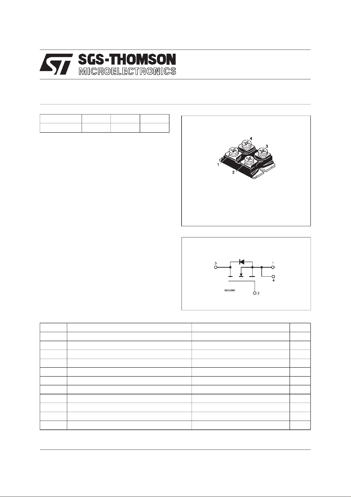
ISOTOP
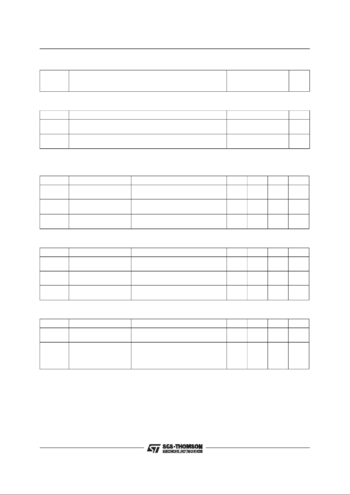
INTERNAL SCHEMATIC DIAGRAM
ABSOLUTE MAXIMUM RATINGS
Symbol Parameter Value Unit
V
V
V
I
DM
P
T
V
(•) Pulsewidth limited by safe operatingarea
January 1998
Drain-sourc e V ol t ag e (VGS=0) 600 V
DS
Drain- g at e Voltage (RGS=20kΩ)
DGR
Gate- source Voltage ± 30 V
GS
I
Drain Current (con t inuous) a t Tc=25oC40A
D
I
Drain Current (con t inuous) a t Tc=100oC26A
D
600 V
(•) Drain Current (pulsed) 160 A
Total Dissipation at Tc=25oC460W
tot
Derating Factor 3.6 W/
St orage Temperatur e -55 to 15 0
stg
T
Max. Operating Junction T empe rature 150
j
Insulation Withhstand Voltage (AC-RMS) 2500 V
ISO
o
C
o
C
o
C
1/5
STE40NA60
THERMAL DATA
R
thj-case
R
thc-h
AVALANCHE CHARACTERISTICS
Symbol Para met e r Max Value Uni t
I
AR
E
Ther mal Resist ance Junctio n-case Max
Ther mal Resist ance Case-heat si nk With C ond uctive
Gr ease A p plied M ax
Avalanche Cur rent, Repet it i v e or Not-Re petitive
(pulse width lim ited b y T
Single Pulse Avalanche Energy
AS
(starting T
=25oC, ID=IAR,VDD=50V)
j
max, δ <1%)
j
0.27
0.05
20 A
3000 mJ
o
C/W
o
C/W
ELECTRICAL CHARACTERISTICS (T
=25oC unlessotherwise specified)
case
OFF
Symbol Parameter Test Cond itions Min. Typ. Max. Unit
V
(BR)DSS
Drain-sourc e
=500µAVGS=0
I
D
900 V
Breakdown V oltage
I
I
DSS
GSS
Zer o Gat e V o lt age
Drain Current (V
GS
Gat e-body Leaka ge
Current (V
DS
=0)
=0)
V
=MaxRating
DS
=0.8x Max Rating Tc= 125oC
V
DS
= ± 30 V
V
GS
250
1000µAµA
± 200 nA
ON (∗)
Symbol Parameter Test Cond itions Min. Typ. Max. Unit
V
GS(th )
Gate Threshold
VDS=VGSID=1mA 2.25 3 3.75 V
Voltage
R
DS(on)
Stati c D rain-source On
VGS=10V ID= 2 0 A 0.12 0. 1 35 Ω
Resistance
I
D(on)
On State Drain Curre nt VDS>I
D(on)xRDS(on)max
40 A
VGS=10V
DYNAMIC
Symbol Parameter Test Cond itions Min. Typ. Max. Unit
g
(∗)Forward
fs
Tr ansconductanc e
C
C
C
Input Capac i t an c e
iss
Out put C apa c itance
oss
Reverse Transf er
rss
Capa cit an c e
VDS>I
D(on)xRDS(on)maxID
=20A 20 S
VDS=25V f=1.0MHz VGS= 0 13000
1500
350
16000
1700
450
pF
pF
pF
2/5

STE40NA60
ELECTRICAL CHARACTERISTICS (continued)
SWITCHINGON
Symbol Parameter Test Cond itions Min. Typ. Max. Unit
t
d(on)
Q
Q
Q
Turn-on Time
Rise Tim e
t
r
Total Gate Charge
g
Gat e-Sour ce Cha rge
gs
Gate-Drain Charge
gd
VDD=300V ID=20A
=4.7 Ω VGS=10V
R
G
VDD=480V ID=40A VGS= 1 0 V 460
55
95
48
217
SWITCHINGOFF
Symbol Parameter Test Cond itions Min. Typ. Max. Unit
t
r(Voff)
t
t
Of f - voltage Rise Time
Fall Time
f
Cross-ov er Time
c
VDD=480V ID=40A
=4.7 Ω VGS=10V
R
G
95
30
140
SOURCE DRAIN DIODE
Symbol Parameter Test Cond itions Min. Typ. Max. Unit
I
SD
I
SDM
V
SD
t
Q
I
RRM
(∗) Pulsed: Pulse duration =300 µs, duty cycle1.5 %
(•) Pulse width limited by safe operating area
Source-drain Curre nt
(•)
Source-drain Curre nt
(pulsed)
(∗) Forwar d On V o lt age ISD=40A VGS=0 1.6 V
Reverse Recov er y
rr
Time
Reverse Recov er y
rr
= 4 0 A di/dt = 10 0 A/µs
I
SD
=100V Tj=150oC
V
R
1050
31.5
Charge
Reverse Recov er y
60
Current
75
125
600 nC
125
40
180
40
160
ns
ns
nC
nC
ns
ns
ns
A
A
ns
µC
A
3/5

STE40NA60
ISOTOPMECHANICAL DATA
DIM.
MIN. TYP. MAX. MIN. TYP. MAX.
A 11.8 12.2 0.466 0.480
B 8.9 9.1 0.350 0.358
C 1.95 2.05 0.076 0.080
D 0.75 0.85 0.029 0.033
E 12.6 12.8 0.496 0.503
F 25.15 25.5 0.990 1.003
G 31.5 31.7 1.240 1.248
H 4 0.157
J 4.1 4.3 0.161 0.169
K 14.9 15.1 0.586 0.594
L 30.1 30.3 1.185 1.193
M 37.8 38.2 1.488 1.503
N 4 0.157
O 7.8 8.2 0.307 0.322
mm inch
G
A
B
O
N
D
E
F
H
J
C
K
L
M
4/5

STE40NA60
Information furnished is believed to be accurate and reliable. However, SGS-THOMSON Microelectronics assumes no responsability for the
consequences of use of such information nor for any infringement of patents or other rights of third parties which may results from its use. No
license is granted by implication or otherwise under any patent orpatent rights of SGS-THOMSON Microelectronics. Specifications mentioned
in thispublication are subjectto change without notice. This publication supersedesand replaces all information previously supplied.
SGS-THOMSON Microelectronics productsare not authorizedfor use as critical componentsin life support devicesor systems withoutexpress
written approval ofSGS-THOMSON Microelectonics.
1998 SGS-THOMSON Microelectronics - Printed in Italy - All Rights Reserved
Australia - Brazil - Canada - China - France - Germany - Italy - Japan - Korea - Malaysia - Malta - Morocco - The Netherlands -
Singapore - Spain - Sweden - Switzerland - Taiwan - Thailand - United Kingdom - U.S.A
SGS-THOMSON Microelectronics GROUP OF COMPANIES
...
5/5
 Loading...