

®
STE38NB50
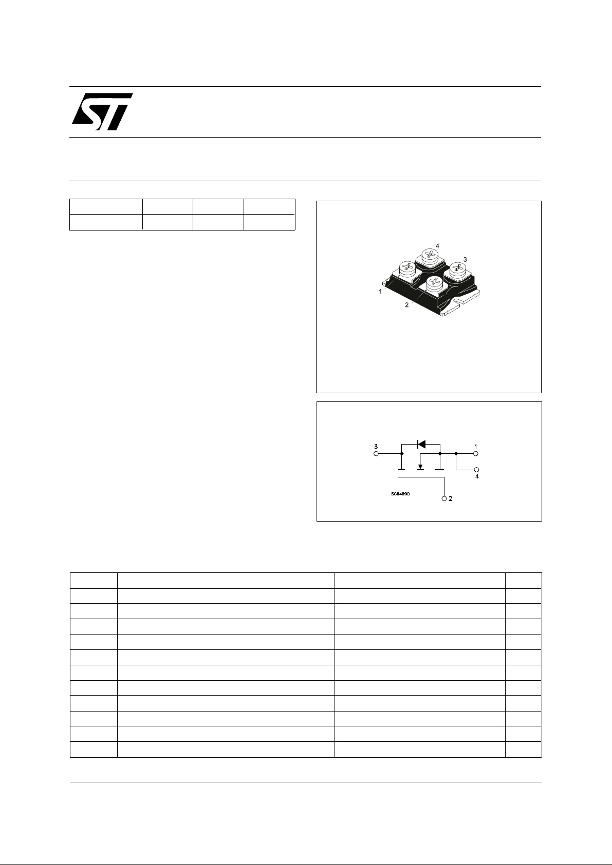
N - CHANNEL 500V - 0.11 Ω - 38A - ISOTOP
PowerMESH MOSFET
TYPE V
DSS
R
DS(on)
I
D
STE38NB50 500 V < 0.13 Ω 38 A
■ TYPICAL R
■ EXTREMELY HIGH dv/dt CAPABILITY
■ ± 30V GATE TO SOURCE VOLTA GE RATING
■ 100% AVALANCHE TESTED
■ LOW INTRINSIC CAPACITANCE
■ GATE CH ARGE MINIMIZED
■ REDUCED VOLTAGE SPRE AD
DS(on)
= 0.11 Ω
DESCRIPTIO N
Using the latest high voltage MESH OVERLAY
process, SGS-Thomson has designed an advanced family of power MOSFETs with outstanding performances. The new patent pending strip
layout coupled with the Company’s proprietary
edge termination structure, gives the lowest
RDS(on) per area, exceptional avalanche and
dv/dt capabilities and unrivalled gate charge and
switching characteristic s.
APPLICATIONS
■ HIGH CURRENT, HIGH SPE ED SWI TCHING
■ SWITCH MODE P OW ER SUP P LY (S MP S)
■ DC-AC CONVERTER FOR W ELDING
EQUIPMENT AND UNINTERRUPTABLE
POWER SU PPLY AND MOTOR DRIV E
ISOTOP
INTERNAL SCHEMATIC DIAGRAM
ABSOL UT E MAXIMU M RATINGS
Symbol Parameter Value Unit
V
V
V
I
DM
P
dv/dt(1) Peak Diode Recovery voltage slope 4.5 V/ns
T
(•) Pulse width limited by safe operating area (1) ISD ≤38 A, di/dt ≤ 200 A/µs, VDD ≤ V
June 1998
Drain-source Voltage (VGS = 0) 500 V
DS
Drain- gate Voltage (RGS = 20 kΩ) 500 V
DGR
Gate-source Voltage ± 30 V
GS
I
Drain Current (continuous) at Tc = 25 oC38A
D
I
Drain Current (continuous) at Tc = 100 oC24A
D
(•) Drain Current (pulsed) 152 A
Total Dissipation at Tc = 25 oC 400 W
tot
Derating Factor 3.2 W/
Storage Temperature -65 to 150
stg
T
Max. Operating Junction Temperature 150
j
, Tj ≤ T
(BR)DSS
JMAX
o
C
o
C
o
C
1/8
STE38NB50
THERMAL DATA
R
thj-case
R
thj-amb
R
thc-si n k
T
Thermal Resistance Junction-case Max
Thermal Resistance Junction-ambient Max
Thermal Resistance Case-sink Typ
Maximum Lead Temperature For Soldering Purpose
l
AVALANCHE CHARACTERI S TICS
Symbol Parameter Max Value Unit
I
AR
E
Avalanche Current, Repetitive or Not-Repetitive
(pulse width limited by T
Single Pulse Avalanche Energy
AS
(starting T
= 25 oC, ID = IAR, V
j
max)
j
DD
= 50 V)
0.31
30
0.1
300
38 A
1200 mJ
o
C/W
o
C/W
o
C/W
o
C
ELECTRICAL CHARACTERISTICS (T
= 25 oC unless otherwise specified)
case
OFF
Symbol Parameter Test Conditions Min. Typ. Max. Unit
V
(BR)DSS
Drain-source
ID = 250 µA V
= 0 500 V
GS
Breakdown Voltage
I
DSS
I
GSS
Zero Gate Voltage
Drain Current (V
GS
Gate-body Leakage
Current (V
DS
= 0)
= 0)
= Max Rating
V
DS
V
= Max Rating Tc = 125 oC
DS
= ± 30 V ± 100 nA
V
GS
10
100
ON (∗)
Symbol Parameter Test Conditions Min. Typ. Max. Unit
V
GS(th)
R
DS(on)
Gate Threshold Voltage V
Static Drain-source On
= VGS ID = 250 µA 345V
DS
VGS = 10 V ID = 19 A 0.11 0.13 Ω
Resistance
I
D(on)
On State Drain Current VDS > I
V
= 10 V
GS
D(on)
x R
DS(on)max
38 A
DYNAMIC
Symbol Parameter Test Conditions Min. Typ. Max. Unit
g
(∗) Forward
fs
Transconductance
C
C
C
Input Capacitance
iss
Output Capacitance
oss
Reverse Transfer
rss
Capacitance
VDS > I
V
DS
x R
D(on)
DS(on)max
= 25 V f = 1 MHz V
ID = 19 A 18 20 S
80
9100
1235
104
= 0 7000
GS
950
µA
µA
pF
pF
pF
2/8
STE38NB50
ELECTRICAL CHARACTERISTICS (continued)
SWITCHING O N
Symbol Parameter Test Conditions Min. Typ. Max. Unit
t
d(on)
t
r
Turn-on Time
Rise Time
V
= 250 V ID = 19 A
DD
R
= 4.7 Ω VGS = 10 V
G
46
32
(see test circuit, figure 3)
Q
Q
Q
Total Gate Charge
g
Gate-Source Charge
gs
Gate-Drain Charge
gd
V
= 400 V ID = 38 A V
DD
= 10 V 159
GS
35
67
SWITCHING O F F
Symbol Parameter Test Conditions Min. Typ. Max. Unit
t
r(Voff)
t
Off-voltage Rise Time
Fall Time
t
f
Cross-over Time
c
V
= 400 V ID = 38 A
DD
R
= 4.7 Ω VGS = 10 V
G
(see test circuit, figure 5)
56
53
120
SOURCE DRAIN DIO DE
Symbol Parameter Test Conditions Min. Typ. Max. Unit
I
V
I
SDM
SD
Q
I
RRM
SD
t
Source-drain Current
(•)
Source-drain Current
(pulsed)
(∗) Forward On Voltage ISD = 38 A VGS = 0 1.6 V
Reverse Recovery
rr
Time
Reverse Recovery
rr
I
= 38 A di/dt = 100 A/µs
SD
V
= 100 V Tj = 150 oC
DD
(see test circuit, figure 5)
950
12
Charge
Reverse Recovery
25
Current
64
45
223 nC
78
74
168
38
152
ns
ns
nC
nC
ns
ns
ns
A
A
ns
µC
A
(∗) Pulsed: Pulse duration = 300 µs, duty cycle 1.5 %
(•) Pulse width limited by safe operating area
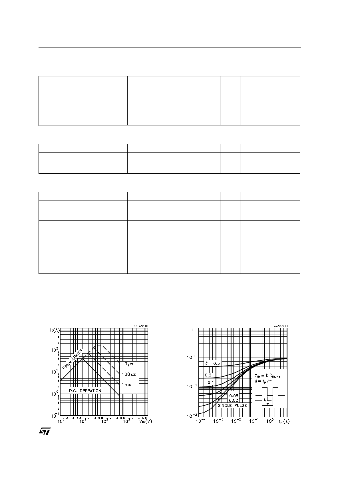
Safe Operating Area Thermal Impedance
3/8

STE38NB50
Output Characteris tics
Transconductance
Transfer Characteris tic s
Static Drain-source On Resist a nce
Gate Charge vs Gate-source Voltage
4/8
Capacitance Variations

STE38NB50
Normalized Gate Threshold Volt a ge vs
Temperature
Source-drain Diode Forward Characteris tic s
Normalized On Resistance vs Temperat ure
5/8

STE38NB50
Fig. 1: Unclamped Inductive Load Test Circuit
Fig. 3: Switching Tim es Test Circuits For
Resistive Load
Fig . 2 : Unclamped Induct ive W aveform
Fig. 4: Gate Charge test Circuit
Fig. 5: Test Circuit For Inductive Load Switching
And Diode Recovery Times
6/8

ISOTOP MECHANICAL DATA
STE38NB50
DIM.
MIN. TYP. MAX. MIN. TYP. MAX.
A 11.8 12.2 0.466 0.480
B 8.9 9.1 0.350 0.358
C 1.95 2.05 0.076 0.080
D 0.75 0.85 0.029 0.033
E 12.6 12.8 0.496 0.503
F 25.15 25.5 0.990 1.003
G 31.5 31.7 1.240 1.248
H4 0.157
J 4.1 4.3 0.161 0.169
K 14.9 15.1 0.586 0.594
L 30.1 30.3 1.185 1.193
M 37.8 38.2 1.488 1.503
N4 0.157
O 7.8 8.2 0.307 0.322
mm inch
N
O
G
A
B
D
E
F
H
J
C
K
L
M
7/8

STE38NB50
Information furnished is believed to be accurate and reliable. However, STMicroelectronics assumes no responsibility for the consequences
of use of such inform ation nor for any infringe ment o f patents or other rig hts o f third par ties which ma y resul t from i ts use. N o li cen se is
granted by implicatio n or otherwise under any patent or patent rights of STMicroelectronics. Specification mentioned in this publication are
subject to change without notice. This publication supersedes and replaces all information previously supplied. STMicroelectronics products
are not authorized for use as critical compo nents in life support devices or systems without express written approval of STMicroelectronics.
The ST logo is a trademark of STMicroelectronics
© 1998 STMicroelectro nics – Printed in Italy – All Rights Reserved
STMicroelectronics GROUP OF COMPANIES
Australia - Brazil - Canada - China - France - Germany - Italy - Japan - Korea - Malaysia - Malta - Morocco - The Netherlands -
Singapore - Spain - Sweden - Switzerland - Taiwan - Thailand - United Kingdom - U.S.A.
.
8/8
 Loading...