

查询STE250N06供应商
POWER MOS TRANSISTOR IN ISOTOP PACKAGE
STE250N06
N - CHANNEL ENHANCEMENT MODE
TYPE V
DSS
R
DS(on)
I
D
STE250N06 60 V < 0.004 Ω 250 A
■ HIGH CURRENT POWER MODULE
■ AVALANCHE RUGGED TECHNOLOGY
(SEE STH80N06 FOR RATING)
■ VERY LARGE SOA - LARGE PEAK POWER
CAPABILITY
■ EASY TO MOUNT
■ SAME CURRENT CAPABILITY FOR THE
TWO SOURCE TERMINALS
■ EXTREMELY LOW R
■ VERY LOW DRAIN TO CASE CAPACITANCE
■ VERY LOW INTERNAL PARASITIC
JUNCTION TO CASE
th
INDUCTANCE (TYPICALLY < 5 nH)
■ ISOLATED PACKAGE UL RECOGNIZED
(FILE No E81743)
INDUSTRIAL APPLICATIONS:
■ SMPS & UPS
■ MOTOR CONTROL
■ WELDING EQUIPMENT
■ OUTPUT STAGE FOR PWM, ULTRASONIC
CIRCUITS
4
3
1
2
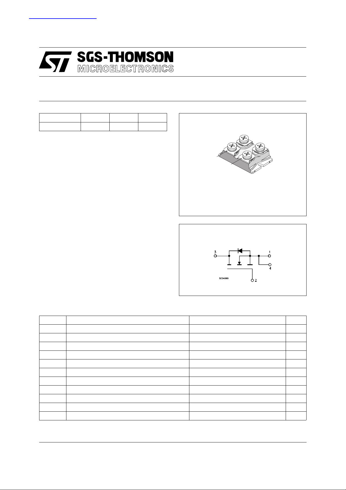
ISOTOP
INTERNAL SCHEMATIC DIAGRAM
ABSOLUTE MAXIMUM RATINGS
Symbol Parameter Value Unit
V
V
V
I
DM
P
T
V
(•) Pulse width limited by safe operating area
May 1995
Drai n -So ur ce Volt ag e ( VGS = 0) 60 V
DS
Drain-Gate Voltage (RGS = 20 kΩ)60V
DGR
Gate-Source Voltage ± 20 V
GS
I
Drain Current (continuous) at Tc = 25 oC250A
D
I
Drain Current (continuous) at Tc = 100 oC155A
D
(•) Drain Current (pulsed) 750 A
Total Dissipation at Tc = 25 oC450W
tot
Derating Factor 3.6 W/
Storage Temperature -55 to 150
stg
T
Max. Operating Junction Temperature 150
j
Insu lat ion With sta nd Volt age ( AC-RM S) 2500 V
ISO
o
C
o
C
o
C
1/8

STE250N06
THERMAL DATA
R
thj-case
R
thc-h
Thermal Resistance Junction-case Max
Thermal Resistance Case-heatsink With Conductive
Grease A p pl ied M ax
0.27
0.05
o
C/W
o
C/W
ELECTRICAL CHARACTERISTICS (T
= 25 oC unless otherwise specified)
case
OFF
Symbol Parameter Test Condition s Min. Ty p. Max. Unit
V
(BR) DSS
Drain-source
ID = 1 mA V
= 0 V 60 V
GS
Bre akdow n Vol tage
I
DSS
I
GSS
Zero Ga te V ol t ag e
Drain Current (V
GS
Gate -body Leaka ge
VDS = Max Rating
= 0)
VDS = Max Rating x 0.8 Tc = 125 oC
VGS = ± 20 V ± 400 nA
400
2
Current (VDS = 0)
ON (∗)
Symbol Parameter Test Condition s Min. Ty p. Max. Unit
V
R
GS(th)
DS(on)
Gate Threshold Voltage V
Stat ic Dra in-s ourc e On
= VGS ID = 1 mA 2 4 V
DS
VGS = 10V ID = 125 A 0.004 Ω
Resistance
DYNAMIC
Symbol Parameter Test Condition s Min. Ty p. Max. Unit
g
(∗)Forward
fs
Transconductance
C
C
C
Input Capacitance
iss
Output Capacitance
oss
Reverse Transfer
rss
Capacitance
VDS = 15 V ID = 125 A 100 S
V
= 25 V f = 1 MHz V
DS
= 0 V 25
GS
10000
3000
µA
mA
nF
pF
pF
SWITCHING ON
Symbol Parameter Test Condition s Min. Ty p. Max. Unit
(di/dt)
2/8
t
d(on)
Q
t
r
Turn-on Time
Rise Time
V
= 25 V ID = 125 A
DD
RG = 4.7 Ω VGS = 10 V
(see test circuit, figure 1)
Turn-on Current Slope VDD = 40 V ID = 250 A
on
RG = 4.7 Ω VGS = 10 V
(see test circuit, figure 3)
Tot al G a te C ha r ge VDD = 40 V ID = 250 A
g
VGS = 10 V
95
300
440 A/µs
475 nC
ns
ns

STE250N06
ELECTRICAL CHARACTERISTICS (continued)
SWITCHING OFF
Symbol Parameter Test Condition s Min. Ty p. Max. Unit
t
r(Voff)
t
SOURCE DRAIN DIODE
Symbol Parameter Test Condition s Min. Ty p. Max. Unit
I
SD
I
SDM
V
SD
t
Q
I
RRM
(∗) Pulsed: Pulse duration = 300 µs, duty cycle 1.5 %
(•) Pulse width limited by safe operating area
Off-voltage Rise Time
t
Fall Time
f
Cross-over Time
c
Source-drain Current
(•)
Source-drain Current
VDD = 40 V ID = 250 A
RG = 4.7 Ω VGS = 10 V
(see test circuit, figure 3)
140
745
1000
250
750
(pulsed)
(∗) F or w ar d On V ol t ag e ISD = 250 A VGS = 0 1.6 V
Reverse Recovery
rr
Time
Reverse Recovery
rr
ISD = 250 A di/dt = 100 A/µs
VDD = 25 V Tj = 150 oC
(see test circuit, figure 3)
210
1.31
Charge
Reverse Recovery
12.5
Current
ns
ns
ns
A
A
ns
µC
A
Safe Operating Area Thermal Impedance
3/8

STE250N06
Derating Curve
Transfer Characteristics
Output Characteristics
Transconductance
Static Drain-source On Resistance
4/8
Gate Charge vs Gate-source Voltage

STE250N06
Capacitance Variations Normalized Gate Threshold Voltage vs
Temperature
Normalized Breakdown Voltage vs Temperature Normalized On Resistance vs Temperature
Turn-off Drain-source Voltage SlopeTurn-on Current Slope
5/8

STE250N06
Cross-over Time Source-drain Diode Forward Characteristics
Fig. 1: Switching Times Test Circuits For
Resistive Load
Fig. 3: Test Circuit For Inductive Load Switching
And Diode Recovery Times
Fig. 2: Gate Charge Test Circuit
6/8

ISOTOP MECHANICAL DATA
STE250N06
DIM.
MIN. TYP. MAX. MIN. TYP. MAX.
A 11.8 12.2 0.466 0.480
B 8.9 9.1 0.350 0.358
C 1.95 2.05 0.076 0.080
D 0.75 0.85 0.029 0.033
E 12.6 12.8 0.496 0.503
F 25.15 25.5 0.990 1.003
G 31.5 31.7 1.240 1.248
H 4 0.157
J 4.1 4.3 0.161 0.169
K 14.9 15.1 0.586 0.594
L 30.1 30.3 1.185 1.193
M 37.8 38.2 1.488 1.503
N 4 0.157
O 7.8 8.2 0.307 0.322
P 5.5 0.216
mm inch
N
O
G
A
B
D
E
F
H
J
C
K
L
M
0041565
7/8

STE250N06
Information furn ished is belie ved to be acc urate and relia ble. However, SGS- THOMSON Micro electronics assu mes no respons ability for the
cons eq ue nce s o f u se o f such in fo rm ati o n nor f or a ny i nf rin ge me nt of pa te nt s or o th er ri gh ts o f thi rd pa r tie s w hic h ma y res ul t s fro m i t s us e. No
license is granted by implication or otherwise under any patent or patent rights of SGS-THOMSON Microelectronics. Specifications mentioned
in this publication are subject to change without notice. This publication supersedes and replaces all information previously supplied.
SGS-THOMSON Microelectronics products are not authori zed for use as critical components in life support devices or systems without express
written approval of SGS-THOMSON Microelectonics.
© 1997 SGS-THOMSON Microelectronics - Printed in Italy - All Rights Reserved
Australia - Brazil - Canada - China - France - Germany - Hong Kong - Italy - Japan - Korea - Malaysia - Malta - Morocco - The Netherlands -
Singapore - Spain - Sweden - Switzerland - Taiwan - Thailand - United Kingdom - U.S.A
SGS-THOMSON Microelectronics GROUP OF COMPANIES
.
8/8
 Loading...