

Page 1
查询STE2007DIE2供应商
STE2007
96 x 68 Single Chip LCD Controller/Driver
Features
■ 68 x 96 bits Display Data RAM
■ 33,49, 65 and 68 Lines Mode
■ Row by Row Scrolling
■ Interfaces
– 3-lines Serial Interface (read and write)
2
C (read and write)
–I
– 4-Line Serial (read and write)
■ Partial Display Mode (33,25,17,9 Lines Mode)
■ Fully Integrated Oscillator requires no external
components
■ CMOS Compatible Inputs
■ Programmable ID-Number
■ Programmable Bias Ratio
■ Programmable Columns Organization
■ Fully Integrated Configurable LCD bias voltage
generator with:
– Selectable multiplication factor (3x, 4X and
5X)
– Effective sensing for High Precision Output
– Eight selectable temperature compensation
coefficients
■ Designed for chip-on-glass (COG) applications
■ Low Power Consumption, suitable for battery
operated systems
■ Interfaces Supply Voltage range from 1.6 to
3.6V
■ High Voltage Generator Supply Voltage range
from 2.4 to 3.6V
■ Display Supply Voltage range from 3 to 13.2V
= 25°C)
(T
amb
Description
The STE2007 is a low power LCD driver, capable
to drive 96 columns and up to 68 lines, designed
for monochrome displays.
The STE2007 includes fully integrated bias
voltage generator (up to 5x multiplication factor),
and internal oscillator, thus reducing to minimum
the number of external components required and
the current consumption.
The STE2007 features the three standard serial
interfaces (3 and 4 lines serial, I
2
C interface).
Order codes
Type Ordering Number
Bumped Dice on Waffle Pack STE2007DIE2
Rev 1
November 2005 1/62
www.st.com
62
Page 2

STE2007
Contents
1 Introduction . . . . . . . . . . . . . . . . . . . . . . . . . . . . . . . . . . . . . . . . . . . . . . . . . . 5
2 Driver Pin Description . . . . . . . . . . . . . . . . . . . . . . . . . . . . . . . . . . . . . . . . . . 7
2.1 CPU Interface Pins . . . . . . . . . . . . . . . . . . . . . . . . . . . . . . . . . . . . . . . . . . . . . 7
2.2 Power Supply Pins . . . . . . . . . . . . . . . . . . . . . . . . . . . . . . . . . . . . . . . . . . . . . 7
2.3 Configuration Pins . . . . . . . . . . . . . . . . . . . . . . . . . . . . . . . . . . . . . . . . . . . . . . 8
2.4 Test Pins . . . . . . . . . . . . . . . . . . . . . . . . . . . . . . . . . . . . . . . . . . . . . . . . . . . . . 8
3 Display Driver Electrical Characteristics . . . . . . . . . . . . . . . . . . . . . . . . . 10
3.1 Absolute maximum ratings . . . . . . . . . . . . . . . . . . . . . . . . . . . . . . . . . . . . . . 10
3.2 DC Characteristics . . . . . . . . . . . . . . . . . . . . . . . . . . . . . . . . . . . . . . . . . . . . 11
3.3 AC Characteristics . . . . . . . . . . . . . . . . . . . . . . . . . . . . . . . . . . . . . . . . . . . . 12
3.4 MCU Tx Data Mode . . . . . . . . . . . . . . . . . . . . . . . . . . . . . . . . . . . . . . . . . . . 12
3.4.1 Driver TxData Mode . . . . . . . . . . . . . . . . . . . . . . . . . . . . . . . . . . . . . . . . . . . 13
3.4.2 Reset Timing . . . . . . . . . . . . . . . . . . . . . . . . . . . . . . . . . . . . . . . . . . . . . . . . . 14
4 INTERFACE . . . . . . . . . . . . . . . . . . . . . . . . . . . . . . . . . . . . . . . . . . . . . . . . . 16
4.1 3-lines 9 bit Serial Interface . . . . . . . . . . . . . . . . . . . . . . . . . . . . . . . . . . . . . 16
4.1.1 MCU TxData Mode (Write Mode) . . . . . . . . . . . . . . . . . . . . . . . . . . . . . . . . . 16
4.1.2 Driver TxData Mode (Read Mode) . . . . . . . . . . . . . . . . . . . . . . . . . . . . . . . . 17
4.2 4-Line SPI . . . . . . . . . . . . . . . . . . . . . . . . . . . . . . . . . . . . . . . . . . . . . . . . . . . 19
4.2.1 MCU TxData Mode (Write Mode) . . . . . . . . . . . . . . . . . . . . . . . . . . . . . . . . . 19
4.2.2 Driver TxData Mode (Read Mode) . . . . . . . . . . . . . . . . . . . . . . . . . . . . . . . . 21
4.3 I2C Bus . . . . . . . . . . . . . . . . . . . . . . . . . . . . . . . . . . . . . . . . . . . . . . . . . . . . . 21
4.3.1 Communication Protocol . . . . . . . . . . . . . . . . . . . . . . . . . . . . . . . . . . . . . . . . 23
4.3.2 Starting the Communication . . . . . . . . . . . . . . . . . . . . . . . . . . . . . . . . . . . . . 23
4.3.3 MCU TxData Mode (Write Mode) . . . . . . . . . . . . . . . . . . . . . . . . . . . . . . . . . 24
4.3.4 Driver TxData Mode (Read Mode) . . . . . . . . . . . . . . . . . . . . . . . . . . . . . . . . 25
4.4 Reading Mode . . . . . . . . . . . . . . . . . . . . . . . . . . . . . . . . . . . . . . . . . . . . . . . . 26
4.4.1 IIdentification byte . . . . . . . . . . . . . . . . . . . . . . . . . . . . . . . . . . . . . . . . . . . . . 26
5 Display Data RAM (DDRAM) . . . . . . . . . . . . . . . . . . . . . . . . . . . . . . . . . . . . 27
5.1 DDRAM and Page/column address circuit . . . . . . . . . . . . . . . . . . . . . . . . . . 27
2/62
Page 3

STE2007
5.2 Line address circuit . . . . . . . . . . . . . . . . . . . . . . . . . . . . . . . . . . . . . . . . . . . . 28
5.3 Partial Display . . . . . . . . . . . . . . . . . . . . . . . . . . . . . . . . . . . . . . . . . . . . . . . . 32
5.3.1 33 Line Partial Display Mode . . . . . . . . . . . . . . . . . . . . . . . . . . . . . . . . . . . . . 33
5.3.2 25 Line Partial Display Mode . . . . . . . . . . . . . . . . . . . . . . . . . . . . . . . . . . . . . 35
5.3.3 17 Line Partial Display Mode . . . . . . . . . . . . . . . . . . . . . . . . . . . . . . . . . . . . . 36
5.3.4 9 Line Partial Display Mode . . . . . . . . . . . . . . . . . . . . . . . . . . . . . . . . . . . . . . 37
5.4 Command Parameters Default Configuration . . . . . . . . . . . . . . . . . . . . . . . . 38
6 Instruction Setups . . . . . . . . . . . . . . . . . . . . . . . . . . . . . . . . . . . . . . . . . . . . 39
6.1 Initialization (Power ON Sequence) . . . . . . . . . . . . . . . . . . . . . . . . . . . . . . . 39
6.2 Display Data Writing Sequence . . . . . . . . . . . . . . . . . . . . . . . . . . . . . . . . . . 39
6.3 Power OFF . . . . . . . . . . . . . . . . . . . . . . . . . . . . . . . . . . . . . . . . . . . . . . . . . . 39
7 Power ON/Power OFF timing Sequence . . . . . . . . . . . . . . . . . . . . . . . . . . 40
8 Commands . . . . . . . . . . . . . . . . . . . . . . . . . . . . . . . . . . . . . . . . . . . . . . . . . . 43
8.1 Display ON/OFF . . . . . . . . . . . . . . . . . . . . . . . . . . . . . . . . . . . . . . . . . . . . . . 43
8.2 Display normal/reverse . . . . . . . . . . . . . . . . . . . . . . . . . . . . . . . . . . . . . . . . . 43
8.3 Display all points ON/OFF . . . . . . . . . . . . . . . . . . . . . . . . . . . . . . . . . . . . . . 43
8.4 Page address set . . . . . . . . . . . . . . . . . . . . . . . . . . . . . . . . . . . . . . . . . . . . . 44
8.5 Column address set . . . . . . . . . . . . . . . . . . . . . . . . . . . . . . . . . . . . . . . . . . . 44
8.6 Display start line address set . . . . . . . . . . . . . . . . . . . . . . . . . . . . . . . . . . . . 45
8.7 Segment driver direction select . . . . . . . . . . . . . . . . . . . . . . . . . . . . . . . . . . . 45
8.8 Common driver direction select . . . . . . . . . . . . . . . . . . . . . . . . . . . . . . . . . . 45
8.9 Display data write . . . . . . . . . . . . . . . . . . . . . . . . . . . . . . . . . . . . . . . . . . . . . 46
8.10 Data reading from driver (Driver TxData–mode) . . . . . . . . . . . . . . . . . . . . . . 46
8.11 Power Control Set . . . . . . . . . . . . . . . . . . . . . . . . . . . . . . . . . . . . . . . . . . . . . 46
8.12 VLCD set . . . . . . . . . . . . . . . . . . . . . . . . . . . . . . . . . . . . . . . . . . . . . . . . . . . . 47
8.12.1 V0R - Voltage Range Set . . . . . . . . . . . . . . . . . . . . . . . . . . . . . . . . . . . . . . . 47
8.12.2 VOP Set . . . . . . . . . . . . . . . . . . . . . . . . . . . . . . . . . . . . . . . . . . . . . . . . . . . . . 48
8.12.3 Electronic volume . . . . . . . . . . . . . . . . . . . . . . . . . . . . . . . . . . . . . . . . . . . . . 49
8.13 Power saver mode . . . . . . . . . . . . . . . . . . . . . . . . . . . . . . . . . . . . . . . . . . . . 49
8.14 Reset . . . . . . . . . . . . . . . . . . . . . . . . . . . . . . . . . . . . . . . . . . . . . . . . . . . . . . . 50
8.15 NOP . . . . . . . . . . . . . . . . . . . . . . . . . . . . . . . . . . . . . . . . . . . . . . . . . . . . . . . 50
8.16 Image Location . . . . . . . . . . . . . . . . . . . . . . . . . . . . . . . . . . . . . . . . . . . . . . . 50
3/62
Page 4

STE2007
8.17 Bias Ratio . . . . . . . . . . . . . . . . . . . . . . . . . . . . . . . . . . . . . . . . . . . . . . . . . . . 51
8.18 Temperature Compensation . . . . . . . . . . . . . . . . . . . . . . . . . . . . . . . . . . . . . 52
8.19 Charge Pump Multiplication Factor . . . . . . . . . . . . . . . . . . . . . . . . . . . . . . . . 52
8.20 Refresh Rate . . . . . . . . . . . . . . . . . . . . . . . . . . . . . . . . . . . . . . . . . . . . . . . . . 53
8.21 Icon Mode . . . . . . . . . . . . . . . . . . . . . . . . . . . . . . . . . . . . . . . . . . . . . . . . . . . 53
8.22 N- Line Inversion . . . . . . . . . . . . . . . . . . . . . . . . . . . . . . . . . . . . . . . . . . . . . . 53
8.23 Number of Lines . . . . . . . . . . . . . . . . . . . . . . . . . . . . . . . . . . . . . . . . . . . . . . 54
9 Chip Mechanical Drawing . . . . . . . . . . . . . . . . . . . . . . . . . . . . . . . . . . . . . . 55
10 Revision history . . . . . . . . . . . . . . . . . . . . . . . . . . . . . . . . . . . . . . . . . . . . . . 61
4/62
Page 5

STE2007 1 Introduction
1 Introduction
In this document is specified LCD driver for Black&White full graphic displays with a resolution
of 96x68, 96x65, 96x49, and 96x33 (ColumnsXRows).
Abbreviations
LCD Liquid Crystal Display
COG Chip On Glass –technology
MCU Micro Controller Unit
DDRAM Display Data Random Access Memory
MSB Most Significant Bit
LSB Least Significant Bit
T.B.D. To Be Defined
Table 1. General Driver Parameters
Driver assembly technology
Chip On Glass (COG)
Memory Size
(Columns x Rows)
96x68
DDRAM capacity:
6528 bits
Mux
1:68
1:65
1:49
1:33
Frame frequency (Hz)
65
70
75
80
5/62
Page 6

1 Introduction STE2007
Figure 1. Chip Mechanical Drawing
R66
STE2007
45µm
(0,0)
X
BUMP SIDE
Y
72µm
! /
!
!
VSS_AUX
VSS_AUX
VSS_AUX
VSS_AUX
R67
R65
6/62
Page 7

STE2007 2 Driver Pin Description
2 Driver Pin Description
2.1 CPU Interface Pins
Table 2. CPU Interface Logic
PIN Signal Type Description Note
!RES I Reset Input
When Low the
!CS I Chip Select Input
SDOUT 0 Serial Data Output
SDAIN I
SCLK I
SDA_OUT 0
SA1 I
SA0 I
!D/C I 4 Line SPI Data/Command Selector
Serial Data Input /I
Serial Clock Input/I
2
C Bus Data Out
I
2
C Slave Address
I
2
C Slave Address
I
2
C Interface Data Input
2
C Interface Clock
communication port is
enabled
Must be connected to
SDAIN at Module
Level
Must be left floating
when I2C Interface is
not is use
Cannot be left floating
Cannot be left floating
Must be connected to
VSSAUX at Module
Level when 4-Line SPI
is not in USE
2.2 Power Supply Pins
Table 3. Power Supply Pins
PIN Signal Type Description Note
VSS Power Analog & Digital Grounds
VSS_LCD Power Drivers Analog Ground
VSS_CP Power Booster Ground
VDDI Power Digital Power
VDD Power Analog Supply
VDD_CP Power Booster Power Supply
VSSAUX Power Auxiliar Vss Output
Table 4. High Voltage Pins
PIN Signal Type Description Note
V
LCD
V
LCD_SENSE
High
Voltage
High
Voltage
Booster Output
Booster Sense Input
Cext = 0.1-1µF
Connected to Vss
Must be connected to
Vlcd at module level
7/62
Page 8

2 Driver Pin Description STE2007
Table 4. High Voltage Pins (continued)
PIN Signal Type Description Note
COM0 to
COM67
COMS
SEG0 to
SEG95
High
Voltage
High
Voltage
High
Voltage
2.3 Configuration Pins
Table 5. Configuration Pin Description
PIN Signal Type Config Description Note
OSCIN I
SEL0 -SEL1 I
LCD Row Driver Output
LCD Row Driver Output
LCD Column Driver Output
VSS/VSSAUX Internal Oscillator Stopped
VDDI Internal Oscillator Active
SEL1 SEL0 Interface
VSS/VSSAUX VSS//VSSAUX
VSS/VSSAUX VDD1 SPI 4-Lines 8 bit
VDD1 VSS/VSSAUX Serial 3-Lines 9 bit
VDD1 VDD1 Not Used
Unused lines must be
left floating
Unused lines must be
left floating
Unused lines must be
left floating
2
C
I
2.4 Test Pins
Table 6. Test Pin Description
PIN Signal Type Description Note
T2 I Test Input. Enable Test Mode.
T1 I Test Input. Enable Test Mode.
T0 I Test Input.
T3 O Test Output.
IDA I
VSS/VSSAUX IDA=”0”
VDDI IDA=”1”
VSS/VSSAUX IDB=”0”
IDB I
VDDI IDB=”1”
Must Be connected to VSS
in Normal Working Mode
Must Be connected to VSS
in Normal Working Mode
Must Be connected to VSS
in Normal Working Mode
Must Be OPEN in Normal
Working Mode
8/62
Page 9
STE2007 2 Driver Pin Description
Table 6. Test Pin Description (continued)
PIN Signal Type Description Note
T4 O Test Output.
T5 O Test Output.
T6 O Test Output.
VREF_B
UFF
O Analog Test Output Must be left floating
Must Be OPEN in Normal
Working Mode
Must Be OPEN in Normal
Working Mode
Must Be OPEN in Normal
Working Mode
9/62
Page 10
3 Display Driver Electrical Characteristics STE2007
3 Display Driver Electrical Characteristics
3.1 Absolute maximum ratings
Table 7. Absolute maximum ratings
Symbol Parameter Value Unit
V
DDI
V
DD
V
LCD
I
SS
V
I
in
I
out
P
tot
P
o
T
T
stg
All pins vs
VDDI (*) ESD Maximum Withstanding Voltage Range
All other
pins / pin
Supply Voltage Range - 0.5 to + 5 V
Supply Voltage Range - 0.5 to + 5 V
LCD Supply Voltage Range - 0.5 to + 14.0 V
Supply Current - 50 to +50 mA
Digital Inputs Voltage
i
-0.5 to V
DDI
DC Input Current - 10 to + 10 mA
DC Output Current - 10 to + 10 mA
Total Power Dissipation (Tj = 85°C)
300 mW
Power Dissipation per Output 30 mW
Operating Junction Temperature -40 to + 85 °C
j
Storage Temperature - 65 to 150 °C
±1750 V
Test Condition: CDF-AEC-Q100-002- “Human Body Model”
Acceptance Criteria: “Normal Performance”
±2000 V
+ 0.5
combination
Note: (*) ESD tests have been performed with VSS, VSS_LCD and VSS_CP shorted together
V
10/62
Page 11
STE2007 3 Display Driver Electrical Characteristics
3.2 DC Characteristics
Table 8. DC characteristics
Symbol Parameter Test Condition Min. Typ. Max. Unit
V
DD,VDDCP
V
DDI
V
LCD
V
LCD_SENSE
V
LCD
I(V
)
DDI
I(VDD+V
DDCP
)
Logic Inputs
V
IH
V
IL
I
IH
I
lL
Logic Outputs
V
OH
V
OL
Power Supply Voltage Operating Voltage 2.4 3.6 V
Power Supply Voltage(Logic) I/O supply Voltage 1.6 3.6 V
Booster Output 13.5 V
Booster Sense Input 13.5 V
LCD Supply Voltage Accuracy
Logic Supply Current
LCD=10V; VDD=2.6V; T
V
25°C; No display Load;
f
=0Hz
SCLK
Power Saver Mode ON
(Interfaces quiescent)
Power Saver Mode OFF
(Interfaces quiescent)
amb
=
-2 2 %
13µA
620µA
Write Mode 120 250 µA
=10V;Booster= 5X;
V
LCD
f
=0Hz; VDD=2.4V
Analog Supply Current
Logic High level input voltage
Logic Low level input voltage Vss
SCLK
Refresh Rate=75Hz;
no display load;T
amb
= 25°C
0.7V
90 180 µA
DD
I
V
0.3V
DDI
I
DD
V
V
Logic High level input current 1 µA
Logic Low level input current -1 µA
0.8V
Logic High level output voltage
Logic Low level output voltage
= -500µA; VDDI=1.6V
l
OUT
= 500µA; VDDI=1.6V
l
OUT
I
Vss
DD
V
0.2V
DDI
DDl
V
V
Note: 1 T
= -40 to 85°C, unless otherwise specified.
amb
11/62
Page 12

3 Display Driver Electrical Characteristics STE2007
3.3 AC Characteristics
Table 9. AC Operation - Internal Oscillator
Symbol Parameter Test Condition Min. Typ. Max. Unit
VDDI= 1.6; VDD= 2.9V
F
FRAME
Frame Frequency Default
Rafresh Rate = 75Hz
Tamb = -20°C to +70°C
68 75 82 Hz
3.4 MCU Tx Data Mode
Table 10. AC Characteristics for Serial interface
Description Signal Symbol Notes Min. Typ. Max. Unit
tcss 60 ns
Chip Select !CS
Input Serial Data Interface SDAIN
Output Serial Data interface SDAOUT
Serial clock input SCLK
tcsh 100 ns
tchw 50 ns
tsds Data setup time 100 ns
tsdh Data hold time 100 125 ns
tac Access Time 0 100 ns
tod
Output Disable
Time
25 100 ns
tscyc Serial clock cycle 250 ns
tshw
tslw
Serial clock H
pulse width
Serial clock L
pulse width
100 ns
100 ns
Note: 1 The input signal rise and fall times must be within 10ns.
2 Every timing is specified on the basis of 30% and 70% of VDDI.
3T
= -40 to 85°C, unless otherwise specified.
amb
Figure 2. MCU TxData timing
tchw
!CS
SCLK
tf
SDA/MCU TxData
tcss tcsh
tslw
tscyc
tr
tsdhtsds
tchw
tshw
12/62
Page 13

STE2007 3 Display Driver Electrical Characteristics
Table 11. Input Signals Change Time
Signal Symbol Parameter Minimum
Inputs tr,tf 10 ns / to 30% & 70% levels
Typical/
Nominal
Maximum Unit / Notes
3.4.1 Driver TxData Mode
Table 12. Timings based on 4 MHz SCLK Speed
Item Symbol Condition Rating Units
Min. Max.
Data hold time T1 Note 1 100 125 ns
Access time T2 – 10 100 ns
Output disable time T3 – 25 100 ns
Data setup time T4 – 100 – ns
!CS pulse width high T5 – 250 ns
Note: 1 Data Hold Time T1 depends on SCLK high time and Max Data Hold time. It is Always 3-8ns
before SCLK pulse falling edge
2 The input signal rise and fall times must be within 10ns.
3 Every timing is specified on the basis of 30% and 70% of VDDI.
4T
= -40 to 85°C, unless otherwise specified.
amb
Table 13. Timings based on 1 MHz SCLK Speed
Item Symbol Condition Rating Units
Min. Max.
Data hold time *) T1 – 100 125 ns
Access time T2 – 10 450 ns
Output disable time T3 – 25 450 ns
Data setup time T4 – 100 – ns
1CS pulse width high T5 – 250 ns
Note: 1 The input signal rise and fall times must be within 10ns.
2 Every timing is specified on the basis of 30% and 70% of VDDI.
3T
= -40 to 85°C, unless otherwise specified.
amb
13/62
Page 14
3 Display Driver Electrical Characteristics STE2007
Figure 3. Driver TxData Mode AC timing characteristics
Timing BTiming A
SCLK
MCU TxData
MCU Data direction
Driver TxData
Timing A
SCLK
MCU TxData
Driver TxData
Driver SDA direction
!CS
Timing B
SCLK
MCU TxData
Command
Tx TxRx
Hi±Z
Hi±Z Status
in out
Hi±Z
T1 T2
T3 T4
Command
Hi±Z
D/C
Driver TxData
out inDriver SDA direction
T5
!CS
1/2 SCLK
1/2 SCLK
3.4.2 Reset Timing
Table 14. Reset Timing
Description Signal Symbol Min. Max. Unit
Reset time !RES trs 2500
Reset rejection (for noise spike) !RES trj 1000
Note: 1 The input signal rise and fall times must be within 10ns.
2 Every timing is specified on the basis of 30% and 70% of VDDI.
3T
= -40 to 85°C, unless otherwise specified.
amb
nsReset low pulse width (for valid reset) !RES trw 2500
14/62
Page 15

STE2007 3 Display Driver Electrical Characteristics
Figure 4.
!RES
Internal circuit status
trj
trw
During reset
trs
Normal operation
15/62
Page 16

4 INTERFACE STE2007
4 INTERFACE
4.1 3-lines 9 bit Serial Interface
STE2007 3-lines 9 bits serial interface is a bidirectional link between the display driver and the
host processor.
It consists of three lines:
– SDAIN/SDAOUT Serial Data
– SCLK Serial Clock
– !CS Peripheral enable: - Active Low- Enables and Disables the serial interface
The serial interface is active only if the !CS line is low. If !CS is low after the positive edge of
!RES, the serial interface is ready to receive data after the internal reset time. Serial data must
be input to SDA in the sequence D/!C, D7 to D0. STE2007 read data on SCLK rising edge. The
first bit of serial data D/!C is data/command flag. When D/!C =”1” D7 to D0 bits are display RAM
data or Command Parameters. When D/!C=”0” D7 to D0 bits identify a command
4.1.1 MCU TxData Mode (Write Mode)
STE2007 is always a slave device on the communication bus and receive the communication
clock on the SCLK pin from the master. Information are exchanged word-wide. Every word is
composed by 9 bit. The first bit is named D/!C and indicates whether the following byte is a
command (D/!C =0) or a Display Data Byte (D/!C =1).
During data transfer, the data line is sampled by the receiver unit on the SCLK rising edge.
The data/command received is transferred to DDRAM or Executed on the first falling edge after
the latching rising edge or on the !CS rising edge.
If !CS stays low after the last bit of a command/data byte, the serial interface expects the D/!C
bit of the next data byte on the next SCLK positive edge.
A reset pulse on !RES pin interrupts any transmission.
Figure 5.
!CS
SDA
SCLK
D/C D7 D6 D5 D4 D3 D2 D1 D0 D/C
123456789
4.1.1.1 Data/Command Transfer break
If the Host processor generates an break condition (!CS Line HIGH before having received Bit
D0) while transferring a Data byte to the Frame Memory or a Command identifier or a command
parameter, the not complete received byte is discarded, the communication is interrupted and
the interface is forced in reset state.
D7 D6 D5 D4
1110 12 13 14
When !CS line becomes low again to start a new communication session STE2007 is ready to
receive the same byte interrupted re-transmitted or a new command identifier.
16/62
Page 17

STE2007 4 INTERFACE
3
Figure 6. 3-lines SPI Data Transfer break condition
Break
!CS
SCL
SDA
D7 D6 D5 D4 D3 D7 D6 D5 D4
COMMAND/PARAMETER COMMAND/PARAMETER
4.1.1.2 Data/Command Transfer pause
It is possible while transferring Frame Memory Data, Commands or Command Parameters to
insert a pause in the data transmission (!CS Line HIGH after 8 Bits Received). When !CS is
forced high after a whole byte received, the received byte is processed. Then STE2007 is
forced in a wait state ready to restart processing incoming data from the point where the
communication has been paused
If a new command identifier is transferred after a pause condition the previous communication
session is definitively closed.
Four are the possible conditions:
– Command-Pause-Command
– Command-Pause-Parameter
– Parameter-Pause-Command
– Parameter-Pause-Parameter
D/!C
LR0204
Figure 7. 3-lines SPI Data Transfer Pause
Pause
!CS
SCL
SDA
D3 D2 D1 D0 D7 D6 D5 D4 D3
COMMAND/PARAMETER COMMAND/PARAMETER
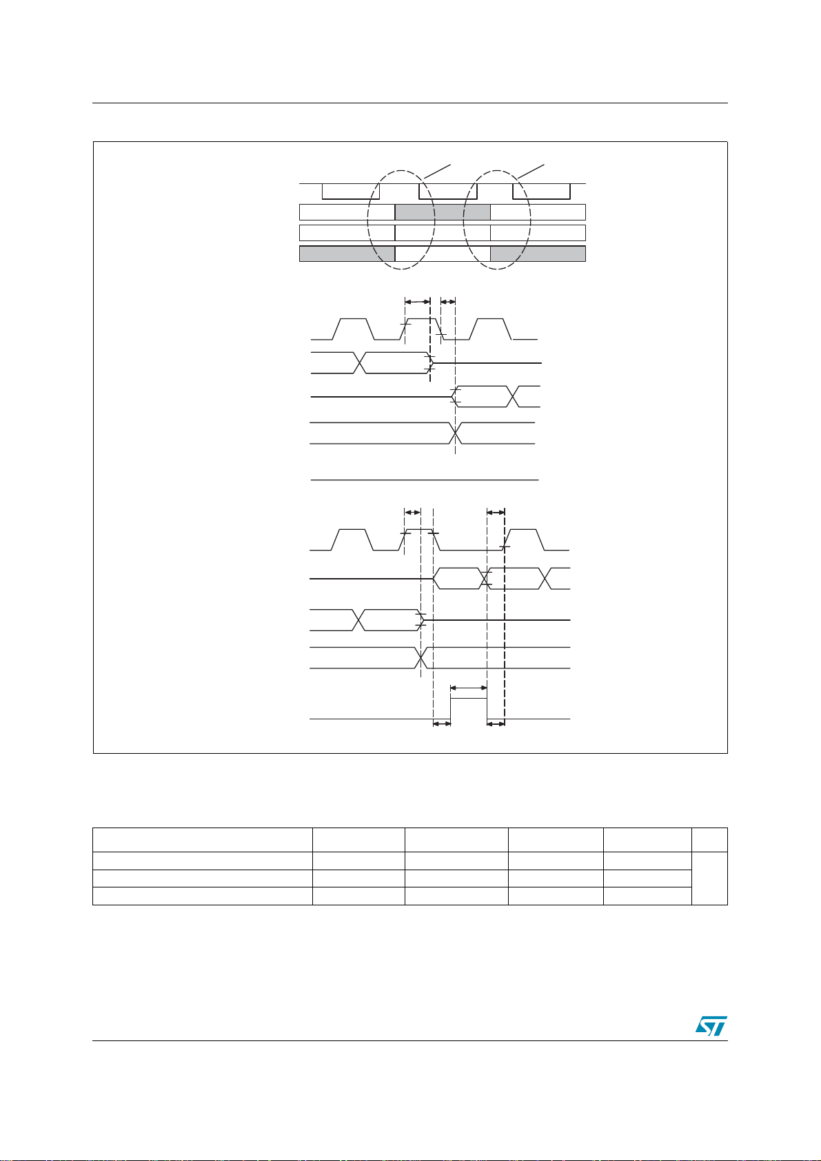
4.1.2 Driver TxData Mode (Read Mode)
The Driver TxData–mode is a method to check the electrical interconnection between LCD
driver and baseband, to identify the driver and for VDD Intercfonnection electrical self testing.
D/!C
D2 D1 D0
LR020
17/62
Page 18

4 INTERFACE STE2007
Self Testing of the electrical contacts is based on the monitoring of VLCD. The improper
electrical contact on VDD can be noted from a too low level of VLCD.
The serial interface Driver TxData–mode is controlled by three input signals.
The serial data output (SDAOUT/Driver TxData) and serial clock input (SCLK) are enabled
when !CS is low after having received one Reading Command.
To access Driver TxData–mode a Reading command must be sent to STE2007 driver. The first
bit (D/C) is low to indicates next 8–bits are for command. The data is read to the driver on the
rising edge of SCLK (see section ”MCU TxData–mode”). After last command bit (bit 0) is read
SDAOUT becomes active (Low impedance) and MCU is able to read data from driver.
SDAOUT is forced in high impedence when !CS line is forced high or after the eight SCLK rising
edges from the last SCLK rising edge of teh reading command transfer (Figure 8).
After sending out all 8 bits the driver release automatically the bus and go back to the MCU
TxData–mode. MCU Txdata line changes from high–z to active low or high in the falling edge of
8th SCLK pulse. !CS must be set high and low again before !D/C writing can continue.
If !CS is forced high during the Driver TxDAta-mode, the Driver Tx data session is aborted and
SDAOUT is forced in high impedance Mode.
SDAOUT and SDAIN line can be short circuited in normal working conditions.
Figure 8. AC timing characteristics
Timing BTiming A
SCLK
MCU TxData
MCU Data direction
Driver TxData
Command
Tx TxRx
Hi±Z
Hi±Z Status
Hi±Z
Command
Hi±Z
Timing A
SCLK
MCU TxData
Driver TxData
Driver SDA direction
!CS
Timing B
SCLK
MCU TxData
Driver TxData
!CS
T1 T2
in out
T3 T4
out inDriver SDA direction
1/2 SCLK
D/C
T5
1/2 SCLK
18/62
Page 19

STE2007 4 INTERFACE
Figure 9. Timing chart for start and stop of data reading from driver
Self Test command writing Reading of status D/C writing
SCLK
MCU TxData
0
Driver TxData
!CS
MCU TxData begins
1
D/C='0' 7
4.2 4-Line SPI
STE2007 4-lines serial interface is a bidirectional link between the display driver and the host
processor.
It consists of four lines:
– SDA Serial Data
– SCL Serial Clock
– !CS Peripheral enable: - Active Low- Enables and Disables the serial interface
– Mode selection (D/!C).
28912
...
...
High Z
...
1
0
Driver TxData begins
7
...
High Z
...
...
6
...
8
7
0
1
MCU TxData begins
1
2
D/C
7
The serial interface is active only if the !CS line is low. If !CS is low after the positive edge of
!RES, the serial interface is ready to receive data after the internal reset time.
4.2.1 MCU TxData Mode (Write Mode)
STE2007 is always a slave device on the communication bus and receive the communication
clock on the SCL pin from the master. Information are exchanged byte-wide. During data
transfer, the data line is sampled by the receiver unit on the SCL rising edge.
D/!C line status set whether the byte is a command (D/!C =0) or a data (D/!C =1); D/!C line is
read on the eighth SCL clock pulse during every byte transfer.
If !CS stays low after the last bit of a command/data byte, the serial interface expects the MSB
of the next data byte on the next SCL positive edge.
If !CS line is forced high in the middle of a data transfer, not complete Data bytes and
Commands bytes are discarded.
A reset pulse on !RES pin interrupts any transmission.
19/62
Page 20
4 INTERFACE STE2007
9
0
Figure 10. 4-lines SPI Commands Transfe
!CS
D/!C
SCL
SDA
(input)
SDA
(output)
D7 D6 D5 D4 D3 D2 D1 D0 D7 D6 D5 D4 D3 D2 D1 D0 D7
Hi-Z
COMMAND COMMAND
D6 D5 D4 D3 D2 D1 D0 D7 D6
COMMAND COMMAND
D0 D7 D6 D5 D4 D3 D2 D1 D0
LR018
Figure 11. 4-lines SPI Video Data Write Cycle
!CS
D/!C
SCL
SDA
(input)
SDA
(output)
D7 D6 D5 D4 D3 D2 D1 D0 D7 D6 D5 D4 D3 D2 D1 D0 D7
Hi-Z
COMMAND
DATA to VIDEO RAM
D6 D5 D4 D3 D2 D1 D0 D7 D6
DATA to VIDEO RAM
D0 D7 D6 D5 D4 D3 D2 D1 D0
DATA to VIDEO RAM
LR019
4.2.1.1 Data/Command Transfer break
If the Host processor generates an break condition (!CS Line HIGH before having received Bit
D0) while transferring a Data byte to the Frame Memory or a Command identifier or a command
parameter, the not complete received byte is discarded, the communication is interrupted and
the interface is forced in reset state.
When !CS line becomes low again to start a new communication session STE2007 is ready to
receive the same byte interrupted re-transmitted or a new command identifier.
Figure 12. 4-lines SPI Data Transfer break condition
!CS
D/!C
SCL
SDA
D7 D6 D5 D4 D3 D7 D6 D5 D4 D3
COMMAND/PARAMETER COMMAND/PARAMETER
4.2.1.2 Data/Command Transfer pause
Break
LR0192
It is possible while transferring Frame Memory Data, Commands or Command Parameters to
insert a pause in the data transmission (!CS Line HIGH after 8 Bits Received). When !CS is
forced high after a whole byte received, the received byte is processed. Then STE2007 is
forced in a wait state ready to restart processing incoming data from the point where the
communication has been paused
20/62
Page 21
STE2007 4 INTERFACE
5
If a new command identifier is transferred after a pause condition the previous communication
session is definitively closed.
Four are the possible conditions:
– Command-Pause-Command
– Command-Pause-Parameter
– Parameter-Pause-Command
– Parameter-Pause-Parameter
Figure 13. 4-lines SPI Data Transfer Pause
Pause
!CS
D/!C
SCL
SDA
D3 D2 D1 D0 D7 D6 D5 D4 D3
COMMAND/PARAMETER COMMAND/PARAMETER
4.2.2 Driver TxData Mode (Read Mode)
Throughout SDA line is possible to read some registers value (ID Numbers, Status byte,
temperature).
SDA (output Driver) is in High impedance in steady state and during data write.
Figure 14. 4-lines SPI 8Bit Read Cycle
DATA
High Z
!CS
D!C
SCL
SDA
(Input)
SDA
(Output)
MCU Data Tx Start
Read Command
D7 D6 D5 D4 D3 D2 D1 D0
High Z
LCD Driver Data Tx Start
D7 D6 D5 D4 D3 D2 D1
D2 D1 D0
LR0191
Next Command
D7 D6 D5 D4 D3 D2 D1 D0
D0
LR025
MCU Data Tx Start
4.3 I2C Bus
The I2C interface is a fully complying I2C bus specification, selectable to work in both Fast
(400kHz Clock) and High Speed Mode (3.4MHz).
This bus is intended for communication between different ICs. It consists of two lines: one bidirectional for data signals (SDA) and one for clock signals (SCL). Both the SDA and SCL lines
must be connected to a positive supply voltage via an active or passive pull-up.
The following protocol has been defined:
21/62
Page 22

4 INTERFACE STE2007
– Data transfer may be initiated only when the bus is not busy.
– During data transfer, the data line must remain stable whenever the clock line is high.
Changes in the data line while the clock line is high will be interpreted as a Start or
Stop Data Transfer condition (see below).
Accordingly, the following bus conditions have been defined:
BUS not busy: Both data and clock lines remain High.
Start Data Transfer: A change in the state of the data line, from High to Low, while the clock is
High, define the START condition.
Stop Data Transfer: A Change in the state of the data line, from low to High, while the clock
signal is High, defines the STOP condition.
Data Valid: The state of the data line represents valid data when after a start condition, the
data line is stable for the duration of the High period of the clock signal. The data on the line
may be changed during the Low period of the clock signal. There is one clock pulse per bit of
data.
Each data transfer starts with a start condition and terminated with a stop condition. The
number of data bytes transferred between the start and the stop conditions is not limited. The
information is transmitted byte-wide and each receiver acknowledges with the ninth bit.
By definition, a device that gives out a message is called "transmitter", the receiving device that
gets the signals is called "receiver". The device that controls the message is called "master".
The devices that are controlled by the master are called "slaves"
Acknowledge. Each byte of eight bits is followed by one acknowledge bit. This acknowledge
bit is a low level put on the bus by the receiver, whereas the master generates an extra
acknowledge related clock pulse.
A slave receiver which is addressed must generate an acknowledge after the reception of each
byte. Also, a master receiver must generate an acknowledge after the reception of each byte
that has been clocked out of the slave transmitter. The device that acknowledges has to pull
down the SDA_IN line during the acknowledge clock pulse. Of course, setup and hold time
must be taken into account. A master receiver must signal an end-of-data to the slave
transmitter by not generating an acknowledge on the last byte that has been clocked out of the
slave. In this case, the transmitter must leave the data line High to enable the master to
generate the STOP condition.
Connecting SDA_IN and SDA_OUT together the SDA line become the standard data line.
Having the acknowledge output (SDAOUT) separated from the serial data line is advantageous
in Chip-On-Glass (COG) applications. In COG applications where the track resistance from the
SDAOUT pad to the system SDA line can be significant, a potential divider is generated by the
bus pull-up resistor and the Indium Tin Oxide (ITO) track resistance. It is possible that during
the acknowledge cycle the STE2007 will not be able to create a valid logic 0 level. By splitting
the SDA input from the output the device could be used in a mode that ignores the
acknowledge bit. In COG applications where the acknowledge cycle is required, it is necessary
to minimize the track resistance from the SDACK pad to the system SDA line to guarantee a
valid LOW level.
2
To be compliant with the I
C-bus Hs-mode specification the STE2007 is able to detect the
special sequence "S00001xxx". After this sequence no acknowledge pulse is generated.
Since no internal modification are applied to work in Hs-mode, the device is able to work in Hsmode without detecting the master code.
22/62
Page 23

STE2007 4 INTERFACE
Figure 15. Bit transfer and START,STOP conditions definition
DATA LINE
STABLE
DATA VALID
CLOCK
DATA
START
CONDITION
Figure 16. Acknowledgment on the I
START
SCLK FROM
MASTER
DATA OUTPUT
BY TRANSMITTER
DATA OUTPUT
BY RECEIVER
1
MSB LSB
4.3.1 Communication Protocol
The STE2007 is an I2C slave. The access to the device is bi-directional since data write and
status read are allowed.
Four are the device addresses available for the device. All have in common the first 5 bits
(01111). The two least significant bit of the slave address are set by connecting the SA0 and
SA1 inputs to a logic 0 or to a logic 1.
CHANGE OF
DATA ALLOWED
2
C-bus
289
D00IN1151
D00IN1152
STOP
CONDITION
CLOCK PULSE FOR
ACKNOWLEDGEMENT
4.3.2 Starting the Communication
To start the communication between the bus master and the slave LCD driver, the master must
initiate a START condition. Following this, the master sends an 8-bit byte, on the SDA bus line
(Most significant bit first). This consists of the 7-bit Device Address Code, and the 1-bit Read/
Write Designator (R/W
communication (read or write).
All slaves with the corresponding address acknowledge in parallel, all the others will ignore the
2
I
C-bus transfer.
). The R/W bit has to be set to logic 1 to logic 0 according to the type of
ADDRESS BYTE
STE2007
SLAVE ADDRESS
S
011110AR/
S
A
W
1
READ or WRITE
DESIGNATOR
23/62
Page 24

4 INTERFACE STE2007
4.3.3 MCU TxData Mode (Write Mode)
If the R/W bit is set to logic 0 the STE2007 is set to be a receiver and the master can send
commands or data.
After the communication has started and slaves have acknowledged, the master sends a
control byte defined as follows and waits for its acknowledgement:
CONTROL BYTE
Co
DC
000
000
The Co bit is the control byte MSB and defines if after this control byte will follow a single byte
sequence (Co = 1) or a multiple bytes sequence (Co = 0). The D/C
following byte (if Co = 1) or the following stream of bytes (if Co = 0) are command (D/C
DDRAM data (D/C
= 1).
bit defines whether the
= 0) or
Depending on state of flags Co and D/C, four writing sequences are possible:
SINGLE COMMAND BYTE SEQUENCE (Co = 1, D/C
= 0): a single byte interpreted as a
command will follow the control byte;
SINGLE DATA BYTE SEQUENCE (Co = 1, D/C
= 1): a single byte interpreted as a data to be
written in DDRAM will follow the control byte;
MULTIPLE COMMAND BYTES SEQUENCE (Co = 0, D/C
= 0): a stream of bytes will follow the
control byte, with each single byte interpreted as a command;
MULTIPLE DATA BYTES SEQUENCE (Co = 0, D/C
= 1): a stream of bytes will follow the
control byte, with each byte interpreted as a data byte to be written in DDRAM.
Every single byte of a sequence must be acknowledged by all addressed units.
A multiple data sequence is terminated only by sending a STOP condition on the I
When a sequence is terminated, another sequence of any type can follow or a I
2
C bus.
2
C STOP
condition can be sent to close the communication.
In a single or multiple data bytes sequence, every data byte received is stored in the DDRAM at
the location specified by the current values of data pointers. Data pointers are automatically
updated after each single data byte written.
24/62
Page 25

STE2007 4 INTERFACE
4.3.4 Driver TxData Mode (Read Mode)
If the R/W bit is set to logic 1 the chip will output data immediately after the slave address. If the
D/C bit during the last write access, is set to a logic 0, the byte read is the status byte.
Figure 17. Communication Protocol
WRITE MODE
COMMUNICATION
START
SINGLE COMMAND
SEQUENCE
MULTIPLE COMMAND
SEQUENCE
SINGLE DATA
SEQUENCE
I2C START
COND
Co
D/C
Control Byte
Co
D/C
Control Byte
Co
D/C
Control Byte
111
0
SLAVE ADDRESS
STE2007 ACK
00010
000
STE2007 ACK STE2007 ACK
000
00000
STE2007 ACK
00011
000
1
A
COMMAND Byte
Command Byte
A
COMMAND Byte
First Command Byte
DATA Byte A
A
Data Byte
STE2007 ACK
SA1
SA2
STE2007 ACK
STE2007 ACK
R/W
0
A
A
STE2007 ACK
COMMAND Byte A
A
Last Command Byte
MULTIPLE DATA
SEQUENCE
COMMUNICATION
STOP
READ MODE
STATUS BYTE READ
SEQUENCE
Co
D/C
Control Byte
I2C STOP
COND
I2C START
COND
STE2007 ACK STE2007 ACK
000
A
00001
01111 0A
DATA Byte
First Data Byte
SA1
SLAVE ADDRESS
25/62
A
STE2007 ACK
SA2
R/W
Last Data Byte
STATUS Byte
STE2007 ACK
DATA Byte A
MASTER ACK
I2C START
A
COND
LR0008d
Page 26

4 INTERFACE STE2007
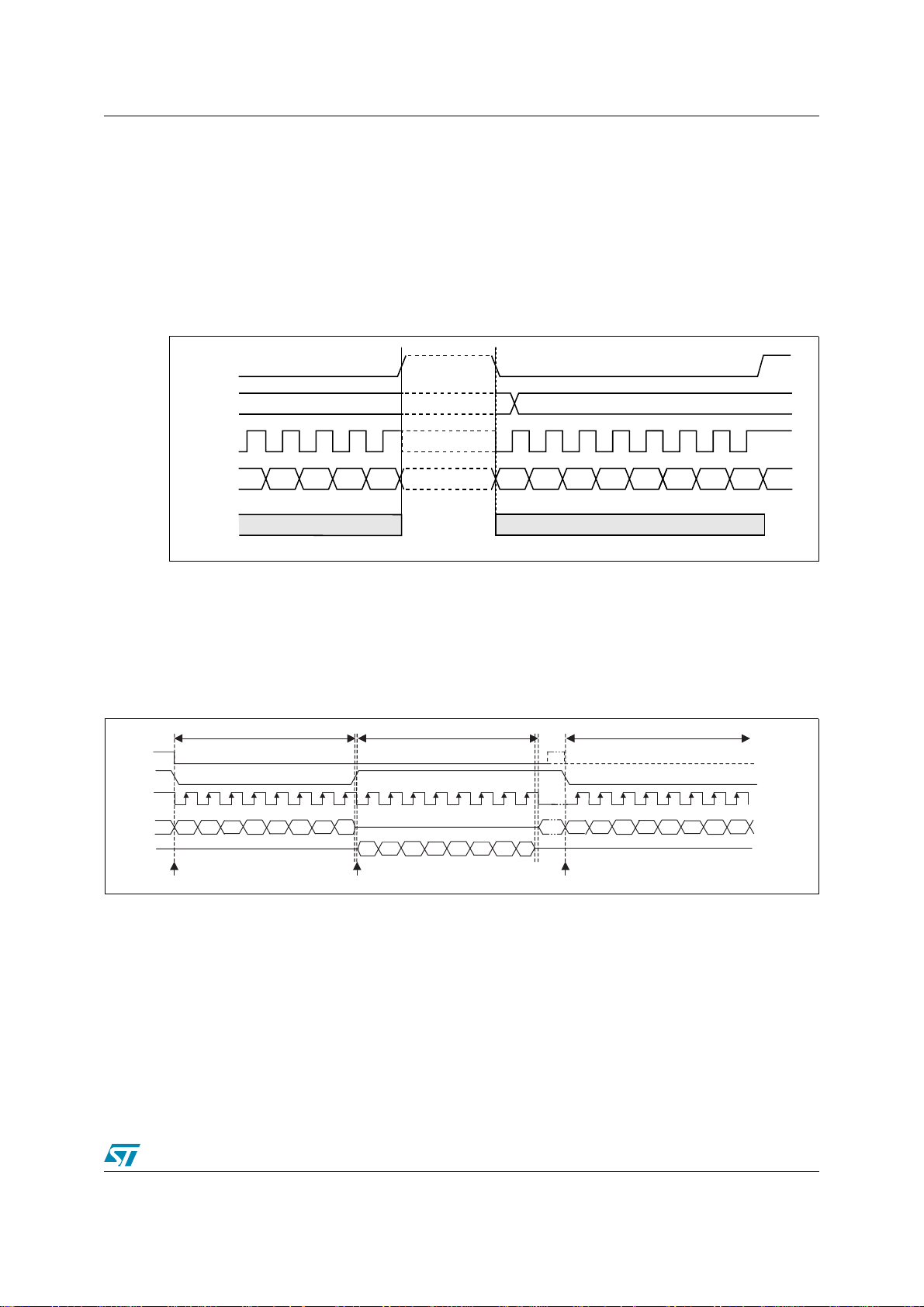
4.4 Reading Mode
STE2007 features a reading Command to transmitt data from the LCD driver to Host
Processor. After the reading command STE2007 transfers 8 bits to the Host controller:
– Identification Byte (Command Code DB
4.4.1 IIdentification byte
Identification byte is an 8 Bit code that identify the module revision Number.
Table 15. ID byte format
Bit nr D7(MSB) D6 D5 D4 D3 D2 D1 D0(LSB)
0 0 I DB PAD I DA PA D 0 0 0 0
Figure 18.
ASIC(MCU)
8 bit register
Power IC
VDD
VDDI
GND
MCU TxData
Driver TxData
VDDCP
VDD
VDDI
VSS
VSSCP
RESET
SDA
XCS
SCLK
test
Auto
return
)
hex
STE2007
Command decoder
Multi
plexer
ID
VLCD
Voltage booster
BaseBand side
Driver side
Figure 19.
Identification Information
Send rading command (DBh)
Read status(ID data)
Send reset command
26/62
LCD Power
Supply circuit
Command:E2H
Page 27
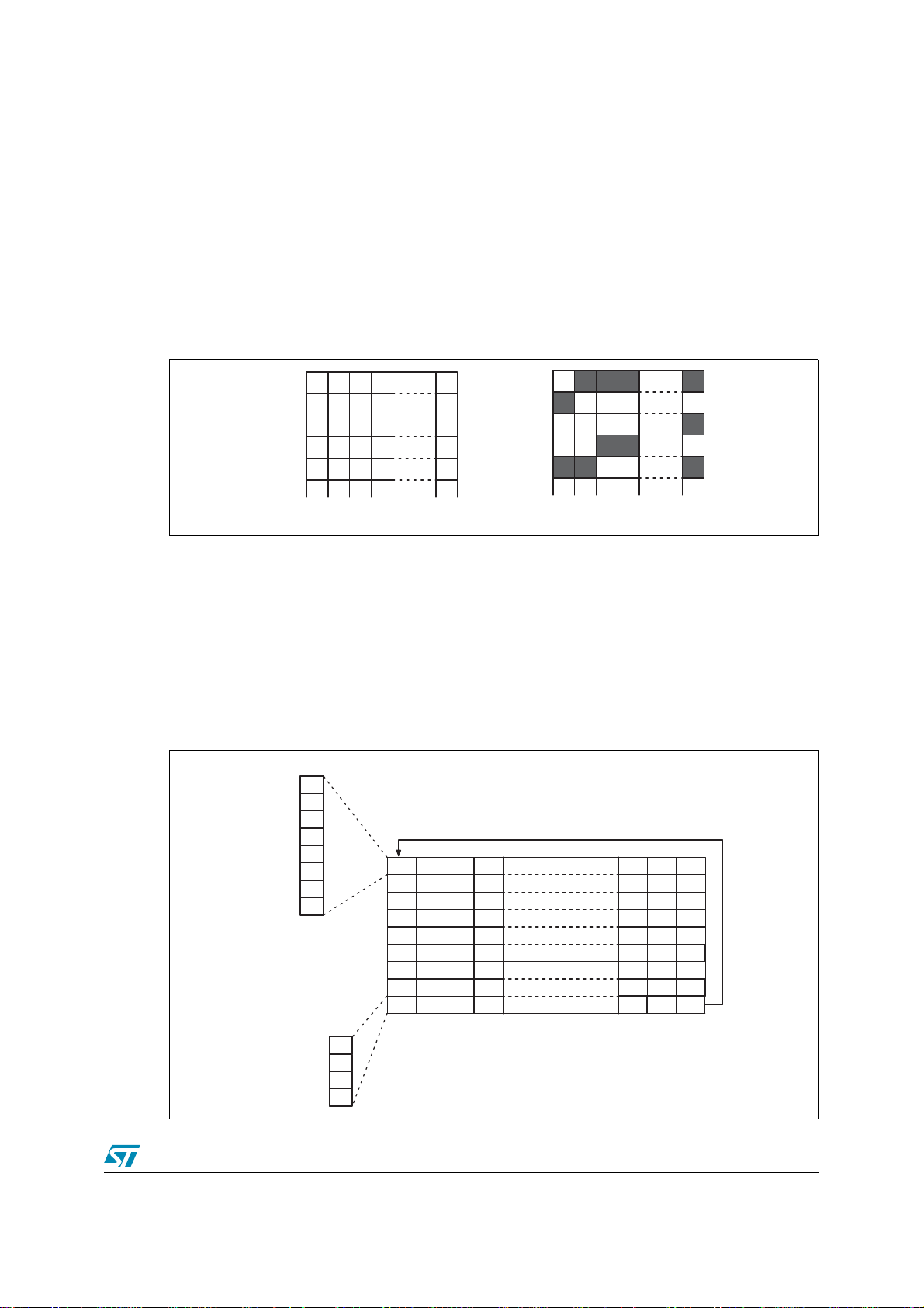
STE2007 5 Display Data RAM (DDRAM)
5 Display Data RAM (DDRAM)
5.1 DDRAM and Page/column address circuit
The DDRAM stores pixel data for LCD. It is a 68–row (8 page by 8 bits +4) by 96–column
addressable array. D7 to D0 display data from MCU corresponds to the LCD common direction.
”0” bit in DDRAM is a OFF–dot on display and ”1” bit in DDRAM is displayed as ON–dot on
display.
Figure 20. DDRAM vs. display on LCD
011 1 1D0
100 0 0D1
000 0 1D2
001 1 0D3
110 0 1D4
±± ±±
DDRAM Display on LCD
COM0
COM1
COM2
COM3
COM4
Each pixel can be selected when page address and column address are specified. The MCU
issues Page address set command to change the page and access to another page. In
DDRAM page address 8 (D3,D2,D1,D0=1,0,0,0) only display data D0,D1,D2 & D3 are valid.
The DDRAM column address is specified by Column address set command.
The specified column address is automatically incremented by +1 when a Display data write
command is entered. After the last column address (5Fh), column address returns to 00h and
page address incremented by +1. After the very last address (column=5Fh, page=8h), both
column address and page address return to 00h (column address=00h, page address=0h).
Figure 21. Column address in normal mode
Data
LSBit
MSBit
Page address
Data for page address 0H to 07H
D0
D1
D2
D3
D4
D5
D6
D7
D0
D1
D2
D3
0 1 2 94 95
0H
96 97 98
1H
192 193 194
2H
3H
288 289 290
4H
384 385 386
5H
480 481 482
576 577 578
6H
672 673 674
7H
768 769 770
8H
00H 01H
Data for page address 8H
02H
Column address
190 191
286 287
382 383
478 479
574 575
670 671
766 767
862 863
5EH 5FH
27/62
Page 28

5 Display Data RAM (DDRAM) STE2007
Figure 22. Column address in reversed mode
Data for page address 0H to 07H
Data
D0
LSBit
D1
D2
D3
95
191
287
383
479
575
671
767
863
5FH
190
286
382
478
574
670
766
862
5EH
94
Column address
02H
0H
96
9798
1H
2H
192193194
3H
288289290
4H
384385386
5H
480481482
576577578
6H
672673674
7H
8H
768769770
00H01H
Data for page address 8H
D4
D5
D6
D7
Page address
D0
D1
D2
D3
MSBit
Data can be written to the DDRAM at the same time as data is being displayed, without causing
the LCD to flicker.
Segment driver direction command can be used to reverse the relationship between the
DDRAM column address and segment output. This function is achieved writing data into
DDRAM in reverse order (from Right to left).
Table 16. Column address direction
Column
address
Normal
Direction
Reverse
Direction
00H 01H 02H 5DH 5EH 5FH 5DH
SEG0 SEG1 SEG2 _ _ _ _ _ _ SEG93 SEG94 SEG95
SEG95 SEG94 SEG93 _ _ _ _ _ _ SEG2 SEG1 SEG0
5.2 Line address circuit
The line address circuit specifies the line address relating to the COM output when the contents
of the DDRAM are displayed. The display start line that is normally the top line of the display,
can be specified by Display start line address set command.
STE2007 features Four different Multiplexing Mode to fine tune the duty ratio on the display
size:
– 68 Lines Display
– 65 Lines Display
– 49 Lines Display
– 33 Lines Display
28/62
Page 29

STE2007 5 Display Data RAM (DDRAM)
Figure 23. 68–line Mode
Page address
D2 D1 D0
D3
0
0
0
0
0
0
1
0
0
1
0
0
0
0
1
0
0
1
1
0
1
1
0
1
0
0
1
Column address
ICONMODE="1"
D
a
t
a
D0
D1
D2
D3
0
D4
D5
D6
D7
D0
D1
D2
D3
1
D4
D5
D6
D7
D0
D1
D2
D3
0
D4
D5
D6
D7
D0
D1
D2
D3
1
D4
D5
D6
D7
D0
D1
D2
D3
0
D4
D5
D6
D7
D0
D1
D2
D3
1
D4
D5
D6
D7
D0
D1
D2
D3
0
D4
D5
D6
D7
D0
D1
D2
D3
1
D4
D5
D6
D7
D0
D1
0
D2
D3
00H
02H 06H03H 04H 05H
01H
Page 0
Page 1
Page 2
Page 3
Page 4
Page 5
Page 6
Page 7
Page 8
59H
5AH
5BH 5FH5CH 5DH 5EH
Line
Address
00H
01H
02H
03H
04H
05H
06H
07H
08H
09H
0AH
0BH
0CH
0DH
0EH
0FH
10H
11H
12H
13H
14H
15H
16H
17H
18H
19H
1AH
1BH
1CH
1DH
1EH
1FH
20H
21H
22H
23H
24H
25H
26H
27H
28H
29H
2AH
2BH
2CH
2DH
2EH
2FH
30H
31H
32H
33H
34H
35H
36H
37H
38H
39H
3AH
3BH
3CH
3DH
3EH
3FH
40H
41H
42H
43H
Start
COM Output
Normal
Reverse
direction
direction
COM66
COM0
COM65
COM1
COM64
COM2
COM3
COM63
COM4
COM62
COM5
COM61
COM6
COM60
COM7
COM59
COM8
COM58
COM9
COM57
COM10
COM56
COM11
COM55
COM12
COM54
COM13
COM53
COM14
COM52
COM15
COM51
COM16
COM50
COM17
COM49
COM18
COM48
COM19
COM47
COM20
COM46
COM21
COM45
COM22
COM44
COM23
COM43
COM24
COM42
COM25
COM41
COM26
COM40
COM27
COM39
COM28
COM38
COM29
COM37
COM30
COM36
COM31
COM35
COM32
COM34
COM33
COM33
COM34
COM32
COM35
COM31
COM36
COM30
COM37
COM29
COM38
COM28
COM39
COM27
COM40
COM26
COM41
COM25
COM42
COM24
COM43
COM23
COM44
COM22
COM45
COM21
COM46
COM20
COM47
COM19
COM48
COM18
COM49
COM17
COM50
COM16
COM51
COM15
COM52
COM14
COM53
COM13
COM54
COM12
COM55
COM1
COM56
COM10
COM57
COM9
COM58
COM8
COM59
COM7
COM60
COM6
COM61
COM5
COM62
COM4
COM63
COM3
COM64
COM2
COM65
COM1
COM66
COM0
COMS COMS
Line
Address
00H
01H
02H
03H
04H
05H
06H
07H
08H
09H
0AH
0BH
0CH
0DH
0EH
0FH
10H
11H
12H
13H
14H
15H
16H
17H
18H
19H
1AH
1BH
1CH
1DH
Start
1EH
1FH
20H
21H
22H
23H
24H
25H
26H
27H
28H
29H
2AH
2BH
2CH
2DH
2EH
2FH
30H
31H
32H
1
33H
34H
35H
36H
37H
38H
39H
3AH
3BH
3CH
3DH
3EH
3FH
40H
41H
42H
43H
ICONMODE="0"
COM Output
Normal
Reverse
direction
direction
COM0
COMS
COM66
COM1
COM65
COM2
COM3
COM64
COM4
COM63
COM5
COM62
COM6
COM61
COM7
COM60
COM8
COM59
COM9
COM58
COM10
COM57
COM11
COM56
COM12
COM55
COM13
COM54
COM14
COM53
COM15
COM52
COM16
COM51
COM17
COM50
COM18
COM49
COM19
COM48
COM20
COM47
COM21
COM46
COM22
COM45
COM23
COM44
COM24
COM43
COM25
COM42
COM26
COM41
COM27
COM40
COM28
COM39
COM29
COM38
COM30
COM37
COM31
COM36
COM32
COM35
COM33
COM34
COM34
COM33
COM35
COM32
COM36
COM31
COM37
COM30
COM38
COM29
COM39
COM28
COM40
COM27
COM41
COM26
COM42
COM25
COM43
COM24
COM44
COM23
COM45
COM22
COM46
COM21
COM47
COM20
COM48
COM19
COM18
COM49
COM50
COM17
COM16
COM51
COM52
COM15
COM53
COM14
COM54
COM13
COM55
COM12
COM56
COM11
COM57
COM10
COM58
COM9
COM59
COM8
COM60
COM7
COM6
COM61
COM5
COM62
COM63
COM4
COM3
COM64
COM2
COM65
COM1
COM66
COM0
COMS
SEG
Output
Normal
Direction
Reverse
Direction
Display start line does not access 65th, 66th, 67th, 68th line
S
S
S
S
S
S
E
E
E
G
G
G
0
1
2
S
S
S
E
E
E
G
G
G
95
94
93
S
E
E
E
E
G
G
G
G
3
4
5
6
S
S
S
S
E
E
E
E
G
G
G
G
92
91
90
89
S
S
S
E
E
E
G
G
G
91
90
89
S
S
S
E
E
E
G
G
G
4
5
6
S
S
S
S
E
E
E
E
G
G
G
G
95
94
93
92
S
S
S
S
E
E
E
E
G
G
G
G
0
1
2
3
Display start line does not access 65th, 66th, 67th, 68th line
29/62
Page 30

5 Display Data RAM (DDRAM) STE2007
Figure 24. 65–line Mode
Page address
D2 D1 D0
D3
0
0
0
0
0
0
1
0
0
1
0
0
0
0
1
0
0
1
1
0
1
1
0
1
0
0
1
Column address
D
a
t
a
D0
D1
D2
D3
0
D4
D5
D6
D7
D0
D1
D2
D3
1
D4
D5
D6
D7
D0
D1
D2
D3
0
D4
D5
D6
D7
D0
D1
D2
D3
1
D4
D5
D6
D7
D0
D1
D2
D3
0
D4
D5
D6
D7
D0
D1
D2
D3
1
D4
D5
D6
D7
D0
D1
D2
D3
0
D4
D5
D6
D7
D0
D1
D2
D3
1
D4
D5
D6
D7
D0
D1
0
D2
D3
00H
02H 06H03H 04H 05H
01H
Page 0
Page 1
Page 2
Page 3
Page 4
Page 5
Page 6
Page 7
Page 8
5AH
59H
5BH 5FH5CH5DH 5EH
Line
Address
00H
01H
02H
03H
04H
05H
06H
07H
08H
09H
0AH
0BH
0CH
0DH
0EH
0FH
10H
11H
12H
13H
14H
15H
16H
17H
18H
19H
1AH
1BH
1CH
1DH
Start
1EH
1FH
20H
21H
22H
23H
24H
25H
26H
27H
28H
29H
2AH
2BH
2CH
2DH
2EH
2FH
30H
31H
32H
33H
34H
35H
36H
37H
38H
39H
3AH
3BH
3CH
3DH
3EH
3FH
40H
41H
42H
43H
Display start line does not access 65th, 66th, 67th, 68th line
COM Output
Normal
Reverse
direction
direction
COM0
COM63
COM1
COM62
COM2
COM61
COM3
COM60
COM4
COM59
COM5
COM58
COM6
COM57
COM7
COM56
COM8
COM55
COM9
COM54
COM10
COM53
COM11
COM52
COM12
COM51
COM13
COM50
COM14
COM49
COM15
COM48
COM16
COM47
COM17
COM46
COM18
COM45
COM19
COM44
COM20
COM43
COM21
COM42
COM22
COM41
COM23
COM40
COM24
COM39
COM25
COM38
COM26
COM37
COM27
COM36
COM28
COM35
COM29
COM34
COM30
COM33
COM31
COM32
COM32
COM31
COM33
COM30
COM34
COM29
COM35
COM28
COM36
COM27
COM37
COM26
COM38
COM25
COM39
COM24
COM40
COM23
COM41
COM22
COM42
COM21
COM43
COM20
COM44
COM19
COM45
COM18
COM46
COM17
COM47
COM16
COM48
COM15
COM49
COM14
COM50
COM13
COM51
COM12
COM52
COM11
COM53
COM10
COM54
COM9
COM55
COM8
COM56
COM7
COM57
COM6
COM58
COM5
COM59
COM4
COM60
COM3
COM61
COM2
COM1
COM62
COM63
COM0
COM64 COM64
Line
Address
00H
01H
02H
03H
04H
05H
06H
07H
08H
09H
0AH
0BH
0CH
0DH
0EH
0FH
10H
11H
12H
13H
14H
15H
16H
17H
18H
19H
1AH
1BH
1CH
1DH
1EH
1FH
20H
21H
22H
23H
24H
25H
26H
27H
28H
29H
2AH
2BH
2CH
2DH
2EH
2FH
30H
31H
32H
33H
34H
35H
36H
37H
38H
39H
3AH
3BH
3CH
3DH
3EH
3FH
40H
41H
42H
43H
Start
ICONMODE="1"
ICONMODE="0"
COM Output
Normal
Reverse
direction
direction
COM64
COM0
COM1
COM63
COM2
COM62
COM3
COM61
COM4
COM60
COM5
COM59
COM6
COM58
COM7
COM57
COM8
COM56
COM9
COM55
COM10
COM54
COM11
COM53
COM12
COM52
COM13
COM51
COM14
COM50
COM15
COM49
COM16
COM48
COM17
COM47
COM18
COM46
COM19
COM45
COM20
COM44
COM21
COM43
COM22
COM42
COM23
COM41
COM24
COM40
COM25
COM39
COM26
COM38
COM27
COM37
COM28
COM36
COM29
COM35
COM30
COM34
COM31
COM33
COM32
COM32
COM33
COM31
COM34
COM30
COM35
COM29
COM36
COM28
COM37
COM27
COM38
COM26
COM39
COM25
COM40
COM24
COM41
COM23
COM42
COM22
COM43
COM21
COM44
COM20
COM45
COM19
COM46
COM18
COM47
COM17
COM48
COM16
COM49
COM15
COM50
COM14
COM51
COM13
COM52
COM12
COM53
COM11
COM54
COM10
COM55
COM9
COM56
COM8
COM57
COM7
COM58
COM6
COM59
COM5
COM60
COM4
COM61
COM3
COM62
COM2
COM63
COM1
COM64
COM0
SEG
Output
Normal
Direction
Reverse
Direction
S
S
S
S
S
S
E
E
E
G
G
G
0
1
2
S
S
S
E
E
E
G
G
G
95
94
93
S
E
E
E
E
G
G
G
G
3
4
5
6
S
S
S
S
E
E
E
E
G
G
G
G
92
91
90
89
S
S
S
E
E
E
G
G
G
91
90
89
S
S
S
E
E
E
G
G
G
4
5
6
S
S
S
S
E
E
E
E
G
G
G
G
95
94
93
92
S
S
S
S
E
E
E
E
G
G
G
G
0
1
2
3
30/62
Page 31

STE2007 5 Display Data RAM (DDRAM)
Figure 25. 49–line Mode
Page address
D2 D1 D0
D3
0
0
0
0
0
0
1
0
0
1
0
0
0
0
1
0
0
1
1
0
1
1
0
1
0
0
1
Column address
D
a
t
a
D0
D1
D2
D3
0
D4
D5
D6
D7
D0
D1
D2
D3
1
D4
D5
D6
D7
D0
D1
D2
D3
0
D4
D5
D6
D7
D0
D1
D2
D3
1
D4
D5
D6
D7
D0
D1
D2
D3
0
D4
D5
D6
D7
D0
D1
D2
D3
1
D4
D5
D6
D7
D0
D1
D2
D3
0
D4
D5
D6
D7
D0
D1
D2
D3
1
D4
D5
D6
D7
D0
D1
0
D2
D3
00H
02H 06H03H 04H 05H
01H
Page 0
Page 1
Page 2
Page 3
Page 4
Page 5
Page 6
Page 7
Page 8
59H
5AH
5BH 5FH5CH5DH 5EH
Line
Address
00H
01H
02H
03H
04H
05H
06H
07H
08H
09H
0AH
0BH
0CH
0DH
0EH
0FH
10H
11H
12H
13H
14H
15H
16H
17H
18H
19H
1AH
1BH
1CH
1DH
Start
1EH
1FH
20H
21H
22H
23H
24H
25H
26H
27H
28H
29H
2AH
2BH
2CH
2DH
2EH
2FH
30H
31H
32H
33H
34H
35H
36H
37H
38H
39H
3AH
3BH
3CH
3DH
3EH
3FH
40H
41H
42H
43H
Display start line does not access 65th, 66th, 67th, 68th line
COM Output
Normal
Reverse
direction
direction
COM0
COM47
COM1
COM46
COM2
COM45
COM3
COM44
COM4
COM43
COM5
COM42
COM6
COM41
COM7
COM40
COM8
COM39
COM9
COM38
COM10
COM37
COM11
COM36
COM12
COM35
COM13
COM34
COM14
COM33
COM15
COM32
COM16
COM31
COM17
COM30
COM18
COM29
COM19
COM28
COM20
COM27
COM21
COM26
COM22
COM25
COM23
COM24
COM24
COM23
COM25
COM22
COM26
COM21
COM27
COM20
COM28
COM19
COM29
COM18
COM30
COM17
COM31
COM16
COM32
COM15
COM33
COM14
COM34
COM13
COM35
COM12
COM36
COM11
COM37
COM10
COM38
COM9
COM39
COM8
COM40
COM7
COM41
COM6
COM42
COM5
COM43
COM4
COM44
COM3
COM45
COM2
COM46
COM1
COM47
COM0
COM64 COM64
Line
Address
00H
01H
02H
03H
04H
05H
06H
07H
08H
09H
0AH
0BH
0CH
0DH
0EH
0FH
10H
11H
12H
13H
14H
15H
16H
17H
18H
19H
1AH
1BH
1CH
1DH
1EH
1FH
20H
21H
22H
23H
24H
25H
26H
27H
28H
29H
2AH
2BH
2CH
2DH
2EH
2FH
30H
31H
32H
33H
34H
35H
36H
37H
38H
39H
3AH
3BH
3CH
3DH
3EH
3FH
40H
41H
42H
43H
Start
ICONMODE="1"
ICONMODE="0"
COM Output
Normal
Reverse
direction
direction
COM0
COM48
COM47
COM1
COM46
COM2
COM45
COM3
COM44
COM4
COM43
COM5
COM42
COM6
COM41
COM7
COM40
COM8
COM39
COM9
COM38
COM10
COM37
COM11
COM36
COM12
COM35
COM13
COM34
COM14
COM33
COM15
COM32
COM16
COM31
COM17
COM30
COM18
COM29
COM19
COM28
COM20
COM27
COM21
COM26
COM22
COM25
COM23
COM24
COM24
COM23
COM25
COM22
COM26
COM21
COM27
COM20
COM28
COM19
COM29
COM18
COM30
COM17
COM31
COM16
COM32
COM15
COM33
COM14
COM34
COM13
COM35
COM12
COM36
COM11
COM37
COM10
COM38
COM9
COM39
COM8
COM40
COM7
COM41
COM6
COM42
COM5
COM43
COM4
COM44
COM3
COM45
COM2
COM46
COM1
COM47
COM0
COM48
SEG
Output
Normal
Direction
Reverse
Direction
S
S
S
S
S
S
E
E
E
G
G
G
0
1
2
S
S
S
E
E
E
G
G
G
95
94
93
S
E
E
E
E
G
G
G
G
3
4
5
6
S
S
S
S
E
E
E
E
G
G
G
G
92
91
90
89
S
S
S
E
E
E
G
G
G
91
90
89
S
S
S
E
E
E
G
G
G
4
5
6
S
S
S
S
E
E
E
E
G
G
G
G
95
94
93
92
S
S
S
S
E
E
E
E
G
G
G
G
0
1
2
3
31/62
Page 32

5 Display Data RAM (DDRAM) STE2007
Figure 26. 33–line Mode
Page address
D2 D1 D0
D3
0
0
0
0
0
0
1
0
0
1
0
0
0
0
1
0
0
1
1
0
1
1
0
1
0
0
1
Column address
D
a
t
a
D0
D1
D2
D3
0
D4
D5
D6
D7
D0
D1
D2
D3
1
D4
D5
D6
D7
D0
D1
D2
D3
0
D4
D5
D6
D7
D0
D1
D2
1
D3
D4
D5
D6
D7
D0
D1
D2
D3
0
D4
D5
D6
D7
D0
D1
D2
D3
1
D4
D5
D6
D7
D0
D1
D2
D3
0
D4
D5
D6
D7
D0
D1
D2
D3
D4
1
D5
D6
D7
D0
D1
0
D2
D3
00H
02H 06H03H 04H 05H
01H
Page 0
Page 1
Page 2
Page 3
Page 4
Page 5
Page 6
Page 7
Page 8
59H
5AH
5BH 5FH5CH5DH 5EH
Line
Address
00H
01H
02H
03H
04H
05H
06H
07H
08H
09H
0AH
0BH
0CH
0DH
0EH
0FH
10H
11H
12H
13H
14H
15H
16H
17H
18H
19H
1AH
1BH
1CH
1DH
Start
1EH
1FH
20H
21H
22H
23H
24H
25H
26H
27H
28H
29H
2AH
2BH
2CH
2DH
2EH
2FH
30H
31H
32H
33H
34H
35H
36H
37H
38H
39H
3AH
3BH
3CH
3DH
3EH
3FH
40H
41H
42H
43H
Display start line does not access 65th, 66th, 67th, 68th line
COM Output
Normal
Reverse
direction
direction
COM0
COM31
COM1
COM30
COM2
COM29
COM3
COM28
COM4
COM27
COM5
COM26
COM6
COM25
COM7
COM24
COM8
COM23
COM9
COM22
COM10
COM21
COM11
COM20
COM12
COM19
COM13
COM18
COM14
COM17
COM15
COM16
COM16
COM15
COM17
COM14
COM18
COM13
COM19
COM12
COM20
COM11
COM21
COM10
COM22
COM9
COM23
COM8
COM24
COM7
COM25
COM6
COM26
COM5
COM27
COM4
COM28
COM3
COM29
COM2
COM30
COM1
COM31
COM0
COM64 COM64
Line
Address
00H
01H
02H
03H
04H
05H
06H
07H
08H
09H
0AH
0BH
0CH
0DH
0EH
0FH
10H
11H
12H
13H
14H
15H
16H
17H
18H
19H
1AH
1BH
1CH
1DH
1EH
1FH
20H
21H
22H
23H
24H
25H
26H
27H
28H
29H
2AH
2BH
2CH
2DH
2EH
2FH
30H
31H
32H
33H
34H
35H
36H
37H
38H
39H
3AH
3BH
3CH
3DH
3EH
3FH
40H
41H
42H
43H
Start
ICONMODE="1"
ICONMODE="0"
COM Output
Normal
Reverse
direction
direction
COM32
COM0
COM31
COM1
COM30
COM2
COM29
COM3
COM28
COM4
COM27
COM5
COM26
COM6
COM25
COM7
COM24
COM8
COM23
COM9
COM22
COM10
COM21
COM11
COM20
COM12
COM19
COM13
COM18
COM14
COM17
COM15
COM16
COM16
COM17
COM15
COM18
COM14
COM19
COM13
COM20
COM12
COM21
COM11
COM22
COM10
COM23
COM9
COM24
COM8
COM25
COM7
COM26
COM6
COM27
COM5
COM28
COM4
COM29
COM3
COM30
COM2
COM31
COM1
COM0
COM32
SEG
Output
Normal
Direction
Reverse
Direction
S
S
S
S
S
S
E
E
E
G
G
G
0
1
2
S
S
S
E
E
E
G
G
G
95
94
93
S
E
E
E
E
G
G
G
G
3
4
5
6
S
S
S
S
E
E
E
E
G
G
G
G
92
91
90
89
S
S
S
E
E
E
G
G
G
91
90
89
S
S
S
E
E
E
G
G
G
4
5
6
S
S
S
S
E
E
E
E
G
G
G
G
95
94
93
92
S
S
S
S
E
E
E
E
G
G
G
G
0
1
2
3
5.3 Partial Display
STE2007 feature four configuration for Partial Display function:
– 33 Line Partial Display
– 25 Line Partial display
– 16 Line Partial Display
– 9 Line Partial Display
Partial display Area location on the screen is defined by Image Location Parameter.
Image Location + Partial display area > Multiplexing rate.
32/62
Page 33

STE2007 5 Display Data RAM (DDRAM)
Figure 27.
Display
Image Location + Partial display area width <= Multiplexing rate Image Location + Partial display area width > Multiplexing rate
When Partial Display Mode is enabled the user has to Update the Operative Voltage, Bias Ratio
and Charge Pump Setting to match the new working conditions.
5.3.1 33 Line Partial Display Mode
Partial Display Area is composed of 33 Lines. Memory vs. Row Drivers Mapping is defined
according to the following parameters:
– Multiplexing Value
– IL[2:0]
Figure 28. Example: Partial Display 33 lines & MUX65
D
Page address
D2 D1 D0
D3
0
0
0
0
0
0
1
0
0
1
0
0
0
0
1
0
0
1
1
0
1
1
0
1
0
0
1
Column address
a
t
a
D0
D1
D2
D3
0
D4
D5
D6
D7
D0
D1
D2
D3
1
D4
D5
D6
D7
D0
D1
D2
D3
0
D4
D5
D6
D7
D0
D1
D2
D3
1
D4
D5
D6
D7
D0
D1
D2
D3
0
D4
D5
D6
D7
D0
D1
D2
D3
1
D4
D5
D6
D7
D0
D1
D2
D3
0
D4
D5
D6
D7
D0
D1
D2
D3
1
D4
D5
D6
D7
D0
D1
0
D2
D3
00H
02H 06H03H 04H 05H
01H
Page 0
Page 1
Page 2
Page 3
Page 4
Page 5
Page 6
Page 7
Page 8
59H
5AH
5BH 5FH5CH 5DH 5EH
Line
Address
00H
01H
02H
03H
04H
05H
06H
07H
IL[2:0]
08H
09H
0AH
0BH
0CH
0DH
0EH
0FH
10H
11H
12H
13H
14H
15H
16H
17H
18H
19H
1AH
1BH
1CH
1DH
Start
1EH
1FH
20H
21H
22H
23H
24H
25H
26H
27H
28H
29H
2AH
2BH
2CH
2DH
2EH
2FH
30H
31H
32H
33H
34H
35H
36H
37H
38H
39H
3AH
3BH
3CH
3DH
3EH
3FH
40H
41H
42H
43H
Display start line does not access 65th, 66th, 67th, 68th line
ICONMODE="1"
COM Output
Normal
Reverse
direction
direction
COM0
COM63
COM1
COM62
COM2
COM61
COM3
COM60
COM4
COM59
COM5
COM58
COM6
COM57
COM7
COM56
COM8
COM55
COM9
COM54
COM10
COM53
COM11
COM52
COM12
COM51
COM13
COM50
COM14
COM49
COM15
COM48
COM16
COM47
COM17
COM46
COM18
COM45
COM19
COM44
COM20
COM43
COM21
COM42
COM22
COM41
COM23
COM40
COM24
COM39
COM25
COM38
COM26
COM37
COM27
COM36
COM28
COM35
COM29
COM34
COM30
COM33
COM31
COM32
COM32
COM31
COM33
COM30
COM34
COM29
COM35
COM28
COM36
COM27
COM37
COM26
COM38
COM25
COM39
COM24
COM40
COM23
COM41
COM22
COM42
COM21
COM43
COM20
COM44
COM19
COM45
COM18
COM46
COM17
COM47
COM16
COM48
COM15
COM49
COM14
COM50
COM13
COM51
COM12
COM52
COM11
COM53
COM10
COM54
COM9
COM55
COM8
COM56
Partial Display Area (32 +1)
COM7
COM57
COM6
COM58
COM5
COM59
COM4
COM60
COM3
COM61
COM2
COM1
COM62
COM63
COM0
COMS0 COMS0
Line
Address
00H
01H
02H
03H
04H
05H
06H
07H
08H
09H
0AH
0BH
0CH
0DH
0EH
0FH
10H
11H
12H
13H
14H
15H
16H
17H
18H
19H
1AH
1BH
1CH
1DH
1EH
1FH
20H
21H
22H
23H
24H
25H
26H
27H
28H
29H
2AH
2BH
2CH
2DH
2EH
2FH
30H
31H
32H
33H
34H
35H
36H
37H
38H
39H
3AH
3BH
3CH
3DH
3EH
3FH
40H
41H
42H
43H
IL[2:0]
Start
Display
ICONMODE="0"
Normal
direction
Partial Display Area (33)
COM Output
COM0
COM1
COM2
COM3
COM4
COM5
COM6
COM7
COM8
COM9
COM10
COM11
COM12
COM13
COM14
COM15
COM16
COM17
COM18
COM19
COM20
COM21
COM22
COM23
COM24
COM25
COM26
COM27
COM28
COM29
COM30
COM31
COM32
COM33
COM34
COM35
COM36
COM37
COM38
COM39
COM40
COM41
COM42
COM43
COM44
COM45
COM46
COM47
COM48
COM49
COM50
COM51
COM52
COM53
COM54
COM55
COM56
COM57
COM58
COM59
COM60
COM61
COM62
COM63
COMS0
Reverse
direction
COMS0
COM63
COM62
COM61
COM60
COM59
COM58
COM57
COM56
COM55
COM54
COM53
COM52
COM51
COM50
COM49
COM48
COM47
COM46
COM45
COM44
COM43
COM42
COM41
COM40
COM39
COM38
COM37
COM36
COM35
COM34
COM33
COM32
COM31
COM30
COM29
COM28
COM27
COM26
COM25
COM24
COM23
COM22
COM21
COM20
COM19
COM18
COM17
COM16
COM15
COM14
COM13
COM12
COM11
COM10
COM9
COM8
COM7
COM6
COM5
COM4
COM3
COM2
COM1
COM0
SEG
Output
Normal
Direction
Reverse
Direction
S
S
S
S
S
S
E
E
G
G
0
1
S
S
E
E
G
G
95
94
S
E
E
E
E
E
G
G
G
G
G
2
3
4
5
6
S
S
S
S
S
E
E
E
E
E
G
G
G
G
G
93
92
91
90
89
S
S
E
E
G
G
90
89
S
S
E
E
G
G
5
6
S
S
S
S
S
E
E
E
E
E
G
G
G
G
G
95
94
93
92
91
S
S
S
S
S
E
E
E
E
E
G
G
G
G
G
0
1
2
3
4
33/62
Page 34
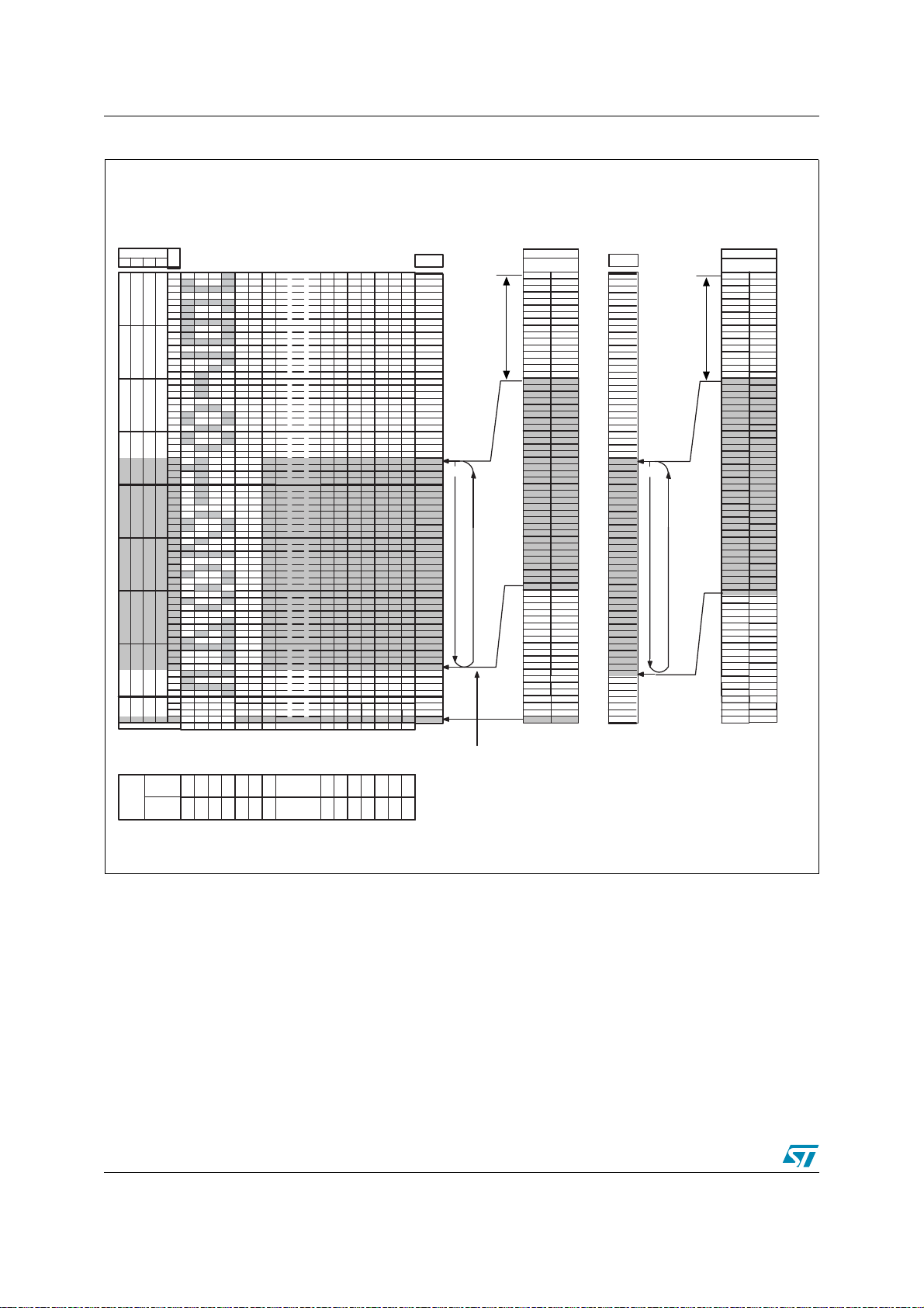
5 Display Data RAM (DDRAM) STE2007
Figure 29. Example: Partial Display 33 lines & MUX68
Page address
D2 D1 D0
D3
0
0
0
0
0
0
1
0
0
1
0
0
0
0
1
0
0
1
1
0
1
1
0
1
0
0
1
Column address
Normal
Direction
SEG
Output
Reverse
Direction
ICONMODE="1"
D
a
t
a
D0
D1
D2
D3
0
D4
D5
D6
D7
D0
D1
D2
D3
1
D4
D5
D6
D7
D0
D1
D2
D3
0
D4
D5
D6
D7
D0
D1
D2
D3
1
D4
D5
D6
D7
D0
D1
D2
D3
0
D4
D5
D6
D7
D0
D1
D2
D3
1
D4
D5
D6
D7
D0
D1
D2
D3
0
D4
D5
D6
D7
D0
D1
D2
D3
1
D4
D5
D6
D7
D0
D1
0
D2
D3
00H
02H 06H03H 04H 05H
01H
S
S
S
S
E
G
0
S
E
G
95
S
E
E
E
E
G
G
G
G
1
2
3
4
S
S
S
S
E
E
E
E
G
G
G
G
94
93
92
91
Page 0
Page 1
Page 2
Page 3
Page 4
Page 5
Page 6
Page 7
Page 8
5AH
59H
5BH 5FH5CH5DH 5EH
S
S
E
E
G
G
5
6
S
S
E
E
G
G
90
89
S
S
S
S
E
E
E
E
G
G
G
G
92
91
90
89
S
S
S
S
E
E
E
E
G
G
G
G
3
4
5
6
Line
Address
00H
01H
02H
03H
04H
05H
06H
07H
IL[2:0]
08H
09H
0AH
0BH
0CH
0DH
0EH
0FH
10H
11H
12H
13H
14H
15H
16H
17H
18H
19H
1AH
1BH
1CH
1DH
Start
1EH
1FH
20H
21H
22H
23H
24H
25H
26H
27H
28H
29H
2AH
2BH
2CH
2DH
2EH
2FH
30H
31H
32H
33H
34H
35H
36H
37H
38H
39H
3AH
3BH
3CH
3DH
3EH
3FH
40H
41H
42H
43H
Display start line does not access 65th, 66th, 67th, 68th line
S
S
S
E
E
E
G
G
G
95
94
93
S
S
S
E
E
E
G
G
G
0
1
2
COM Output
Normal
Reverse
direction
direction
COM66
COM0
COM65
COM1
COM64
COM2
COM3
COM63
COM4
COM62
COM5
COM61
COM6
COM60
COM7
COM59
COM8
COM58
COM9
COM57
COM10
COM56
COM11
COM55
COM12
COM54
COM13
COM53
COM14
COM52
COM15
COM51
COM16
COM50
COM17
COM49
COM18
COM48
COM19
COM47
COM20
COM46
COM21
COM45
COM22
COM44
COM23
COM43
COM24
COM42
COM25
COM41
COM26
COM40
COM27
COM39
COM28
COM38
COM29
COM37
COM30
COM36
COM31
COM35
COM32
COM34
COM33
COM33
COM34
COM32
COM35
COM31
COM36
COM30
COM37
COM29
COM38
COM28
COM39
COM27
COM40
COM26
COM41
COM25
COM42
COM24
COM43
COM23
COM44
COM22
COM45
COM21
COM46
COM20
COM47
COM19
COM48
COM18
COM49
COM17
COM50
COM16
COM51
COM15
COM52
1
COM14
COM53
COM13
COM54
COM12
COM55
COM1
COM56
Partial Display Area (32 +1)
COM10
COM57
COM9
COM58
COM8
COM59
COM7
COM60
COM6
COM61
COM5
COM62
COM4
COM63
COM3
COM64
COM2
COM65
COM1
COM66
COM0
COMS COMS
Line
Address
00H
01H
02H
03H
04H
05H
06H
07H
08H
09H
0AH
0BH
0CH
0DH
0EH
0FH
10H
11H
12H
13H
14H
15H
16H
17H
18H
19H
1AH
1BH
1CH
1DH
1EH
1FH
20H
21H
22H
23H
24H
25H
26H
27H
28H
29H
2AH
2BH
2CH
2DH
2EH
2FH
30H
31H
32H
33H
34H
35H
36H
37H
38H
39H
3AH
3BH
3CH
3DH
3EH
3FH
40H
41H
42H
43H
IL[2:0]
Start
ICONMODE="0"
COM Output
Normal
direction
COM0
COM1
COM2
COM3
COM4
COM5
COM6
COM7
COM8
COM9
COM10
COM11
COM12
COM13
COM14
COM15
COM16
COM17
COM18
COM19
COM20
COM21
COM22
COM23
COM24
COM25
COM26
COM27
COM28
COM29
COM30
COM31
COM32
COM33
COM34
COM35
COM36
COM37
COM38
COM39
COM40
COM41
COM42
COM43
COM44
COM45
COM46
COM47
COM48
COM49
COM50
COM51
COM52
COM53
Partial Display Area (33)
COM54
COM55
COM56
COM57
COM58
COM59
COM60
COM61
COM62
COM63
COM64
COM65
COM66
COMS
Reverse
direction
COMS
COM66
COM65
COM64
COM63
COM62
COM61
COM60
COM59
COM58
COM57
COM56
COM55
COM54
COM53
COM52
COM51
COM50
COM49
COM48
COM47
COM46
COM45
COM44
COM43
COM42
COM41
COM40
COM39
COM38
COM37
COM36
COM35
COM34
COM33
COM32
COM31
COM30
COM29
COM28
COM27
COM26
COM25
COM24
COM23
COM22
COM21
COM20
COM19
COM18
COM17
COM16
COM15
COM14
COM13
COM12
COM11
COM10
COM9
COM8
COM7
COM6
COM5
COM4
COM3
COM2
COM1
COM0
34/62
Page 35

STE2007 5 Display Data RAM (DDRAM)
5.3.2 25 Line Partial Display Mode
Partial Display Area is composed of 25 Lines. Memory vs. Row Drivers Mapping is defined
according to the following parameters:
– Multiplexing Value
– IL[2:0]
Figure 30. Example: Partial Display 25 lines & MUX65
Page address
D2 D1 D0
D3
0
0
0
0
0
0
1
0
0
1
0
0
0
0
1
0
0
1
1
0
1
1
0
1
0
0
1
Column address
ICONMODE="1"
D
a
t
a
D0
D1
D2
D3
0
D4
D5
D6
D7
D0
D1
D2
D3
1
D4
D5
D6
D7
D0
D1
D2
D3
0
D4
D5
D6
D7
D0
D1
D2
D3
1
D4
D5
D6
D7
D0
D1
D2
D3
0
D4
D5
D6
D7
D0
D1
D2
D3
1
D4
D5
D6
D7
D0
D1
D2
D3
0
D4
D5
D6
D7
D0
D1
D2
D3
1
D4
D5
D6
D7
D0
D1
0
D2
D3
00H
02H 06H03H 04H 05H
01H
Page 0
Page 1
Page 2
Page 3
Page 4
Page 5
Page 6
Page 7
Page 8
5AH
59H
5BH 5FH5CH 5DH 5EH
Line
Address
00H
01H
02H
03H
04H
05H
06H
07H
IL[2:0]
08H
09H
0AH
0BH
0CH
0DH
0EH
0FH
10H
11H
12H
13H
14H
15H
16H
17H
18H
19H
1AH
1BH
1CH
1DH
Start
1EH
1FH
20H
21H
22H
23H
24H
25H
26H
27H
28H
29H
2AH
2BH
2CH
2DH
2EH
2FH
30H
31H
32H
33H
34H
35H
36H
37H
38H
39H
3AH
3BH
3CH
3DH
3EH
3FH
40H
41H
42H
43H
Display start line does not access 65th, 66th, 67th, 68th line
(24 +1)
Partial Display Area
COM Output
Normal
Reverse
direction
direction
COM0
COM63
COM1
COM62
COM2
COM61
COM3
COM60
COM4
COM59
COM5
COM58
COM6
COM57
COM7
COM56
COM8
COM55
COM9
COM54
COM10
COM53
COM11
COM52
COM12
COM51
COM13
COM50
COM14
COM49
COM15
COM48
COM16
COM47
COM17
COM46
COM18
COM45
COM19
COM44
COM20
COM43
COM21
COM42
COM22
COM41
COM23
COM40
COM24
COM39
COM25
COM38
COM26
COM37
COM27
COM36
COM28
COM35
COM29
COM34
COM30
COM33
COM31
COM32
COM32
COM31
COM33
COM30
COM34
COM29
COM35
COM28
COM36
COM27
COM37
COM26
COM38
COM25
COM39
COM24
COM40
COM23
COM41
COM22
COM42
COM21
COM43
COM20
COM44
COM19
COM45
COM18
COM46
COM17
COM47
COM16
COM48
COM15
COM49
COM14
COM50
COM13
COM51
COM12
COM52
COM11
COM53
COM10
COM54
COM9
COM55
COM8
COM56
COM7
COM57
COM6
COM58
COM5
COM59
COM4
COM60
COM3
COM61
COM2
COM1
COM62
COM63
COM0
COM64 COM64
Line
Address
00H
01H
02H
03H
04H
05H
06H
07H
08H
09H
0AH
0BH
0CH
0DH
0EH
0FH
10H
11H
12H
13H
14H
15H
16H
17H
18H
19H
1AH
1BH
1CH
1DH
1EH
1FH
20H
21H
22H
23H
24H
25H
26H
27H
28H
29H
2AH
2BH
2CH
2DH
2EH
2FH
30H
31H
32H
33H
34H
35H
36H
37H
38H
39H
3AH
3BH
3CH
3DH
3EH
3FH
40H
41H
42H
43H
IL[2:0]
Start
ICONMODE="0"
COM Output
Normal
direction
COM0
COM1
COM2
COM3
COM4
COM5
COM6
COM7
COM8
COM9
COM10
COM11
COM12
COM13
COM14
COM15
COM16
COM17
COM18
COM19
COM20
COM21
COM22
COM23
COM24
COM25
COM26
COM27
COM28
COM29
COM30
COM31
COM32
COM33
(25)
COM34
COM35
COM36
COM37
COM38
COM39
COM40
COM41
COM42
COM43
COM44
COM45
COM46
COM47
COM48
COM49
Partial Display Area
COM50
COM51
COM52
COM53
COM54
COM55
COM56
COM57
COM58
COM59
COM60
COM61
COM62
COM63
COM64
Reverse
direction
COM64
COM63
COM62
COM61
COM60
COM59
COM58
COM57
COM56
COM55
COM54
COM53
COM52
COM51
COM50
COM49
COM48
COM47
COM46
COM45
COM44
COM43
COM42
COM41
COM40
COM39
COM38
COM37
COM36
COM35
COM34
COM33
COM32
COM31
COM30
COM29
COM28
COM27
COM26
COM25
COM24
COM23
COM22
COM21
COM20
COM19
COM18
COM17
COM16
COM15
COM14
COM13
COM12
COM11
COM10
COM9
COM8
COM7
COM6
COM5
COM4
COM3
COM2
COM1
COM0
IMAGE lOCATION (IL[2:0]) + Partial display Area Width (19
S
S
S
S
S
S
SEG
Output
Normal
Direction
Reverse
Direction
E
E
E
G
G
G
0
1
2
S
S
S
E
E
E
G
G
G
95
94
93
S
E
E
E
E
G
G
G
G
3
4
5
6
S
S
S
S
E
E
E
E
G
G
G
G
92
91
90
89
S
S
S
S
E
E
E
E
G
G
G
G
92
91
90
89
S
S
S
S
E
E
E
E
G
G
G
G
3
4
5
6
) <= Multiplexing Rate (40
hex
S
S
S
E
E
E
G
G
G
95
94
93
S
S
S
E
E
E
G
G
G
0
1
2
35/62
hex
)
Page 36

5 Display Data RAM (DDRAM) STE2007
5.3.3 17 Line Partial Display Mode
Partial Display Area is composed of 17 Lines. Memory vs. Row Drivers Mapping is defined
according to the following parameters:
– Multiplexing Value
– IL[2:0]
Figure 31. Partial Display 17 Lines
Page address
D2 D1 D0
D3
0
0
0
0
0
0
1
0
0
1
0
0
0
0
1
0
0
1
1
0
1
1
0
1
0
0
1
Column address
ICONMODE="1"
D
a
t
a
D0
D1
D2
D3
0
D4
D5
D6
D7
D0
D1
D2
D3
1
D4
D5
D6
D7
D0
D1
D2
D3
0
D4
D5
D6
D7
D0
D1
D2
D3
1
D4
D5
D6
D7
D0
D1
D2
D3
0
D4
D5
D6
D7
D0
D1
D2
D3
1
D4
D5
D6
D7
D0
D1
D2
D3
0
D4
D5
D6
D7
D0
D1
D2
D3
1
D4
D5
D6
D7
D0
D1
0
D2
D3
00H
02H 06H03H 04H 05H
01H
Page 0
Page 1
Page 2
Page 3
Page 4
Page 5
Page 6
Page 7
Page 8
5AH
59H
5BH 5FH5CH 5DH 5EH
Line
Address
00H
01H
02H
03H
04H
05H
06H
07H
IL[2:0]
08H
09H
0AH
0BH
0CH
0DH
0EH
0FH
10H
11H
12H
13H
14H
15H
16H
17H
18H
19H
1AH
1BH
1CH
1DH
Start
1EH
1FH
20H
21H
22H
23H
24H
25H
26H
27H
28H
29H
2AH
2BH
2CH
2DH
2EH
2FH
30H
31H
32H
33H
34H
35H
36H
37H
38H
39H
3AH
3BH
3CH
3DH
3EH
3FH
40H
41H
42H
43H
Display start line does not access 65th, 66th, 67th, 68th line
Partial Display
COM Output
Normal
Reverse
direction
direction
COM0
COM63
COM1
COM62
COM2
COM61
COM3
COM60
COM4
COM59
COM5
COM58
COM6
COM57
COM7
COM56
COM8
COM55
COM9
COM54
COM10
COM53
COM11
COM52
COM12
COM51
COM13
COM50
COM14
COM49
COM15
COM48
COM16
COM47
COM17
COM46
COM18
COM45
COM19
COM44
COM20
COM43
COM21
COM42
COM22
COM41
COM23
COM40
COM24
COM39
COM25
COM38
COM26
COM37
COM27
COM36
COM28
COM35
COM29
COM34
COM30
COM33
COM31
COM32
COM32
COM31
COM33
COM30
COM34
COM29
COM35
COM28
COM36
COM27
COM37
COM26
COM38
COM25
COM39
COM24
COM40
COM23
COM41
Area (16+1)
COM22
COM42
COM21
COM43
COM20
COM44
COM19
COM45
COM18
COM46
COM17
COM47
COM16
COM48
COM15
COM49
COM14
COM50
COM13
COM51
COM12
COM52
COM11
COM53
COM10
COM54
COM9
COM55
COM8
COM56
COM7
COM57
COM6
COM58
COM5
COM59
COM4
COM60
COM3
COM61
COM2
COM1
COM62
COM63
COM0
COM64 COM64
Line
Address
00H
01H
02H
03H
04H
05H
06H
07H
08H
09H
0AH
0BH
0CH
0DH
0EH
0FH
10H
11H
12H
13H
14H
15H
16H
17H
18H
19H
1AH
1BH
1CH
1DH
1EH
1FH
20H
21H
22H
23H
24H
25H
26H
27H
28H
29H
2AH
2BH
2CH
2DH
2EH
2FH
30H
31H
32H
33H
34H
35H
36H
37H
38H
39H
3AH
3BH
3CH
3DH
3EH
3FH
40H
41H
42H
43H
IL[2:0]
Start
ICONMODE="0"
Area (17)
Partial Display
COM Output
Normal
direction
COM0
COM1
COM2
COM3
COM4
COM5
COM6
COM7
COM8
COM9
COM10
COM11
COM12
COM13
COM14
COM15
COM16
COM17
COM18
COM19
COM20
COM21
COM22
COM23
COM24
COM25
COM26
COM27
COM28
COM29
COM30
COM31
COM32
COM33
COM34
COM35
COM36
COM37
COM38
COM39
COM40
COM41
COM42
COM43
COM44
COM45
COM46
COM47
COM48
COM49
COM50
COM51
COM52
COM53
COM54
COM55
COM56
COM57
COM58
COM59
COM60
COM61
COM62
COM63
COM64
Reverse
direction
COM64
COM63
COM62
COM61
COM60
COM59
COM58
COM57
COM56
COM55
COM54
COM53
COM52
COM51
COM50
COM49
COM48
COM47
COM46
COM45
COM44
COM43
COM42
COM41
COM40
COM39
COM38
COM37
COM36
COM35
COM34
COM33
COM32
COM31
COM30
COM29
COM28
COM27
COM26
COM25
COM24
COM23
COM22
COM21
COM20
COM19
COM18
COM17
COM16
COM15
COM14
COM13
COM12
COM11
COM10
COM9
COM8
COM7
COM6
COM5
COM4
COM3
COM2
COM1
COM0
Image Location (1L[2:0]) + Partial display Area Width (11
S
S
S
S
S
S
SEG
Output
Normal
Direction
Reverse
Direction
E
E
E
G
G
G
0
1
2
S
S
S
E
E
E
G
G
G
95
94
93
S
E
E
E
E
G
G
G
G
3
4
5
6
S
S
S
S
E
E
E
E
G
G
G
G
92
91
90
89
S
S
E
E
G
G
90
89
S
S
E
E
G
G
5
6
) <= Multiplexing Rate (40
hex
S
S
S
S
S
E
G
91
S
E
G
4
E
E
E
E
G
G
G
G
95
94
93
92
S
S
S
S
E
E
E
E
G
G
G
G
0
1
2
3
36/62
hex
)
Page 37

STE2007 5 Display Data RAM (DDRAM)
5.3.4 9 Line Partial Display Mode
Partial Display Area is composed of 9 Lines. Memory vs. Row Drivers Mapping is defined
according to the following parameters:
– Multiplexing Value
– IL[2:0]
Figure 32. Partial Display 9 Lines
Page address
D2 D1 D0
D3
0
0
0
0
0
0
1
0
0
1
0
0
0
0
1
0
0
1
1
0
1
1
0
1
0
0
1
Column address
ICONMODE="1"
D
a
t
a
D0
D1
D2
D3
0
D4
D5
D6
D7
D0
D1
D2
D3
1
D4
D5
D6
D7
D0
D1
D2
D3
0
D4
D5
D6
D7
D0
D1
D2
D3
1
D4
D5
D6
D7
D0
D1
D2
D3
0
D4
D5
D6
D7
D0
D1
D2
D3
1
D4
D5
D6
D7
D0
D1
D2
D3
0
D4
D5
D6
D7
D0
D1
D2
D3
1
D4
D5
D6
D7
D0
D1
0
D2
D3
00H
02H 06H03H 04H 05H
01H
Page 0
Page 1
Page 2
Page 3
Page 4
Page 5
Page 6
Page 7
Page 8
59H
5AH
5BH 5FH5CH 5DH 5EH
Line
Address
00H
01H
02H
03H
04H
05H
06H
07H
IL[2:0]
08H
09H
0AH
0BH
0CH
0DH
0EH
0FH
10H
11H
12H
13H
14H
15H
16H
17H
18H
19H
1AH
1BH
1CH
1DH
1EH
1FH
20H
21H
Start
22H
23H
24H
25H
26H
27H
28H
29H
2AH
2BH
2CH
2DH
2EH
2FH
30H
31H
32H
33H
34H
35H
36H
37H
38H
39H
3AH
3BH
3CH
3DH
3EH
3FH
40H
41H
42H
43H
Display start line does not access 65th, 66th, 67th, 68th line
Area (8+1)
Partial Display
COM Output
Normal
Reverse
direction
direction
COM0
COM63
COM1
COM62
COM2
COM61
COM3
COM60
COM4
COM59
COM5
COM58
COM6
COM57
COM7
COM56
COM8
COM55
COM9
COM54
COM10
COM53
COM11
COM52
COM12
COM51
COM13
COM50
COM14
COM49
COM15
COM48
COM16
COM47
COM17
COM46
COM18
COM45
COM19
COM44
COM20
COM43
COM21
COM42
COM22
COM41
COM23
COM40
COM24
COM39
COM25
COM38
COM26
COM37
COM27
COM36
COM28
COM35
COM29
COM34
COM30
COM33
COM31
COM32
COM32
COM31
COM33
COM30
COM34
COM29
COM35
COM28
COM36
COM27
COM37
COM26
COM38
COM25
COM39
COM24
COM40
COM23
COM41
COM22
COM42
COM21
COM43
COM20
COM44
COM19
COM45
COM18
COM46
COM17
COM47
COM16
COM48
COM15
COM49
COM14
COM50
COM13
COM51
COM12
COM52
COM11
COM53
COM10
COM54
COM9
COM55
COM8
COM56
COM7
COM57
COM6
COM58
COM5
COM59
COM4
COM60
COM3
COM61
COM2
COM1
COM62
COM63
COM0
COM64 COM64
Line
Address
00H
01H
02H
03H
04H
05H
06H
07H
08H
09H
0AH
0BH
0CH
0DH
0EH
0FH
10H
11H
12H
13H
14H
15H
16H
17H
18H
19H
1AH
1BH
1CH
1DH
1EH
1FH
20H
21H
22H
23H
24H
25H
26H
27H
28H
29H
2AH
2BH
2CH
2DH
2EH
2FH
30H
31H
32H
33H
34H
35H
36H
37H
38H
39H
3AH
3BH
3CH
3DH
3EH
3FH
40H
41H
42H
43H
IL[2:0]
Start
ICONMODE="0"
Area (9)
Partial Display
COM Output
Normal
direction
COM0
COM1
COM2
COM3
COM4
COM5
COM6
COM7
COM8
COM9
COM10
COM11
COM12
COM13
COM14
COM15
COM16
COM17
COM18
COM19
COM20
COM21
COM22
COM23
COM24
COM25
COM26
COM27
COM28
COM29
COM30
COM31
COM32
COM33
COM34
COM35
COM36
COM37
COM38
COM39
COM40
COM41
COM42
COM43
COM44
COM45
COM46
COM47
COM48
COM49
COM50
COM51
COM52
COM53
COM54
COM55
COM56
COM57
COM58
COM59
COM60
COM61
COM62
COM63
COM64
Reverse
direction
COM64
COM63
COM62
COM61
COM60
COM59
COM58
COM57
COM56
COM55
COM54
COM53
COM52
COM51
COM50
COM49
COM48
COM47
COM46
COM45
COM44
COM43
COM42
COM41
COM40
COM39
COM38
COM37
COM36
COM35
COM34
COM33
COM32
COM31
COM30
COM29
COM28
COM27
COM26
COM25
COM24
COM23
COM22
COM21
COM20
COM19
COM18
COM17
COM16
COM15
COM14
COM13
COM12
COM11
COM10
COM9
COM8
COM7
COM6
COM5
COM4
COM3
COM2
COM1
COM0
Image Location (1L[2:0]) + Partial display Area Width (11
S
S
S
S
S
S
SEG
Output
Normal
Direction
Reverse
Direction
E
E
E
G
G
G
0
1
2
S
S
S
E
E
E
G
G
G
95
94
93
S
E
E
E
E
G
G
G
G
3
4
5
6
S
S
S
S
E
E
E
E
G
G
G
G
92
91
90
89
S
S
S
E
E
E
G
G
G
91
90
89
S
S
S
E
E
E
G
G
G
4
5
6
) <= Multiplexing Rate (40
hex
S
S
S
S
E
E
E
E
G
G
G
G
95
94
93
92
S
S
S
S
E
E
E
E
G
G
G
G
0
1
2
3
)
hex
37/62
Page 38

5 Display Data RAM (DDRAM) STE2007
5.4 Command Parameters Default Configuration
Table 17.
STATUS After Power On After HW Reset After SW Reset Description
Driver Status
Power Saver Mode
DISPLAY MODE All Pixel On All Pixel On All Pixel On
INVERSION OFF OFF OFF
Display OFF OFF OFF
Frame Memory Random No Change No Change
Page Address 0hex 0hex 0hex
Columns Address 0hex 0hex 0hex
Display Start line 0hex 0hex 0hex
Segment drivers Direction Normal Normal Normal
Common Drivers Direction Normal Normal Normal
VOR - Voltage Range 4hex 4hex 4hex
Electronic Volume 90hex 90hex 90hex
Power Control Register Booster OFF Booster OFF Booster OFF
ID byte 0hex 0hex 0hex IDA/IDB Pads
Charge Pump 5x 5x 5x
MCU TxData–
mode
Power Saver
Mode
MCU TxData–
mode
Power Saver
Mode
MCU TxData–
mode
Power Saver
Mode
Bias Ratio 1/10 1/10 1/10
VLCD Temeprature Comp. 0ppm 0ppm 0ppm
N-Line Inversion Frame Inv. Frame Inv. Frame Inv.
Multiplexing Rate 1/68 1/68 1/68
Refresh Rate 80Hz 80Hz 80Hz
Image Location 0hex 0hex 0hex
Icon Mode Disabled Disabled Disabled
38/62
Page 39
STE2007 6 Instruction Setups
6 Instruction Setups
6.1 Initialization (Power ON Sequence)
Power ON
Reset status
V0-Voltage Range (**H)
Electronic volume (**H)
Power saver OFF (Display all points OFF (A4H))
Power control set (2FH)
6.2 Display Data Writing Sequence
Column address set Upper 3-bit address (1*H)
Column address set Lower 4-bit address (0*H)
6.3 Power OFF
Page address set (B*H)
Display data write
Display ON (AFH)
Optional Status
!RES Pin="Low Level"
VDD - GND Power OFF
VDDI - GND Power OFF
Power Saver Status or Booster OFF Status
This command is needed only at 1st time after
initialization.
min.20ms
!RES Pin="Low Level"
VDD - GND Power OFF
VDDI - GND Power OFF
39/62
min. 0ms
Page 40

7 Power ON/Power OFF timing Sequence STE2007
7 Power ON/Power OFF timing Sequence
In
Figure 33
Figure 33. Timing for phone’s power on sequence when VDD,VDDCP Up before VDDI
is the timing diagram for power on/power down sequences.
tp1
> 0
tpi >0µs
VDDI
VDD
Inputs
tp1
> 0
tpi >0µs
Outputs
!CS
!RES
INTERNAL
RESET
High-Z
Reset State
tcs >0µs
tp2 >0µs
trs = max. 5µs
tcs >0µs
t
PWROFF1
t
PWROFF2
Trs = max. 5µs
>0 ms
>20ms
High-Z
Reset State
XCS,SDAIN,XRES can become ”High” simultaneously with VDDI (tcs>0,tpi>0;tp2>0).
trs= max 5000ns (Internal Reset Time- see AC Characteristics Paragraph)
t
PWROFF1
t
PWROFF2
>0ms must be considered when driver is in Power Saver or Booster OFF status
>20ms must be considered when driver is in Normal Working Condition
VDDI, VDD and VDD_CP can come up/go down in any sequence
VDDI can be Up with VDD, VDDCP down and viceversa. If only one supply rail is up, the driver
is forced in reset state.
If VDD is high after VDDI all timing referred to VDDI must be referred to VDD (Fig. 24)
Figure 34. Timing for phone’s power on sequence when VDDI Up before VDD
tp1
< 0
tpi >0µs
High-Z
Reset State
VDDI
VDD
SDAIN
SDAOUT
!CS
!RES
INTERNAL
RESET
tp1
< 0
tpi >0µs
High-Z
Reset State
tcs >0µs
tp2 >0µs
trs = max. 5µs
tcs >0µs
t
PWROFF1
t
PWROFF2
Trs = max. 5µs
>0 ms
>20ms
40/62
Page 41
STE2007 7 Power ON/Power OFF timing Sequence
Table 18. Instruction Set
Code
Command
(D/C)D7D6D5D4D3D2D1D0Hex
Function
Display ON/OFF 0 1010111
Display normal/
reverse
Display all points ON/
OFF
Page address set 0 1 0 1 1 address Sets the DDRAM page address
Column address set
upper 3–bit address
Column address set
lower 4–bit address
Display start line
address set
Segment driver
direction
Common driver
direction select
0 1010011
0 1010010
0 0001 * address
0 0 0 0 0 address
0 0 1 address
0 1010000
0 1100
0
***
1
01AEAFLCD display
0: OFF, 1: ON
01A6A7LCD display
0: normal, 1: reverse
01A4A5LCD display
0: normal display, 1: all points ON
Sets the DDRAM column address
Sets the DDRAM display start line
address
Sets the correspondence between
01A0
the DDRAM column address and
the SEG driver output.
A1
0:Normal, 1: reverse
Sets the correspondence between
the DDRAM line address and the
COM driver output.
0: normal, 1: reverse
Display data write 1 Write data Writes to the DDRAM
Self Test/Identification
data reading
Power control set 0 00101
VO-Range 0 00100 VO-Range Sets the electronic volume value
Electronic volume 0 1 0 0 Electronic volume value Sets the electronic volume value
Power saver – ––––––––
Reset 0 11100010E2Internal reset
NOP 0 11100011E3Non–operation
VOP
Termal Compensation
0 11011011DBIdentification byte
Operating
mode
0 11100001E1
0 VOP[7:0]
0 0011100038
0 *****
Thermal
Comp
Sets the on–chip power supply
circuit operating mode
Compound command of Display
OFF and Display-all-points-ON
Sets the VLCD
SET VLCD Slope in temperature
41/62
Page 42

7 Power ON/Power OFF timing Sequence STE2007
Table 18. Instruction Set (continued)
Code
Command
(D/C)D7D6D5D4D3D2D1D0Hex
Function
0 001111013D
Charge Pump
0 ******
0 11101111EF
Refresh Rate
0 ******
Bias ratio 0 00110 Bias Ratio Sets the VLCD
0 10101101AD
N-line Inversion
0 * * F1 N-Line Inversion
Number of Lines 0 11010 Mux Rate
0 10101100AC
Image Location
0 * * * * * IL[2:0]
Icon Mode 0 1111100
0 10101001A9
STM TEST MODE1
0 ********
STM TEST MODE2 0 10101010AA
STM TEST MODE3 0 10101011AB
Charge
Pump
Refersh
Rate
Ico
n
Sets the Charge Pump Mux Factor
Sets the Display Refresh
Frequency
SET Initial Row on Display
Reserved for STM (STM Test
Mode)
Reserved for STM (STM Test
Mode)
Reserved for STM (STM Test
Mode)
STM TEST MODE4 0 10101000A8
STM TEST MODE5 0 11111111FF
STM TEST MODE6 0 11111100FC
STM TEST MODE7 0 11111110FE
STM TEST MODE8 0 11111101FD
* = Disabled bits.
42/62
Reserved for STM (STM Test
Mode)
Reserved for STM (STM Test
Mode)
Reserved for STM (STM Test
Mode)
Reserved for STM (STM Test
Mode)
Reserved for STM (STM Test
Mode)
Page 43
STE2007 8 Commands
8 Commands
8.1 Display ON/OFF
This command turns the display ON and OFF
Table 19. Display ON/OFF
(D/C)D7D6D5D4D3D2D1D0HEX Setting
0 10101110AE Display OFF
0 1 AF Display ON
When the Display OFF command is executed in the Display all points ON mode, Power saver
mode is entered. See the section on the Power saver for details.
8.2 Display normal/reverse
This command can reverse the lit and unlit without overwriting the contents of
the DDRAM.
Table 20. Display normal/reverse
(D/C)D7D6D5D4D3D2D1D0HEX Setting
0 10100110A6
01A7
Normal:DDRAM Data ”H”=LCD ON
voltage
Reverse:DDRAM Data ”L”=LCD ON
voltage
8.3 Display all points ON/OFF
This command makes it possible to force all display points ON regardless of the content of the
DDRAM. Even when this is done, the DDRAM contents are maintained. This command takes
priority over the Display normal/reverse command.
Table 21. Display all points ON/OFF
(D/C)D7D6D5D4D3D2D1D0HEX Setting
0 10100100A4 Normal Display Mode
0 1 A5 Display All Points ON
When the Display all points ON command is executed when in the Display OFF mode, Power
saver mode is entered. See the section on the Power Saver for details.
43/62
Page 44

8 Commands STE2007
8.4 Page address set
This command specifies the page address of the DDRAM.
Specifying the page address and column address enables to access a desired bit of the
DDRAM. After the last column address (5FH), page address is incremented by +1. After the
very last address (column = 5FH, page = 8H), page address return to 0H.
Table 22. Page address set
(D/C)D7D6D5D4D3D2D1D0HEX Setting
0 10110000B0 0H
00001B11H
00010B22H
0:::
01000B88H
8.5 Column address set
This command specifies the column address of the DDRAM. The column address is split into
two sections (the upper 3–bits and lower 4–bits) when it is set.
Each time the DDRAM is accessed, the column address automatically increments by +1,
imaging it possible for the MCU to continuously access to the display data. After the last column
address (5FH), column address returns to 00H.
Table 23. Column address set
(D/C)D7D6D5D4D3D2D1D0 Setting
0 0 0 0 1 * A6 A5 A4 Upper bit address
0 A3 A2 A1 A0 Lower bit address
* Disabled bit
(D/C) A6 A5 A4 A3 A2 A1 A0 Column address
0 0000000 00H
0 0000001 01H
0 0000010 02H
..
..
0 1011110 5EH
0 1011111 5FH
44/62
Page 45

STE2007 8 Commands
8.6 Display start line address set
This command is used to specify the display start line address of the DDRAM.
If the display start line address is changed dynamically using this command, then screen
scrolling, page swapping can be performed.
Table 24. Display start line address set
(D/C)D7D6D5D4D3D2D1D0HEX Setting
00100000040 0H
00100000141 1H
00100001042 2H
:: :
0011111107E 3EH
0011111117F 3FH
Display start line assress con be used in partial dispaly mode to relocate the partial display
window on the screen.
Display start line + Partial Display area with must be smaller or equal to the number of line
selected.
8.7 Segment driver direction select
This command can reverse the correspondence between the DDRAM column address and the
segment driver output.
Table 25. Segment driver direction select
(D/C)D7D6D5D4D3D2D1D0HEX Setting
0 10100000A0 Normal
01A1Reverse
8.8 Common driver direction select
This command can reverse the correspondence between the DDRAM line address and the
common driver output.
Table 26. Common driver direction select
(D/C)D7D6D5D4D3D2D1D0 Setting
0 11000* * * Normal
1*** Reverse
* Disabled bit
45/62
Page 46

8 Commands STE2007
8.9 Display data write
This command writes 8–bit data to the specified DDRAM address. Since the column address is
automatically incremented by +1 after each write, the MCU can continuously write multiple–
word data.
Table 27. Display data write
(D/C) D7D6D5D4D3D2D1D0
1 Write Data
8.10 Data reading from driver (Driver TxData–mode)
These commands set SDAOUT to Driver TxData–mode and enable to read the identification
byte.
Table 28. ID Byte
(D/C)D7D6D5D4D3D2D1D0HEX Setting
0 11011011DB Reads ID byte
0 0 0 IDB IDA 0 0 0 0 Pad Default
8.11 Power Control Set
This command sets the on–chip power supply function ON/OFF.
Table 29. Power Control Set
(D/C)D7D6D5D4D3D2D1D0HEX Setting
00010100028
000129
00102A
00112B
01002C
01012D
01102E
01112F
Booster : OFF
Voltage Regulator:OFF
Voltage Follower : OFF
Booster : ON
Voltage regulator : ON
Voltage follower : ON
46/62
Page 47

STE2007 8 Commands
8.12 VLCD set
The LCD Voltage VLCD at reference temperature (TA = 25°C) can be set using the Voltage
Range V0R, Electronic Volume EV and VOP registers content according to the following
formula:
(T=TA) = ( V0P[7:0] + EV[4:0] - 16 + 32 · V0R[2:0]) · B + VLCD
VLCD
with the following values:
Symbol Value Unit Note
B 0.04 V Single Voltage Step
MIN
VLCD
T
MIN
A
3V
25 °C Room Temperature
For information on VLCD thermal compensation see PAR. 8.18 .
Figure 35.
Vout
13.20V
3V
EV[3:0]
12h
11h
B
00h
00h
10h
VOP[7:0]*B+V-OR
1Fh
Figure 36.
EV[4:0]V0R[2:0]
DAC
Step: 40mV
Range 3V-13.20V
Thermal
Compensation
FFh
VOUT
8.12.1 V0R - Voltage Range Set
This command sets a value of the Voltage Range.
Table 30. V0R – Voltage Range
(D/C)D7D6D5D4D3D2D1D0 Setting
0 00100V0R - Voltage RangeCommand Identifier + Data Field
47/62
Page 48

8 Commands STE2007
Table 31. V0R
(D/C)D7D6D5D4D3D2D1D0HEX
0 0010000020 0 3.00 V
0 0 0 1 21 1 4.28 V
0 0 1 0 22 2 5.56 V
0 0 1 1 23 3 6.84 V
0 1 0 0 24 4 8.12 V (Default)
0 1 0 1 25 5 9.40 V
0 1 1 0 26 6 10.68 V
0 1 1 1 27 7 11.96 V
V0R
Value
32 · V0R · B + VLCD
MIN
8.12.2 VOP Set
Contrast Setting Adjustment .
Table 32. VOP Set
(D/C) D7 D6 D5 D4 D3 D2 D1 D0 HEX Function
011100001E1 Command Identifier
0 VOP7 VOP6 VOP5 VOP4 VOP3 VOP2 VOP1 VOP0 Data Field
Table 33. VOP
VOP7 VOP 6 VOP 5 VOP 4 VOP3 VOP2 VOP1 VOP0 HEX VOP Ad just ment
0000000000 0 Step (Default)
0000000101 +1 Step
0000001002 +2 Step
::::::::: :
011111117F +127 Step
1000000080 0 Step
1000000181 -1 Step
::::::::: :
11111101FD -125 Step
11111110FE -126 Step
11111111FF -127 Step
48/62
Page 49

STE2007 8 Commands
8.12.3 Electronic volume
This command sets a value of electronic volume EV for the VLCD voltage regulator, to adjust
the contrast of LCD panel display (End User).
Table 34. Electronic volume
(D/C)D7D6D5D4D3D2D1D0 Setting
0 1 0 0 Electronic Volume Value Command Identifier + Data Field
Table 35. EV
(D/C)D7D6D5D4D3D2D1D0Hex EV Value VLCD voltage
01000000080 0 Step low
0 0000181 1 Step
0 0001082 2 Step
:::::
0 100009016 Step (Default)
:::::
0 111109E 30 Step
0 111119F 31 Step high
8.13 Power saver mode
If the display all points ON command is executed when the display is in display OFF mode,
power saver mode is entered. This mode stops every operation of the LCD display system.
Figure 37. Power saver mode
Power saver (Display OFF & Display all points ON
Power saver mode
Powersaver OFF (Display all points OFF)
Power saver mode canceled
The internal states in power saver mode are as follows:
– The oscillation circuit is stopped
– The LCD power supply circuit is stopped
– The LCD driver circuit is stopped and segment/common driver outputs to the Vss
level
Command
Effect
49/62
Page 50
8 Commands STE2007
– The display data and operation mode before execution of the Power saver are held,
and the MCU can access to the DDRAM and internal registers.
8.14 Reset
When this command is issued, the driver is initialized.This command doesn’t change DDRAM
content.
Table 36. Reset
(D/C) D7 D6 D5 D4 D3 D2 D1 D0 HEX Function
0 1 1 1 0 0 0 1 0 E2 Command Identifier
8.15 NOP
Non–operation command.
Table 37. NOP
(D/C) D7 D6 D5 D4 D3 D2 D1 D0 HEX Function
0 1 1 1 0 0 0 1 1 E3 Command Identifier
8.16 Image Location
Image Location Command
Table 38. Image Location
(D/C) D7 D6 D5 D4 D3 D2 D1 D0 HEX Function
0 1 0 1 0 1 1 0 0 AC Command Identifier
0 * * * * * IL2 IL1 IL0 Data Field
Table 39. Image Location
IL2 IL1 IL0 Function
0 0 0 0 Lines
0 0 1 8 Lines
0 1 0 16 Lines
0 1 1 24 Lines
1 0 0 32 Lines
1 0 1 48 Lines
1 1 0 56 Lines
1 1 1 64 Lines
50/62
Page 51

STE2007 8 Commands
8.17 Bias Ratio
It is possible to select different Bias Ratio.
Table 40.
Bias Ratio
(D/C) D7 D6 D5 D4 D3 D2 D1 D0 Function
0 0 0 1 1 0 BR2 BR1 BR0 Command Identifier + Data Field
Table 41. BIAS Ratio
BR2 BR1 BR0 Function
0 0 0 Bias Ratio =1/10 - 81 Lines
0 0 1 Bias Ratio = 1/9 - 65 Lines
0 1 0 Bias Ratio =1/8 - 49 Lines
0 1 1 Bias Ratio = 1/7 - 33 Lines
1 0 0 Bias Ratio =1/6 - 25 Lines
1 0 1 Bias Ratio = 1/5 - 17 Lines
1 1 0 Bias Ratio =1/4 - 9 Lines
1 1 1 Not Used
Table 42. Bias levels Generator
BR=000
V
LCD
R
R
6 R
R
R
BR=001
V
LCD
9
10
8
10
2
10
1
10
R
·V
LCD
R
·V
LCD
5 R
·V
LCD
R
·V
LCD
R
BR=010
V
LCD
R
8
·V
LCD
9
R
7
·V
LCD
9
4 R
2
·V
LCD
9
R
1
·V
LCD
9
R
7
8
6
8
2
8
1
8
BR=011
V
LCD
R
·V
LCD
R
·V
LCD
3 R
·V
LCD
R
·V
LCD
R
6
·V
LCD
7
5
·V
LCD
7
2
·V
LCD
7
1
·V
LCD
7
V
SS
BR=100
V
LCD
R
R
2 R
R
R
V
SS
V
SS
BR=101
V
LCD
5
6
4
6
2
6
1
6
R
·V
LCD
R
·V
LCD
1 R
·V
LCD
R
·V
LCD
R
V
SS
4
5
3
5
2
5
1
5
·V
·V
·V
·V
LCD
LCD
LCD
LCD
V
SS
BR=110
V
LCD
R
R
4 R
R
R
V
SS
3
·V
4
2
·V
4
2
·V
4
1
·V
4
V
SS
LCD
LCD
LCD
LCD
51/62
Page 52

8 Commands STE2007
8.18 Temperature Compensation
Its is possible to select different VLCD temperature compensation Coefficients.
Table 43. VLCD Temperature Compensation
(D/C) D7 D6 D5 D4 D3 D2 D1 D0 HEX Function
0 0 0 1 1 1 0 0 0 38 Command Identifier
Thermal
0 *****
Temperature Compensation Formula:
Compensation
TC
Data Field
VLCD(T) = VLCD(T
) · [1 + (T(°C) - TA) · TC]
A
TC = Temperature Compensation Coefficients
T(°C) = Temperature
VLCD(T
) = LCD Voltage at TA Temperature (Room Temperature)
A
Table 44. TC
TC2 TC1 TC0 TC Value
000 TC= 0 PPM
001 TC= -300 PPM
010 TC= -600 PPM
011 TC= -900 PPM
100 TC= -1070 PPM
101 TC= -1200 PPM
110 TC= -1500 PPM
111 TC= -1800 PPM
8.19 Charge Pump Multiplication Factor
It is possible to select different Charge Pump Multiplication Factors.
Table 45. Charge Pump Setting
(D/C) D7 D6 D5 D4 D3 D2 D1 D0 HEX Function
0 0 0 1 1 1 1 0 1 3D Command Identifier
0 ******CP1CP0 Data Field
52/62
Page 53

STE2007 8 Commands
Table 46. Charge Pump Multiplication Factor
CP1 CP0 Function
00 5 x
01 4 x
10 3 x
1 1 Not Used
8.20 Refresh Rate
It is possible to select different Refresh Rate.
Table 47. Refresh Rate
(D/C) D7 D6 D5 D4 D3 D2 D1 D0 HEX Function
0 1 1 1 0 1 1 1 1 EF Command Identifier
0 * * * * * * RR1 RR0 Data Field
Table 48. Refresh Rate
RR1 RR0 Function
00 80 Hz
01 75 Hz
10 70 Hz
1 1 65 hz
8.21 Icon Mode
Icon Mode
– 0: Icon Mode Disabled
– 1: Icon Mode Enabled
Table 49. Icon Mode
(D/C) D7 D6 D5 D4 D3 D2 D1 D0 Function
0 1 1 1 1 1 0 0 ICON Command Identifier
8.22 N- Line Inversion
N-line Inversion Function.
Table 50. N-Line Inversion
(D/C) D7 D6 D5 D4 D3 D2 D1 D0 HEX Function
0 1 0 1 0 1 1 0 1 AD Command Identifier
0 * * F1 NL4 NL3 NL2 NL1 NL0 Data Field
53/62
Page 54

8 Commands STE2007
Table 51. N-Line
F1 NL4 NL3 NL2 NL1 NL0 Function N row
* 0 0 0 0 0 N-line inversion disabled (default)
0 * * * * * XOR function disabled
1 * * * * * XOR function enabled
* 0 0 0 0 1 N-line inversion enabled 2
* 0 0 0 1 0 N-line inversion enabled 3
:::::: : :
* 1 1 1 1 1 N-line inversion enabled 32
The XOR function defines the polarity
8.23 Number of Lines
as the result of the logical XOR
between the N-Line and the frame
Multiplexing Rate setting command.
polarity.
Table 52. Number of Lines
(D/C) D7 D6 D5 D4 D3 D2 D1 D0 Function
0 1 1 0 1 0 M2 M1 M0 Command Identifier + Data Field
Table 53. Multiplexing Rate
M2 M1 M0 Function
0 0 0 68 Lines (Default)
0 0 1 65 Lines
0 1 0 49 Lines
0 1 1 33 Lines
1 0 0 33 Lines Partial Display
1 0 1 25 Lines Partial Display
1 1 0 17 Lines Partial Display
1 1 1 9 Lines Partial Display
54/62
Page 55
STE2007 9 Chip Mechanical Drawing
9 Chip Mechanical Drawing
Table 54. Mechanical Dimensions
Parameter Dimensions
Wafer Thickness 500µm
Die Size (X x Y) 5.92 mm x 1.29 mm
Bumps Size on Columns and Segments Side 28µm X 89 µm X 15
Pad Size on Columns and Segments Side 35µm X 96µm
Bumps Pitch on Columns and Segments Side 45µm
Bumps Size on Interfaces Side 55µm X 73µm X 15
Pad Size on Interfaces Side 64 µm X 82 µm
Bumps Pitch on Interfaces Side 72µm
Spacing between Bumps 17µm
55/62
Page 56

9 Chip Mechanical Drawing STE2007
Table 55. Pad Coordinates
NAME PAD X (µm) Y(µm)
R16 1 -2632.5 -514.35
R14 2 -2587.5 -514.35
R12 3 -2542.5 -514.35
R10 4 -2497.5 -514.35
R8 5 -2452.5 -514.35
R6 6 -2407.5 -514.35
R4 7 -2362.5 -514.35
R2 8 -2317.5 -514.35
R0 9 -2272.5 -514.35
C0 10 -2227.5 -514.35
C1 11 -2182.5 -514.35
C2 12 -2137.5 -514.35
Table 55. Pad Coordinates (continued)
NAME PAD X(µm) Y(µm)
C19 29 -1372.5 -514.35
C20 30 -1327.5 -514.35
C21 31 -1282.5 -514.35
C22 32 -1237.5 -514.35
C23 33 -1192.5 -514.35
C24 34 -1147.5 -514.35
C25 35 -1102.5 -514.35
C26 36 -1057.5 -514.35
C27 37 -1012.5 -514.35
C28 38 -967.5 -514.35
C29 39 -922.5 -514.35
C30 40 -877.5 -514.35
C3 13 -2092.5 -514.35
C4 14 -2047.5 -514.35
C5 15 -2002.5 -514.35
C6 16 -1957.5 -514.35
C7 17 -1912.5 -514.35
C8 18 -1867.5 -514.35
C9 19 -1822.5 -514.35
C10 20 -1777.5 -514.35
C11 21 -1732.5 -514.35
C12 22 -1687.5 -514.35
C13 23 -1642.5 -514.35
C14 24 -1597.5 -514.35
C15 25 -1552.5 -514.35
C16 26 -1507.5 -514.35
C31 41 -832.5 -514.35
C32 42 -787.5 -514.35
C33 43 -742.5 -514.35
C34 44 -697.5 -514.35
C35 45 -652.5 -514.35
C36 46 -607.5 -514.35
C37 47 -562.5 -514.35
C38 48 -517.5 -514.35
C39 49 -472.5 -514.35
C40 50 -427.5 -514.35
C41 51 -382.5 -514.35
C42 52 -337.5 -514.35
C43 53 -292.5 -514.35
C44 54 -247.5 -514.35
C17 27 -1462.5 -514.35
C18 28 -1417.5 -514.35
56/62
C45 55 -202.5 -514.35
C46 56 -157.5 -514.35
Page 57

STE2007 9 Chip Mechanical Drawing
Table 55. Pad Coordinates (continued)
NAME PAD X(µm) Y(µm)
C47 57 -112.5 -514.35
C48 58 112.5 -514.35
C49 59 157.5 -514.35
C50 60 202.5 -514.35
C51 61 247.5 -514.35
C52 62 292.5 -514.35
C53 63 337.5 -514.35
C54 64 382.5 -514.35
C55 65 427.5 -514.35
C56 66 472.5 -514.35
C57 67 517.5 -514.35
C58 68 562.5 -514.35
Table 55. Pad Coordinates (continued)
NAME PAD X(µm) Y(µm)
C75 85 1327.5 -514.35
C76 86 1372.5 -514.35
C77 87 1417.5 -514.35
C78 88 1462.5 -514.35
C79 89 1507.5 -514.35
C80 90 1552.5 -514.35
C81 91 1597.5 -514.35
C82 92 1642.5 -514.35
C83 93 1687.5 -514.35
C84 94 1732.5 -514.35
C85 95 1777.5 -514.35
C86 96 1822.5 -514.35
C59 69 607.5 -514.35
C60 70 652.5 -514.35
C61 71 697.5 -514.35
C62 72 742.5 -514.35
C63 73 787.5 -514.35
C64 74 832.5 -514.35
C65 75 877.5 -514.35
C66 76 922.5 -514.35
C67 77 967.5 -514.35
C68 78 1012.5 -514.35
C69 79 1057.5 -514.35
C70 80 1102.5 -514.35
C71 81 1147.5 -514.35
C72 82 1192.5 -514.35
C87 97 1867.5 -514.35
C88 98 1912.5 -514.35
C89 99 1957.5 -514.35
C90 100 2002.5 -514.35
C91 101 2047.5 -514.35
C92 102 2092.5 -514.35
C93 103 2137.5 -514.35
C94 104 2182.5 -514.35
C95 105 2227.5 -514.35
R1 106 2272.5 -514.35
R3 107 2317.5 -514.35
R5 108 2362.5 -514.35
R7 109 2407.5 -514.35
R9 110 2452.4 -514.35
C73 83 1237.5 -514.35
C74 84 1282.5 -514.35
R11 111 2497.5 -514.35
R13 112 2542.5 -514.35
57/62
Page 58
9 Chip Mechanical Drawing STE2007
Table 55. Pad Coordinates (continued)
NAME PAD X(µm) Y(µm)
R15 113 2587.5 -514.35
R17 114 2632.5 -514.35
R19 115 2831.85 -450.0
R21 116 2831.85 -405.0
R23 117 2831.85 -360.0
R25 118 2831.85 -315.0
R27 119 2831.85 -270.0
R29 120 2831.85 -225.0
R31 121 2831.85 -180.0
R33 122 2831.85 -135.0
R35 123 2831.85 -90.0
R37 124 2831.85 -45.0
Table 55. Pad Coordinates (continued)
NAME PAD X(µm) Y(µm)
TEST4 141 2304.0 517.5
VSS_AUX 142 1944.0 517.5
VSS_AUX 143 1872.0 517.5
VSS_AUX 144 1800.0 517.5
VSS_AUX 145 1728.0 517.5
N_RES 146 1584.0 517.5
N_CS 147 1512.0 517.5
T2 148 1368.0 517.5
T1 149 1296.0 517.5
T0 150 1224.0 517.5
VSS 151 1152.0 517.5
VSS 152 1080.0 517.5
R39 125 2831.85 0.0
R41 126 2831.85 45.0
R43 127 2831.85 90.0
R45 128 2831.85 135.0
R47 129 2831.85 180.0
R49 130 2831.85 225.0
R51 131 2831.85 270.0
R53 132 2831.85 315.0
R55 133 2831.85 360.0
R57 134 2831.85 405.0
R59 135 2831.85 450.0
R61 136 2632.5 514.35
R63 137 2587.5 514.35
R65 138 2542.0 514.35
VSS 153 1008.0 517.5
VSS_LCD 154 936.0 517.5
VSS_LCD 155 864.0 517.5
VSS_LCD 156 792.0 517.5
VSS_CP 157 720.0 517.5
VSS_CP 158 648.0 517.5
VSS_CP 159 576.0 517.5
DC 160 432.0 517.5
SDAOUT 161 360.0 517.5
SDIN 162 288.0 517.5
SDOUT 163 216.0 517.5
SCLK 164 144.0 517.5
VREF_BUFF 165 72.0 517.5
VSS_AUX 166 -72.0 517.5
R67 139 2497.5 514.35
TEST3 140 2376.0 517.5
58/62
SEL1 167 -144.0 517.5
SEL0 168 -216.0 517.5
Page 59
STE2007 9 Chip Mechanical Drawing
Table 55. Pad Coordinates (continued)
NAME PAD X(µm) Y(µm)
SA1 169 -288.0 517.5
SA0 170 -360.0 517.5
IDB 171 -432.0 517.5
IDA 172 -504.0 517.5
OSC_IN 173 -576.0 517.5
VDDI 174 -720.0 517.5
VDDI 175 -792.0 517.5
VDDI 176 -864.0 517.5
VDDI 177 -936.0 517.5
VDDI 178 -1008.0 517.5
VDDI 179 -1080.0 517.5
VDD 180 -1224.0 517.5
Table 55. Pad Coordinates (continued)
NAME PAD X(µm) Y(µm)
R62 197 -2587.5 514.35
R60 198 -2632.5 514.35
R58 199 -2831.85 450.0
R56 200 -2831.85 405.0
R54 201 -2831.85 360.0
R52 202 -2831.85 315.0
R50 203 -2831.85 270.0
R48 204 -2831.85 225.0
R46 205 -2831.85 180.0
R44 206 -2831.85 135.0
R42 207 -2831.85 90.0
R40 208 -2831.85 45.0
VDD 181 -1296.0 517.5
VDD 182 -1368.0 517.5
VDD 183 -1440.0 517.5
VDD 184 -1512.0 517.5
VDD 185 -1584.0 517.5
VDD_CP 186 -1656.0 517.5
VDD_CP 187 -1728.0 517.5
VLCD_SNS 188 -1872.0 517.5
VLCD 189 -1944.0 517.5
VLCD 190 -2016.0 517.5
VLCD 191 -2088.0 517.5
VLCD 192 -2160.0 517.5
TEST4 193 -2304.0 517.5
TEST5 194 -2376.0 517.5
R38 209 -2831.85 0.0
R36 210 -2831.85 -45.0
R34 211 -2831.85 -90.0
R32 212 -2831.85 -135.0
R30 213 -2831.85 -180.0
R28 214 -2831.85 -225.0
R26 215 -2831.85 -270.0
R24 216 -2831.85 -315.0
R22 217 -2831.85 -360.0
R20 218 -2831.85 -405.0
R18 219 -2831.85 -450.0
R66 195 -2497.5 514.35
R64 196 -2542.5 514.35
59/62
Page 60

9 Chip Mechanical Drawing STE2007
Table 56. Alignment marks coordinates
MARKS X Y
Mark1 -2834.55 517.05
Mark2 2834.55 517.05
Mark3 -2834.55 -517.05
Mark4 2834.55 -517.05
Mark5 2205.0 517.05
Figure 38. Alignment marks dimensions
35 µm
85 µm
60/62
Page 61

STE2007 10 Revision history
10 Revision history
Date Revision Changes
9-Nov-2005 1 Initial release.
61/62
Page 62

STE2007
Information furnished is believed to be accurate and reliable. However, STMicroelectronics assumes no responsibility for the consequences
of use of such information nor for any infringement of patents or other rights of third parties which may result from its use. No license is granted
by implication or otherwise under any patent or patent rights of STMicroelectronics. Specifications mentioned in this publication are subject
to change without notice. This publication supersedes and replaces all information previously supplied. STMicroelectronics products are not
authorized for use as critical components in life support devices or systems without express written approval of STMicroelectronics.
The ST logo is a registered trademark of STMicroelectronics.
All other names are the property of their respective owners
© 2005 STMicroelectronics - All rights reserved
STMicroelectronics group of companies
Australia - Belgium - Brazil - Canada - China - Czech Republic - Finland - France - Germany - Hong Kong - India - Israel - Italy - Japan -
Malaysia - Malta - Morocco - Singapore - Spain - Sweden - Switzerland - United Kingdom - United States of America
www.st.com
62/62
 Loading...