

查询STE2004供应商
102 X 65 SINGLE CHIP LCD CONTROLLER / DRIVER
STE2004
■ 102 x 65 bits Display Data RAM
■ Programmable MUX rate
■ Programmable Frame Rate
■ X,Y Programmable Carriage Return
■ Dual Partial Display Mode
■ Row by Row Scrolling
■ Automatic data RAM Blanking procedure
■ Selectable Input Interface:
• I2C Bus Fast and Hs-mode (read and write)
• 68000 & 8080 Parallel Interf aces (read and write)
• 3-lines and 4-lines SPI Interface (read and write)
• 3-lines 9 bit Serial Interface (read and write)
■ Fully Integrated Oscillat or requires no ex ternal
components
■ CMOS Compatible Inputs
■ Fully Integrated Configurable LCD bias voltage
generator with:
• Selectabl e
multiplication factor (up to 5X)
• Effective sensing for High Precision Output
• Eight selectable temperature compensation
coefficients
■ Designed for chip-on-glass (COG) applications.
■ Low Power Consumption, suitable for battery
operated systems
■ Logic Supply Voltage range from 1.7 to 3.6V
■ High Voltage Generator Supply Voltage range
from 1.75 to 4.5V
■ Display Supply Voltage range from 4.5 to 14.5V
■ Backward Compatibility with STE2001 and
STE2002
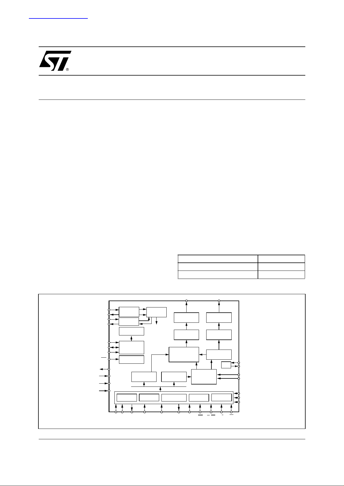
DESCRIPTION
The STE2004 is a low power CMOS LCD controller driver. Designed to drive a 65 rows by 102 columns graphic display, it provides all necessary
functions in a single chip, including on-chi p LCD
supply and bias voltages generators, resulting in a
minimum of externals compone nts and in a very
low power consumption.
STE2004 features six standard interfaces (3-lines
Serial, 3-lines SPI, 4-lines SPI, 68000 Parallel,
8080 parallel & I
2
C) for ease of interfacing with the
host micro-controller
Type Ordering Number
Bumped Wafers STE2004DIE1
Bumped Dice on Waffle Pack
STE2004DIE2
Figure 1. Block Diagram
OSC_IN
OSC_OUT
FR_IN
FR_OUT
VSENSE SLAVE
VLCD
VLCDSENSE
VSSAUX
VDD1,2
V
SS
SEL1,2
July 2003
RES
OSC
MASTER
SLAVE SYNC
BIAS VOLTAGE
GENERATOR
HIGH VOLTAGE
GENERATOR
RESET
I2C BUS
SAO SDIN/SDA_IN SDA_OUTSCLK/SCL
GENERATOR
DATA
REGISTER
9 Bit SERIAL
TIMING
CLOCK
INSTRUCTION
REGISTER
3 & 4 Line SPI
CO to C101 R0 to R64
COLUMN
DRIVERS
DATA
LATCHES
65 x 102
DRIVERS
REGISTER
SCROLL
RAM
DISPLAY
CONTROL
LOGIC
Parallel 8080
DB0
to
DB7
Parallel 68K
ROW
SHIFT
LOGIC
TEST
D/C CSSA1 SDOUT E/WR R/W- RD
TEST_MODE
TEST_VREF
ICON_MODE
EXT
SEL 0
SEL 1
SEL 2
LR0047
1/67
STE2004
PIN DESCRIPTION
N° Pad Type Function
R0 to R64 1-6
109-141
C0 to C101 6-107 O LCD Column Driver Output
SS 192-203 GND Ground pads.
V
DD1 156-163 Supply IC Positive Power Supply
V
DD2 164-171 Supply Internal Generator Supply Voltages.
V
LCD 205-209 Supply Voltage Multiplier Output
V
V
LCDSENSE
V
SENSE_SLAVE
V
SSAUX
204 Supply
145 Supply Voltage reference f or SLAVE CHARGE PUMP
190-177-
147
V
DD1AUX
142 O VDD1 Reference for Pins Configuration
SEL1,2,3 152
153
154
O LCD Row Driver Output
V oltage Multiplier Regulation Input. V
O Ground Reference for Pins Configuration
I Interface Mode Selection
- CANNOT BE LEFT FLOATING
SEL3 SEL2 SEL1 Interface
GND / VSSAUX GND / VSSAUX GND / VSSA UX
GND / VSSAUX GND / VSSAUX VDD1
GND / VSSAUX VDD1 GND / VSSAUX
GND / VSSAUX VDD1 VDD1
VDD1 GND / VSSAUX GN D / VSSAUX
VDD1 GND / VSSA UX VDD1
Sensing for Output Voltage Fine Tuning
LCDOUT
SPI 4-Lines 8 bit
SPI 3-Lines 8 bit
Serial 3-Lines 9 bit
Parallel 8080-series
Parallel 68000-series
I2C
EXT_SET 151 I Extended Instruction Set Selection
- CANNOT BE LEFT FLOATING
EXT PAD CONFIG INSTRUCTION SET SELECTED
GND or VSSAUX BASIC
VDD1 EXTENDED
ICON_MODE
155 I Extended Instruction Set Selection
- CANNOT BE LEFT FLOATING
ICON MODE PAD CONFIG ICON MODE STATUS
GND or VSSAUX DISBLED
VDD1 ENABLED
SDOUT 180 O Serial & SPI Data Output - IF UNUSED MUST BE LEFT FLOATING
SDIN - SDAIN 179 I SDIN - Serial & SPI Interface Data Input - CANNOT BE LEFT FLOATING
I
SDA IN - I
2
C Bus Data In - CANNOT BE LEFT FLOATING
SCLK - SCL 181 I SCLK - Serial & SPI Interface Clock - CANNOT BE LEFT FLOATING
I
SDA_OUT 178 O
SA0 149 I
SA1 148 I
2
C bus Clock - CANNOT BE LEFT FLOATING
SCL - I
2
C Bus Data Out IF UNUSED MUST BE LEFT FLOATING
I
2
C Slave Address BIT 0 - CANNOT BE LEFT FLOATING
I
2
C Slave Address BIT 1- CANNOT BE LEFT FLOATING
I
DB0 to DB7 182-189 I/O Paral lel Interface 8 Bi t Da ta Bus - CANNOT BE LEFT FLOATING
- RD 175 I R/W - 68000 Series Parallel Interface Read & Write Control Input
R/W
- CANNOT BE LEFT FLOATING
IRD
- 8080 Series Parallel Interface Read enable Clock Input
- CANNOT BE LEFT FLOATING
E / WR
176 I E - 68000 Series Parallel Interface Read & Write Clock Input
- CANNOT BE LEFT FLOATING
2/67
STE2004
PIN DESCRIPTION
N° Pad Type Function
E / WR 176 I WR - 8080 Series Parallel Interface - Write enable clock input
RES
D/C
CS
TEST_MODE 191 I Test Pad - 50 kohm internal Pull-down MUS T BE CO NNEC TED TO VSS/VS SAUX
TEST_VREF 146 O Test Pad - MUST B E LEF T FLOATIN G
OSCIN 144 I
OSCOUT 210 O Internal/External Oscillator Out - IF UNUSED MUST BE LEFT FLOATING
FR_OUT 211 O Master Slav e Frame Inversion Synchronization .
FR_IN 143 I Master Slave Fram e Inversi on Synchronization .
M/S 100 I Master/
(continued)
- CANNOT BE LEFT FLOATING
172 I Reset Input. Active Low.
174 I Interface Data/Command Sele ctor- CA NNOT BE LEFT FLOATING
173 I Serial & Parallel Interf aces EN AB LE. When Low the Incoming Data ar e Cl ocked In.
CANNOT BE LEFT FLOATING
Oscillator Input:
OSC_IN Configuration
High Internal Oscillator Enabled
Low Internal Oscillator Disabled
External Scillator Internal Oscillator Disabled
IF UNUSED MUST BE LEFT FLOATING
CANNOT BE LEFT FLOATING
Slave Configuration Bit:- CANNOT BE LEFT FLOATING
M/S PIN OSC_OUT FR_OUT FR_IN Charge Pump
High ENABLED Enabled Disabled AuxVsense Disabled
Low ENABLED Enabled Enabled Charge Pump in Slave Mode or Ext
Power
3/67
STE2004
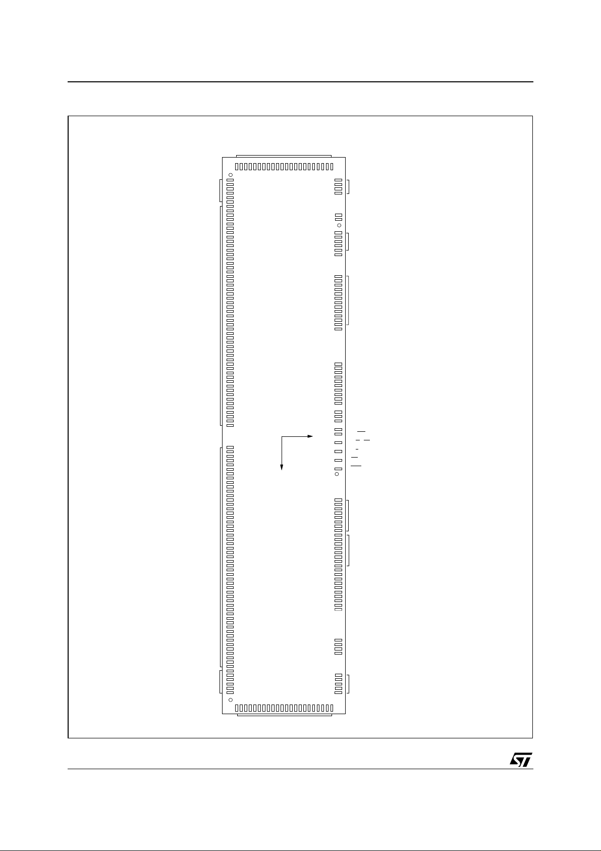
Figure 2. Chip Mechanical Drawing
ROW 5
ROW 0
COL 0
COL 50
COL 51
ROW 6
MARK_1
STE2004
(0,0)
X
ROW 27
ROW28
ROW31
FR_OUT
MARK_3
Y
MARK_4
OSC_OUT
VLCD
VLCDSENSE
VSS
TEST_MODE
VSSAUX
D0
D1
D2
D3
D4
D5
D6
D7
SCLK - SCL
SDOUT
SDIN - SDAIN
SDAOUT
VSSAUX
E - WR
R/W - RD
D/C
CS
RES
4/67
COL 101
ROW 32
ROW 37
MARK_2
ROW 38
ROW 59
VDD2
VDD1
ICON
SEL1
SEL2
SEL3
EXT_SET
M/S
SA0
SA1
VSSAUX
TEST VREF
VSENSE_SLAVE
OSC_IN
FR_IN
VDD1_AUX
ROW64/ICON
ROW63
ROW60
LR0048
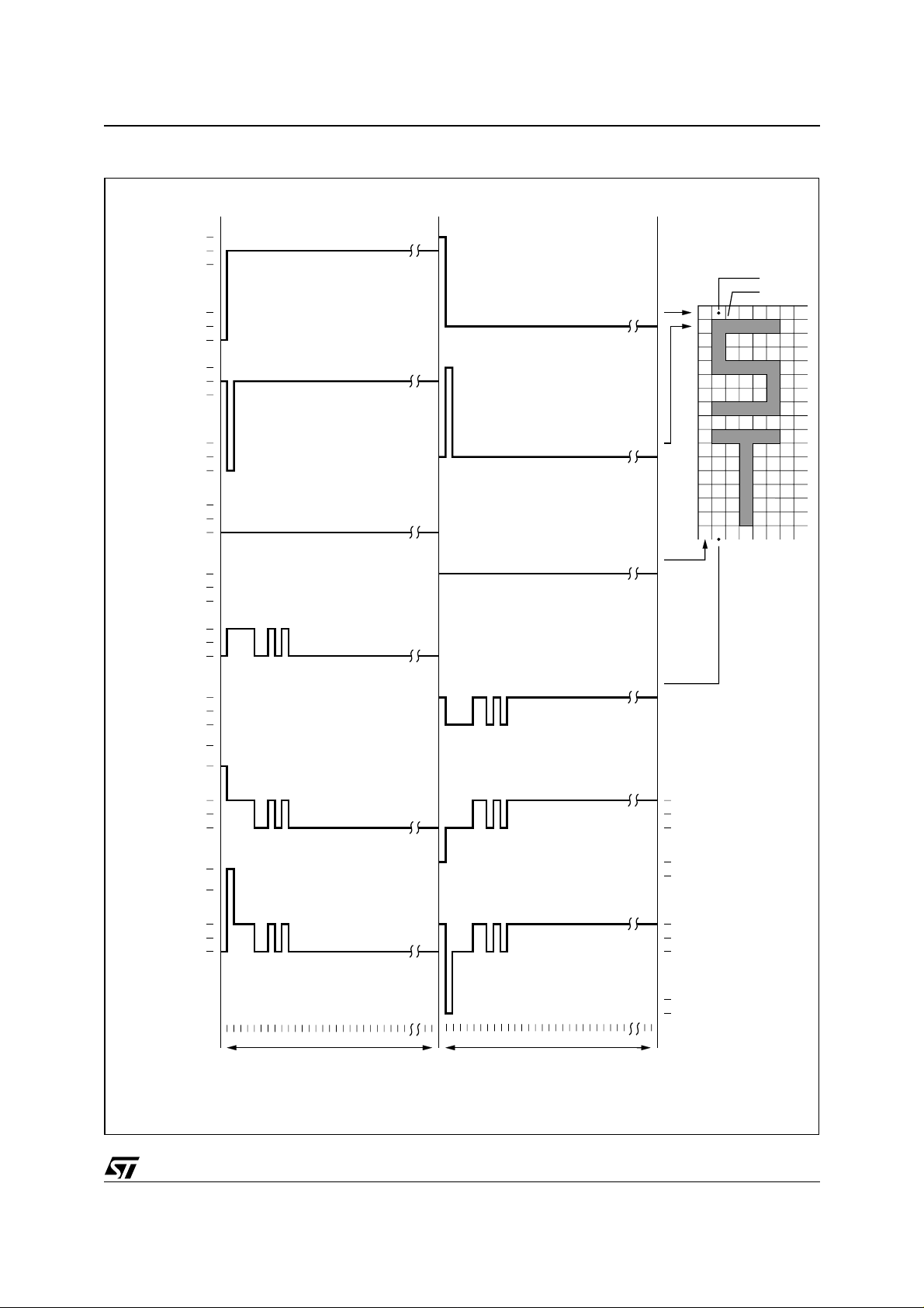
Figure 3. Improved ALTH & PLESKO Driving Method
V
LCD
V
2
V
3
ROW 0
R0 (t)
V
4
V
5
V
SS
V
LCD
V
2
V
3
ROW 1
R1 (t)
V
4
V
5
V
SS
V
LCD
V
2
V
3
COL 0
C0 (t)
V
4
V
5
V
SS
V
LCD
V
2
V
3
COL 1
C1 (t)
V
4
V
5
V
SS
V
- V
LCD
SS
V3 - V
SS
STE2004
∆V1(t)
∆V
(t)
2
V
V
state1
state2
- V
V
LCD
(t)
V3 - V
V
- V
LCD
V3 - V
- V
V
LCD
(t)
V3 - V
(t) = C1(t) - R0(t)
∆V
1
∆V
(t) = C1(t) - R1(t)
2
2
0V
SS
SS
SS
2
0V
SS
0 1 2 3 4 5 6 7 8 9 64
.......
FRAME n FRAME n + 1
0 1 2 3 4 5 6 7 8 9 64
.....
.......
.....
V
4 - V5
0V
V
SS - V5
V4 - V
VSS - V
V
4 - V5
0V
V
SS - V5
V4 - V
VSS - V
D00IN1154
LCD
LCD
LCD
LCD
5/67
STE2004
CIRCUIT DESCRIPTION
Supplies Voltages and Gro un ds
is supply voltages to the internal voltage generator (see below). If the internal voltage generator is
V
DD2
not used, this should be c onnected to V
could be different form V
DD2
.
Internal Supply Voltage Ge nerator
The IC has a fully integrated (no external capacitors required) charge pump for the Liquid Crystal Display
supply voltage generation. T he m ultiplyin g fac tor can be program m ed t o be : Aut o, X 5, X4, X3, X 2, us ing
the ’set CP Multiplication’ Command. If Auto is set, the multiplying factor is automatically selected to have
the lowest current consumption in every condition. This make possible to have an input voltage that changes over time and a constant V
CDSENSE
pad. For this voltage, eight different temperature coefficients (TC, rate of change with
voltage. The output voltage (V
LCD
temperature) can be programmed using TC1 & TC 0 or T2, T1 and T0 bits. This will ensure no contrast
degradation over the LCD operating range.
An external supply could be connected to V
such event the internal voltage generator must be programmed to zero (PRS = [0;0], Vop = 0 - Reset condition) and the Charge pump (CP[0;0]) set to 5x or Auto Mode.
Oscillator
A fully integrated oscillator (requires no externa l com ponen ts) is presen t to provi de t he clock f or t he Display System. When u sed the O SC pad must be connec ted to V
used and fed into the OSC pin.If an external oscillator is used, it must be alwa ys pres ent wh en STE2 004
is not in power down mode. An oscillator out is provided on the OSCOUT Pad to cascade two or more
drivers.
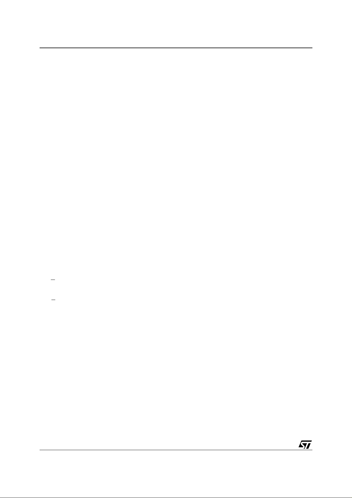
Master/Slave Mode
STE2004 support the Master Slave working Mode for Both Control Logic and Charge Pump. This function
allows to drive matrix such as 204x65 or 102x 130 using two synchronized STE2004 and the internal
Charge Pump of both device.
If M/S
is connected to VDD1, the driver is configured to work in Master Mode. When STE2004 is in Master
Mode the Vsense_Slave P in is disabled and is possib le to control the VLCD value using Vop Bits. The
Master Time Generator outputs on FR_OUT and on OSC_O UT the relevant timing referen ces.
If M/S
is connected to GND, the driver i s configured to wo rk in Slave Mode. When S TE2004 is i n Slave
Mode, the VLCD configuration set by Vop registers and the thermal compensation slope set by TC register
are neglected. The VLCD Value generated is equal to the Voltage value present on Vsense_Slave Pin so
the slave configuration can follow t he master c onfiguration. The onl y recognized configuration is Vop=0
that forces the Charge Pump to be in off state whatever is the value of Vsense_aux.
To Synchronize the Master & Slave timing circuits, the slave driver FR_IN pad must be connected to Master Driver FR_OUT pad and Slave Driver OSC_IN pad must be connected to the master driver OSC_OUT
Pad (Fig. 4). This conn ection ensu re a syn chronization at bot h Fram e level (R0 on the m aster is driven
together with the Slave R0 driver) and at Osc illator Level (sam e Frame freque ncy on the master and on
the slave). If the Synchronization at Frame level is not required, FR_IN pin must be connected toVDD1 or
to VDD1_aux (Fig. 5).
During Power Up Procesure, Master device must be forced to exit from power down before the slave device. To enter in PowerDown Mode, Slave Device must be forced in Power Down state before Master Device.
V
DD1
DD2
pad. V
2VLCD⋅
------------------------ - 200mV+≥
n4+()
to supply the LCD without using the internal generator. In
LCD
supplies the rest of the IC. V
DD1
) is tightly controlled through the V
LCD
pad. An external oscillator could be
DD1
supply voltage
DD1
L-
6/67
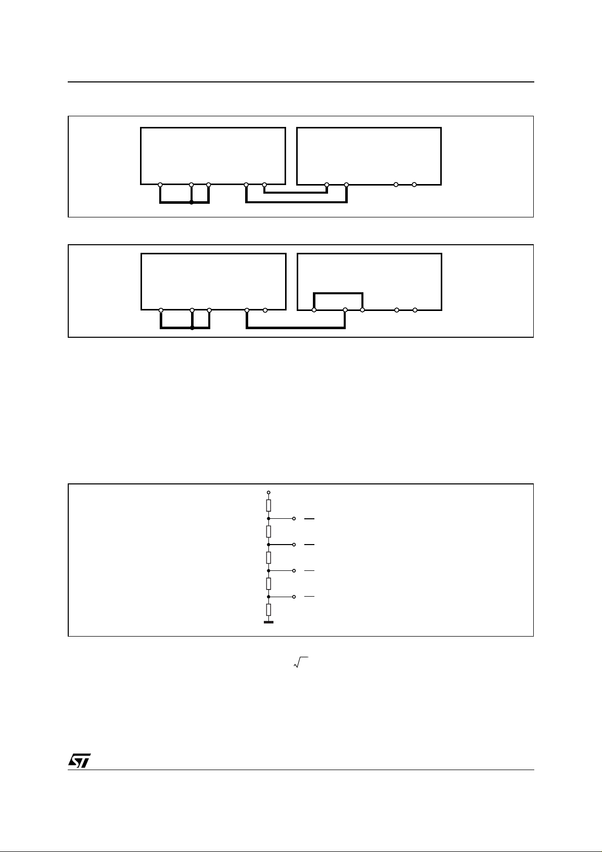
Figure 4. Master Slave Logic Connection with frame Synchronization
0
0
STE2004
STE2004
VDD1AUX
OSCOUT
FROUT OSCINFRINOSCIN FRIN
STE2004
OSCOUT FROUT
LR0219
Figure 5. Master Slave Logic Connection without frame Synchronization
STE2004
VDD1AUX
OSCOUT
FROUTOSCIN FRIN
VDD1AUX
STE2004
OSCIN
OSCOUT FROUT
FRIN
LR022
Bias Levels
To properly drive the LCD, six (Including VLCD and VSS) different voltage (Bias ) levels are generated.
The ratios among these levels and VLCD, s hould be selected acc ording to the MUX ratio (m). They are
established to be (Fig. 6):
V
LCD
n3+
------------ -
,
n4+
V
LCD
n2+
------------ -
,
n4+
V
LCD
2
------------ -
,
n4+
V
LCD
------------ -
,
n4+
1
V
LCD,VSS
Figure 6. Bias level Generator
V
R
R
nR
R
R
LCD
n + 3
n + 4
n + 2
n + 4
n + 4
n + 4
V
2
1
SS
·V
LCD
·V
LCD
·V
LCD
·V
LCD
D00IN115
thus providing an 1/(n+4) ratio, with n calculated from:
nm3–=
For m = 65, n = 5 and an 1/9 ratio is set.
For m = 49, n =4 and an 1/8 ratio is set.
The STE2004 provides three bits (BS0, BS1, BS2) for programming the desired Bias Ratio as shown below:
7/67
STE2004
BS2 BS1 BS0 n
0007
0016
0105
0114
1003
1012
1101
1110
The following table Bias Level for m = 65 and m = 49 are provided:
Symbol m = 65 (1/9) m = 49 (1/8)
V1 V
V2 8/9*V
V3 7/9*V
V4 2/9*V V
V5 1/9 *V
V6 V
LCD
LCD
LCD
LCD
LCD
SS
V
7/8*V
6/8*V
2/8*V
1/8*V
V
LCD
LCD
LCD
LCD
LCD
SS
LCD Voltage Generation
The LCD Voltage at reference temperature (To = 27°C) can be set using the VOP register content according to
the following formula:
V
(T=To) = V
LCD
o = (Ai+VOP · B) (i=0,1,2)
LCD
with the following values:
Symbol Value Unit Note
Ao 2.95 V PRS = [0;0]
A1 6.83 V PRS = [0;1]
A2 10.71 V PRS = [1;0]
B 0.03 03 V
To 27 °C
Note that the three PRS values produce three adjacent ranges for VLCD. If the VOP register and PRS bits
are set to zero the internal voltage generator is switched off.
The proper value for the VLCD is a function of the Liquid Crystal Threshold Voltage (Vth) and of the Multiplexing Rate. A general expression for this is:
1m+
For MUX Rate m = 65 the ideal V
LCD
V
is:
LCD
----------------------------------- -
21
V
LCD(to)
⋅
= 6.85 · V
-------- -–
1
m
th
V
⋅=
th
than:
6.85 VthAi–⋅()
op
-----------------------------------------=
0.03
V
8/67
STE2004
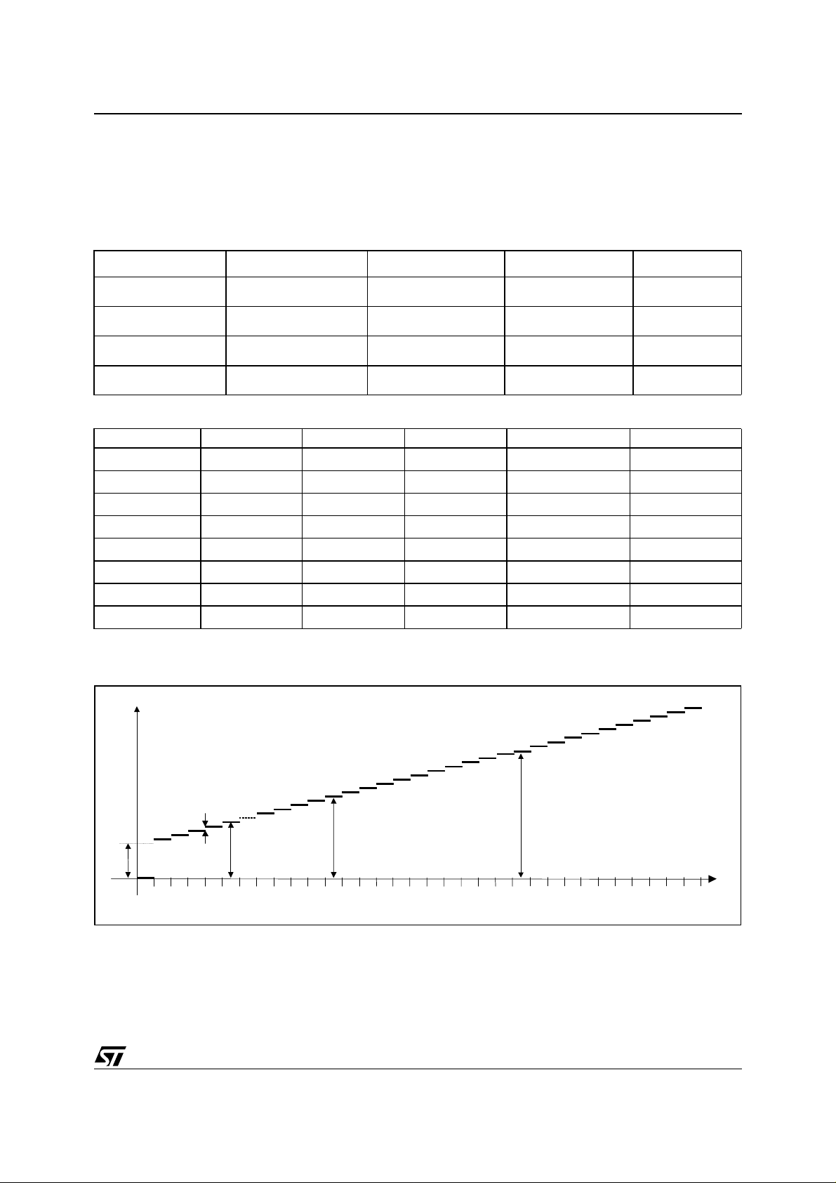
Temperature Coefficients
As the viscosity, and therefore the contrast, of the LCD are subject to change with temperature, there's
the need to vary the LCD Voltage with temperature. STE2004 provides the possibility to change the VLCD
in a linear fashion against temperature with eight different Temperature Coefficient selectable through T2,
T1 and T0 bits. Only four of them are available through basic instruction set.
NAME TC1 TC0 Value Unit
TC0 0 0
TC2 0 1
TC3 1 0
TC6 1 1
-0.7 · 10
-1.05· 10
-2.1 · 10
-0.0· 10
-3
-3
-3
-3
NAME T2 T1 T0 Value Unit
TC0 0 0 0
TC1 0 1 1
TC2 1 0 0
TC3 1 1 1
TC4 1 1 1
TC5 1 1 1
TC6 1 1 1
TC7 1 1 1
-0.35 · 10
-0.7 · 10
-1.05· 10
-1.4 · 10
-1.75· 10
-2.1 · 10
-0.0· 10
-2.3· 10
-3
-3
-3
-3
-3
-3
-3
-3
Figure 7.
1/ °C
1/°C
1/°C
1/°C
1/ °C
1/°C
1/°C
1/°C
1/°C
1/°C
1/°C
1/°C
LCD
V
1
A
00h 01h 02h 03h 04h 05h ….
Finally, the V
B
1
0
A
+ B
7Ch 7Dh 7Eh
PRS = [0;0]
voltage at a given (T) temperature can be calculated as:
LCD
A
7Fh 00h 01h 02h
(T) = V
V
LCD
03h 04h
05h …. 7Ch
PRS = [0;1]
o · [1 + (T-To) · TC]
LCD
7Dh 7Eh 7Fh
2
A
00h 01h 02h 03h 04h
05h 7Ch
….
PRS = [1;0]
7Dh 7Eh 7Fh
O
V
9/67

STE2004
Display Data RAM
The STE2004, provides an 102X65 bits Static RAM to store Display data. This is organized into 9 (Bank0
to Bank8) banks with 102 Bytes. One of these Banks can be used for Icons. RAM access is accomplished
in either one of the Bus Interfaces provid ed (s ee be low). A llowed addres ses are X 0 to X101 (Horizontal)
and Y0 to Y8 (Vertical).
When writing to RAM, four addressing mode are provided:
• Normal Horizontal (MX=0 and V=0), having the column with address X= 0 located on the left of the memory map. The X pointer is increased after each byte written. After the last column address (X=X-Carriage), Y address pointer is set to jump to the following bank and X restarts from X=0. (Fig. 8)
• Normal Vertical (MX=0 and V=1), having the column with address X= 0 located on the left of the memory
map. The Y pointer is increased after each byte written. After th e l ast Y b ank address (Y=Y-Carriage),
X address pointer is set to jump to next column and Y restarts from Y=0 (Fig. 9).
• Mirrored Horizontal (MX=1 and V=0), having the column with address X= 0 located on the right of the
memory map. The X pointer is increased af ter each byte written. After the last column address (X=XCarriage), Y address pointer is set to jump to the next bank and X restarts from X=0 (fig. 10).
• Mirrored Vertical (MX=1 and V=1), having the column with address X= 0 located on the right of the memory map. The Y pointer is increased after each byte written. After the last Y bank address (Y=Y-Carriage), the X pointer is set to jump to next column and Y restarts from Y=0 (fig. 11).
After the last allowed address (X;Y)=(X-Carriage; Y-Carriage), the address pointers always jump to the
cel l with addre ss (X;Y) = (0;0) (Fig. 12,13,14 & 15).
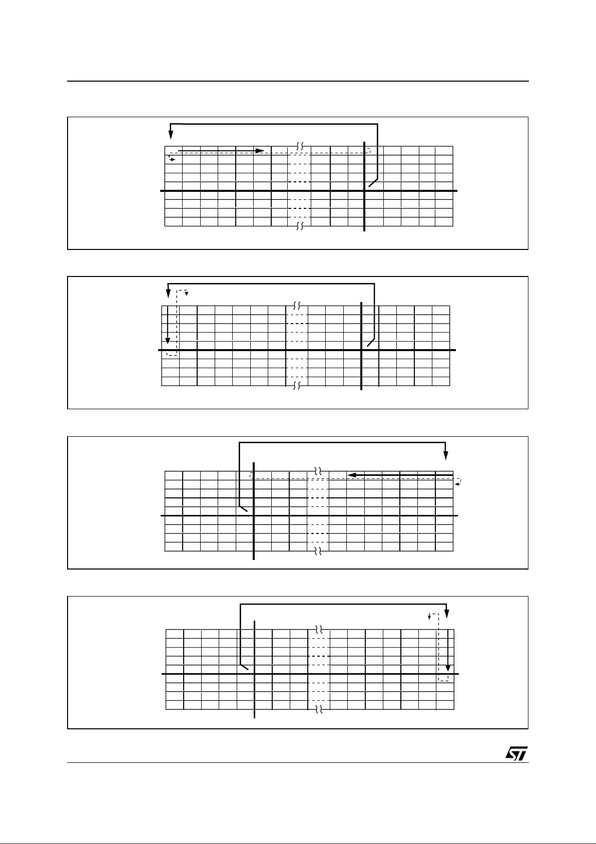
Data bytes in the memory could have the MSB either on top (D0 = 0, Fig.16) or on the bottom (D0=1, Fig.
17).
The STE2004 provides also means to alter the normal output addressing. A mirroring of the Display along
the X axis is enabled setting t o a l ogic one MY bit.This function does n't af fect t he cont ent of the me mory
map. It is only related to the memory read process.
When ICON MODE=1 the Icon Row is not mirrored with MY and is not scrolled.
When ICON MODE=0 the Icon Row is like an other graphic line and is mirrored and scrolled.
Three are the multiplex ratio available when the partial display mode i s disabled (MUX 33, MU X 49 and
MUX 65). Only a subset of writable rows are output on Row drivers in MUX 33,49 & 65 Mode.
When Y-Carriage<M U X/ 8, if Mux 49 is selected only the first 49 m emory rows are v isualized; if Mux 33 i s
selected only the first 33 memo ry rows are v isualized. Th e unused output row & colum n drivers m ust be
left floating.
When Y-Carri ag e<=MUX/8 the icon Bank is locat ed to BANK 8 i n MUX 65 Mode, to BANK6 in MUX 49
Mode and to BANK 4 in MUX 33 Mode.
In Mux 33 & 49 Mode, when Y-Carriage>MUX/8 lines only 33, 49 lines are visualized.
It is possible to select whic h l ines of DDRAM are c onnected on the output dri vers using the scrolling func-
tion (Range: 0-Y-Carriage*8). When Y-Carriage>MUX/8 lines, the icon row is moved in DDRAM to the
first row of the Bank correspondant to Y-CARRIAGE Return value, being always connected on the same
output Driver.
When MY=0, the icon Row is output on R64 in mux 65 mode, on R56 in MUX 49 and on R48 in MUX33.
When MY=1, and ICON MODE=0, the icon Row is output on R0 whatever is the MUX Rate.
10/67
STE2004
2
Figure 8. Auto m at ic da ta RAM wri t in g sequence with V=0 and Data RAM N or m a l Form a t ( MX =0)1
BANK 0
BANK 1
BANK 2
BANK 3
BANK 4
BANK 5
BANK 6
BANK 7
BANK 8
0123 9899100101
LR0049
Figure 9. Auto m at ic da ta RAM wri t in g sequence with V=1 and Data RAM N or m a l Form a t ( MX =0)
BANK 0
BANK 1
BANK 2
BANK 3
BANK 4
BANK 5
BANK 6
BANK 7
BANK 8
010123 9899100101
LR0050
Figure 10. Automatic data RAM writing sequence with V=0 and Data RAM Mirrored Format (MX=1)
1
1
BANK 0
BANK 1
BANK 2
BANK 3
BANK 4
BANK 5
BANK 6
BANK 7
BANK 8
32109899100101
LR0051
Figure 11. Automatic data RAM writing sequence with V=1 and Data RAM Mirrored Format (MX=1)1
BANK 0
BANK 1
BANK 2
BANK 3
BANK 4
BANK 5
BANK 6
BANK 7
BANK 8
1. X Carriage=101; Y-Carriage = 8
10329899100101
LR005
11/67
STE2004
3
4
6
Figure 12. Automatic data RAM writing sequence with X-Y Carriage Return (V=0; MX=0)
BANK 0
BANK 1
BANK 2
Y CARR
BANK 7
BANK 8
0123
X CARR
98 99 100 101
LR005
Figure 13. Automatic data RAM writing sequence with X-Y Carriage Return (V=1; MX=0)
0123
X CARR
BANK 0
BANK 1
BANK 2
Y CARR
BANK 7
BANK 8
98 99 100 101
LR005
Figure 14. Automatic data RAM writing sequence with X-Y Carriage Return (V=0; MX=1)
X CARR
BANK 0
BANK 1
BANK 2
Y CARR
BANK 7
BANK 8
1239899100101
0
LR0055
Figure 15. Automatic data RAM writing sequence with X-Y Carriage Return (V=1; MX=1)
X CARR
9899100101
BANK 0
BANK 1
BANK 2
Y CARR
BANK 7
BANK 8
0
123
LR005
12/67
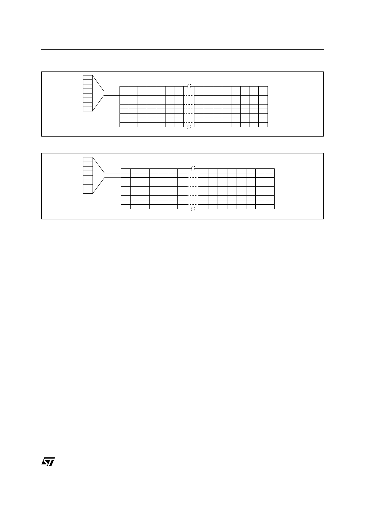
Figure 16. Data RA M Byte or ga n iza ti on with D0 = 0
8
MSB
0
1 2 3 98 99 100 101
LSB
BANK 0
BANK 1
BANK 2
BANK 3
BANK 4
BANK 5
BANK 6
BANK 7
BANK 8
Figure 17. Data RA M Byte or ga n iza ti on with D0 = 1
LSB
0123 9899100101
MSB
BANK 0
BANK 1
BANK 2
BANK 3
BANK 4
BANK 5
BANK 6
BANK 7
BANK 8
STE2004
LR0057
LR005
13/67
STE2004
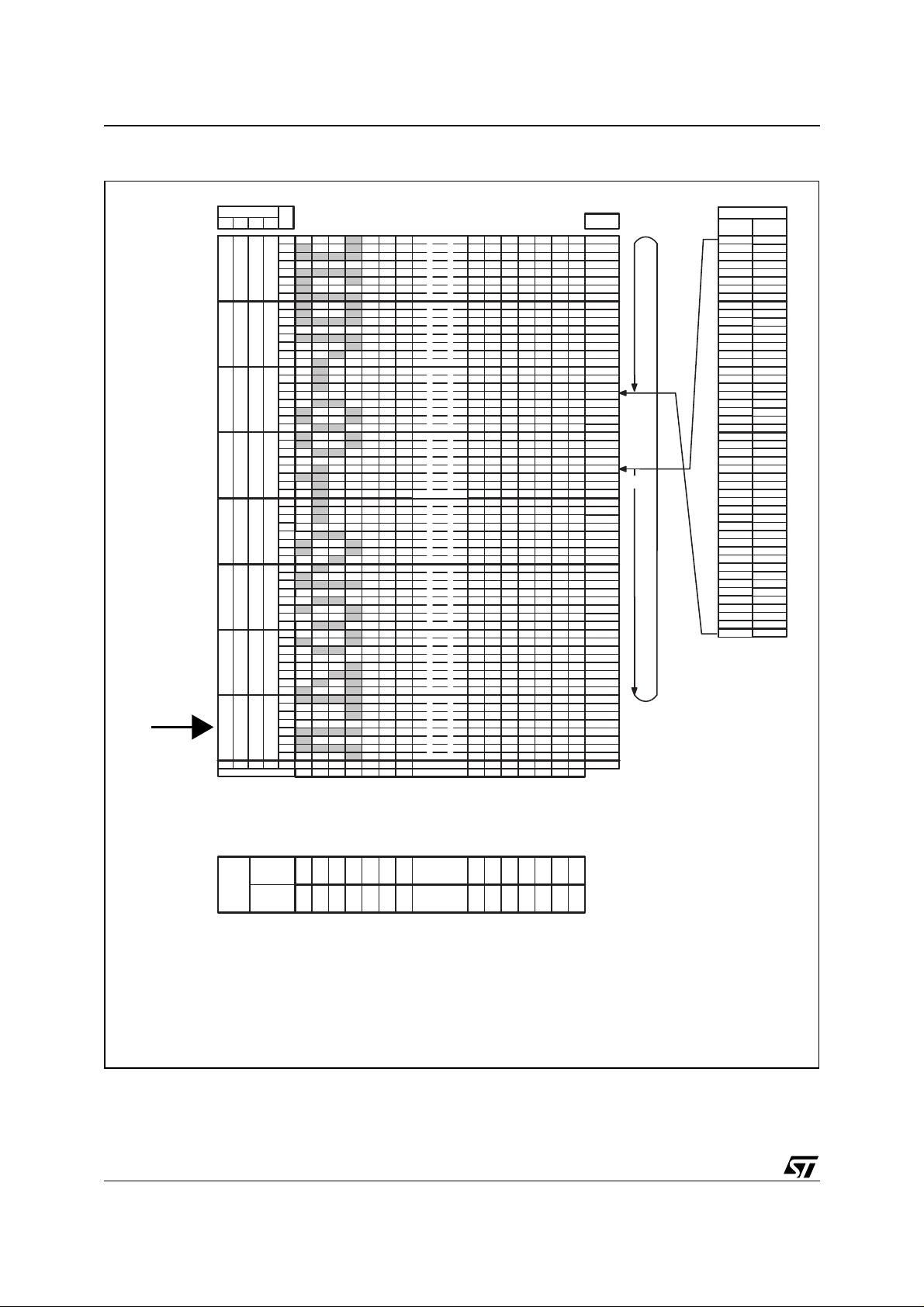
Figure 18. Memory Rows vs. Row Drivers Mapping ICON_MODE=1 and MUX 65
Y-CARRIAGE
Y Address
D3
D2 D1 D0
0
0
0
0
0
0
0
0
1
X address
D
a
t
a
D0
D1
D2
D3
0
0
0
D4
D5
D6
D7
D0
D1
D2
D3
0
1
0
D4
D5
D6
D7
D0
D1
D2
D3
1
0
0
D4
D5
D6
D7
D0
D1
D2
D3
1
1
0
D4
D5
D6
D7
D0
D1
D2
D3
0
0
1
D4
D5
D6
D7
D0
D1
D2
D3
0
1
1
D4
D5
D6
D7
D0
D1
D2
D3
1
0
1
D4
D5
D6
D7
D0
D1
D2
D3
1
1
1
D4
D5
D6
D7
0
0
0
D0
00H
02H 06H03H 04H 05H
01H
Page 0
Page 1
Page 2
Page 3
Page 4
Page 5
Page 6
Page 7
Page 8
5FH
61H 65H62H 63H 64H
60H
Line
Address
00H
01H
02H
03H
04H
05H
06H
07H
08H
09H
0AH
0BH
0CH
0DH
0EH
0FH
10H
11H
12H
13H
14H
15H
16H
17H
18H
19H
1AH
1BH
1CH
1DH
1EH
1FH
20H
21H
22H
23H
24H
25H
26H
27H
28H
29H
2AH
2BH
2CH
2DH
2EH
2FH
30H
31H
32H
33H
34H
35H
36H
37H
38H
39H
3AH
3BH
3CH
3DH
3EH
3FH
Scrolling Pointer
ROW Output
Normal
Reverse
direction
direction
R0
R1
R2
R3
R4
R5
R6
R7
R8
R9
R10
R11
R12
R13
R14
R15
R16
R17
R18
R19
R20
R21
R22
R23
R24
R25
R26
R27
R28
R29
R30
R31
R32
R33
R34
R35
R36
R37
R38
R39
R40
R41
R42
R43
R44
R45
R46
R47
R48
R49
R50
R51
R52
R53
R54
R55
R56
R57
R58
R59
R60
R61
R62
R63
R64 R64
R63
R62
R61
R60
R59
R58
R57
R56
R55
R54
R53
R52
R51
R50
R49
R48
R47
R46
R45
R44
R43
R42
R41
R40
R39
R38
R37
R36
R35
R34
R33
R32
R31
R30
R29
R28
R27
R26
R25
R24
R23
R22
R21
R20
R19
R18
R17
R16
R15
R14
R13
R12
R11
R10
R9
R8
R7
R6
R5
R4
R3
R2
R1
R0
lr0268
14/67
COL
Output
C
C
O
L
C
O
L
100 99
C
O
O
L
L
C
C
O
O
L
L
98 979695
C
O
L
C
O
L
C
Normal
O
L
Direction
0 1011 2 3 4 5 6 1009998979695
C
Reverse
O
L
Direction
101
C
C
C
C
O
O
L
L
C
C
O
O
L
L
C
C
C
O
L
C
O
L
6
C
O
O
O
L
L
L
C
C
C
O
O
O
L
L
L
4
5
C
O
O
O
L
L
L
C
C
C
O
O
O
L
L
L
0
123
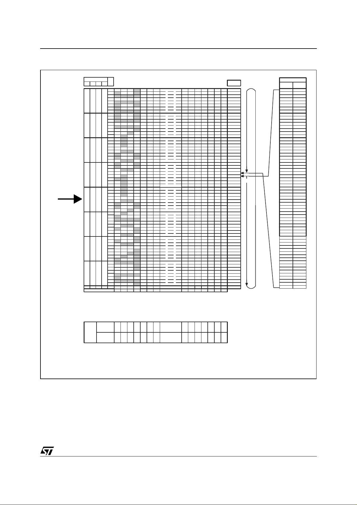
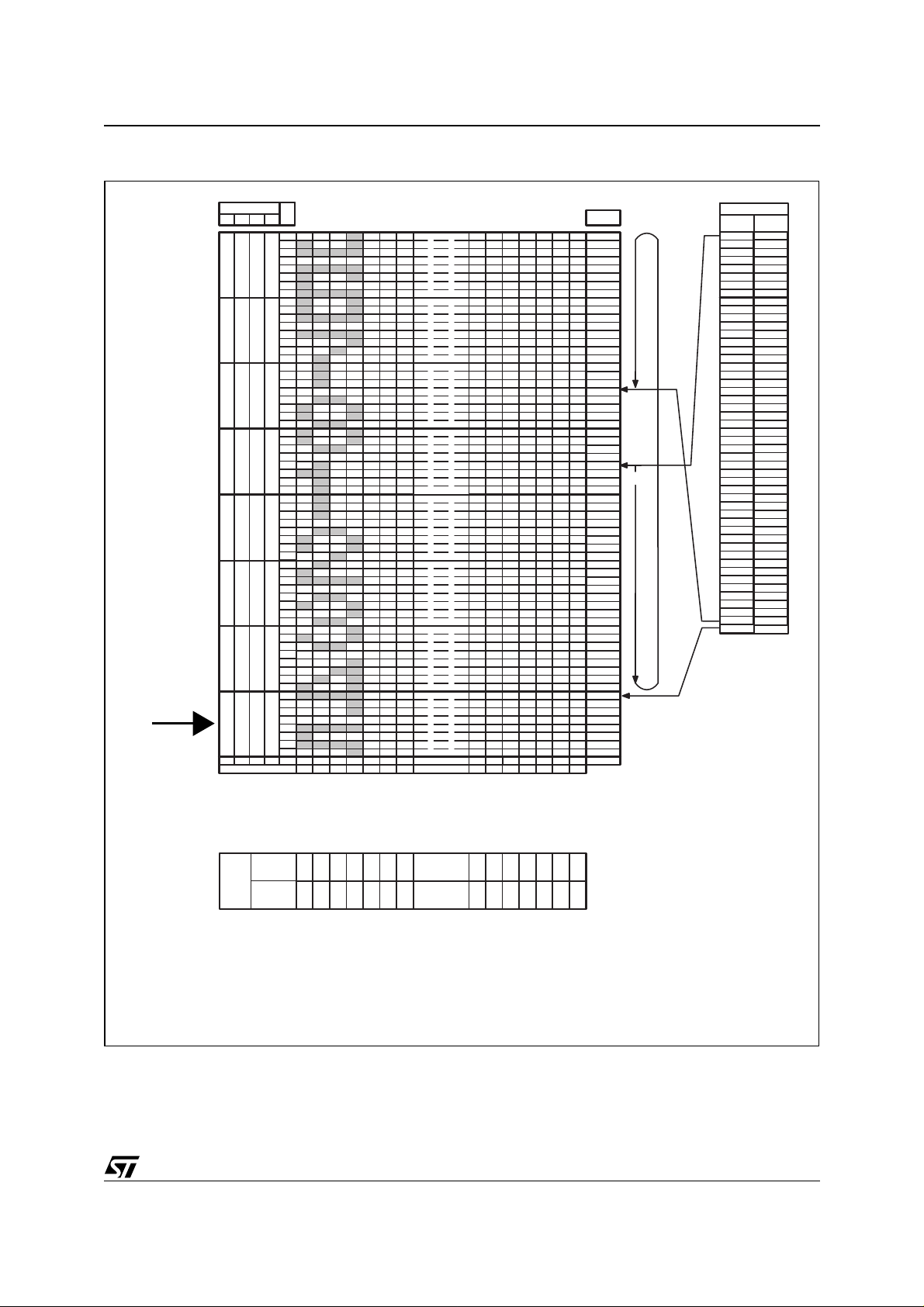
Figure 19. Memory Rows vs. Row Drivers Mapping ICON_MODE=0 and MUX 65
STE2004
Y-CARRIAGE
Y Address
D3
D2 D1 D0
0
0
0
0
0
0
0
0
0
1
0
1
0
1
0
1
0
1
X address
D
a
t
a
D0
D1
D2
D3
0
0
D4
D5
D6
D7
D0
D1
D2
D3
0
1
D4
D5
D6
D7
D0
D1
D2
D3
1
0
D4
D5
D6
D7
D0
D1
D2
D3
1
1
D4
D5
D6
D7
D0
D1
D2
D3
0
0
D4
D5
D6
D7
D0
D1
D2
D3
0
1
D4
D5
D6
D7
D0
D1
D2
D3
1
0
D4
D5
D6
D7
D0
D1
D2
D3
1
1
D4
D5
D6
D7
0
0
D0
00H
02H 06H03H 04H 05H
01H
Page 0
Page 1
Page 2
Page 3
Page 4
Page 5
Page 6
Page 7
Page 8
5FH
61H 65H62H 63H 64H
60H
Line
Address
00H
01H
02H
03H
04H
05H
06H
07H
08H
09H
0AH
0BH
0CH
0DH
0EH
0FH
10H
11H
12H
13H
14H
15H
16H
17H
18H
19H
1AH
1BH
1CH
1DH
1EH
1FH
20H
21H
22H
23H
24H
25H
26H
27H
28H
29H
2AH
2BH
2CH
2DH
2EH
2FH
30H
31H
32H
33H
34H
35H
36H
37H
38H
39H
3AH
3BH
3CH
3DH
3EH
3FH
40H
Scrolling Pointer
ROW Output
Normal
direction
R0
R1
R2
R3
R4
R5
R6
R7
R8
R9
R10
R11
R12
R13
R14
R15
R16
R17
R18
R19
R20
R21
R22
R23
R24
R25
R26
R27
R28
R29
R30
R31
R32
R33
R34
R35
R36
R37
R38
R39
R40
R41
R42
R43
R44
R45
R46
R47
R48
R49
R50
R51
R52
R53
R54
R55
R56
R57
R58
R59
R60
R61
R62
R63
R64
Reverse
direction
R64
R63
R62
R61
R60
R59
R58
R57
R56
R55
R54
R53
R52
R51
R50
R49
R48
R47
R46
R45
R44
R43
R42
R41
R40
R39
R38
R37
R36
R35
R34
R33
R32
R31
R30
R29
R28
R27
R26
R25
R24
R23
R22
R21
R20
R19
R18
R17
R16
R15
R14
R13
R12
R11
R10
R9
R8
R7
R6
R5
R4
R3
R2
R1
R0
COL
Output
Normal
Direction
Reverse
Direction
C
C
C
C
O
L
C
O
L
100 99
C
O
O
L
L
C
C
O
O
L
L
98 979695
C
O
L
0
C
O
L
101
C
C
C
O
O
O
L
L
L
C
C
C
O
O
O
L
L
L
C
C
C
O
L
C
O
L
6
C
O
O
O
L
L
L
C
C
C
O
O
O
L
L
L
4
5
C
O
O
O
L
L
L
1011 2 3 4 5 6 1009998979695
C
C
C
O
O
O
L
L
L
0
123
lr0269
15/67
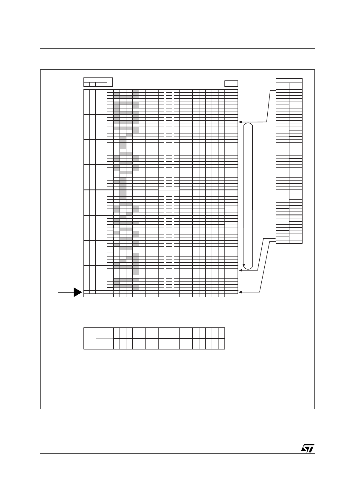
STE2004
Figure 20. Memory Rows vs. Row Drivers Mapping ICON_MODE=1,
D
a
t
a
D0
D1
D2
D3
0
0
0
D4
D5
D6
D7
D0
D1
D2
D3
0
1
0
D4
D5
D6
D7
D0
D1
D2
D3
1
0
0
D4
D5
D6
D7
D0
D1
D2
D3
1
1
0
D4
D5
D6
D7
D0
D1
D2
D3
0
0
1
D4
D5
D6
D7
D0
D1
D2
D3
0
1
1
D4
D5
D6
D7
D0
D1
D2
D3
1
0
1
D4
D5
D6
D7
D0
D1
D2
D3
1
1
1
D4
D5
D6
D7
0
0
0
D0
00H
02H 06H03H 04H 05H
01H
Page 0
Page 1
Page 2
Page 3
Page 4
Page 5
Page 6
Page 7
Page 8
5FH
60H
61H 65H62H 63H 64H
Y-CARRIAGE
Y Address
D3
D2 D1 D0
0
0
0
0
0
0
0
0
1
X address
Y-Carriage<=6
Line
Address
00H
01H
02H
03H
04H
05H
06H
07H
08H
09H
0AH
0BH
0CH
0DH
0EH
0FH
10H
11H
12H
13H
14H
15H
16H
17H
18H
19H
1AH
1BH
1CH
1DH
1EH
1FH
20H
21H
22H
23H
24H
25H
26H
27H
28H
29H
2AH
2BH
2CH
2DH
2EH
2FH
30H
31H
32H
33H
34H
35H
36H
37H
38H
39H
3AH
3BH
3CH
3DH
3EH
3FH
and MUX 49
Scrolling Pointer
ROW Output
Normal
direction
R0
R1
R2
R3
R4
R5
R6
R7
R8
R9
R10
R11
R12
R13
R14
R15
R16
R17
R18
R19
R20
R21
R22
R23
R32
R33
R34
R35
R36
R37
R38
R39
R40
R41
R42
R43
R44
R45
R46
R47
R48
R49
R50
R51
R52
R53
R54
R55
R56
Reverse
direction
R55
R54
R53
R52
R51
R50
R49
R48
R47
R46
R45
R44
R43
R42
R41
R40
R39
R38
R37
R36
R35
R34
R33
R32
R23
R22
R21
R20
R19
R18
R17
R16
R15
R14
R13
R12
R11
R10
R9
R8
R7
R6
R5
R4
R3
R2
R1
R0
R56
16/67
COL
Output
Normal
Direction
Reverse
Direction
C
C
C
C
O
L
C
O
L
100 99
C
O
O
L
L
C
C
O
O
L
L
98 979695
C
O
L
0
C
O
L
101
C
C
C
O
O
O
L
L
L
C
C
C
O
O
O
L
L
L
C
C
C
O
L
C
O
L
6
C
O
O
O
L
L
L
C
C
C
O
O
O
L
L
L
4
5
C
O
O
O
L
L
L
1011 2 3 4 5 6 1009998979695
C
C
C
O
O
O
L
L
L
0
123
lr0270
STE2004
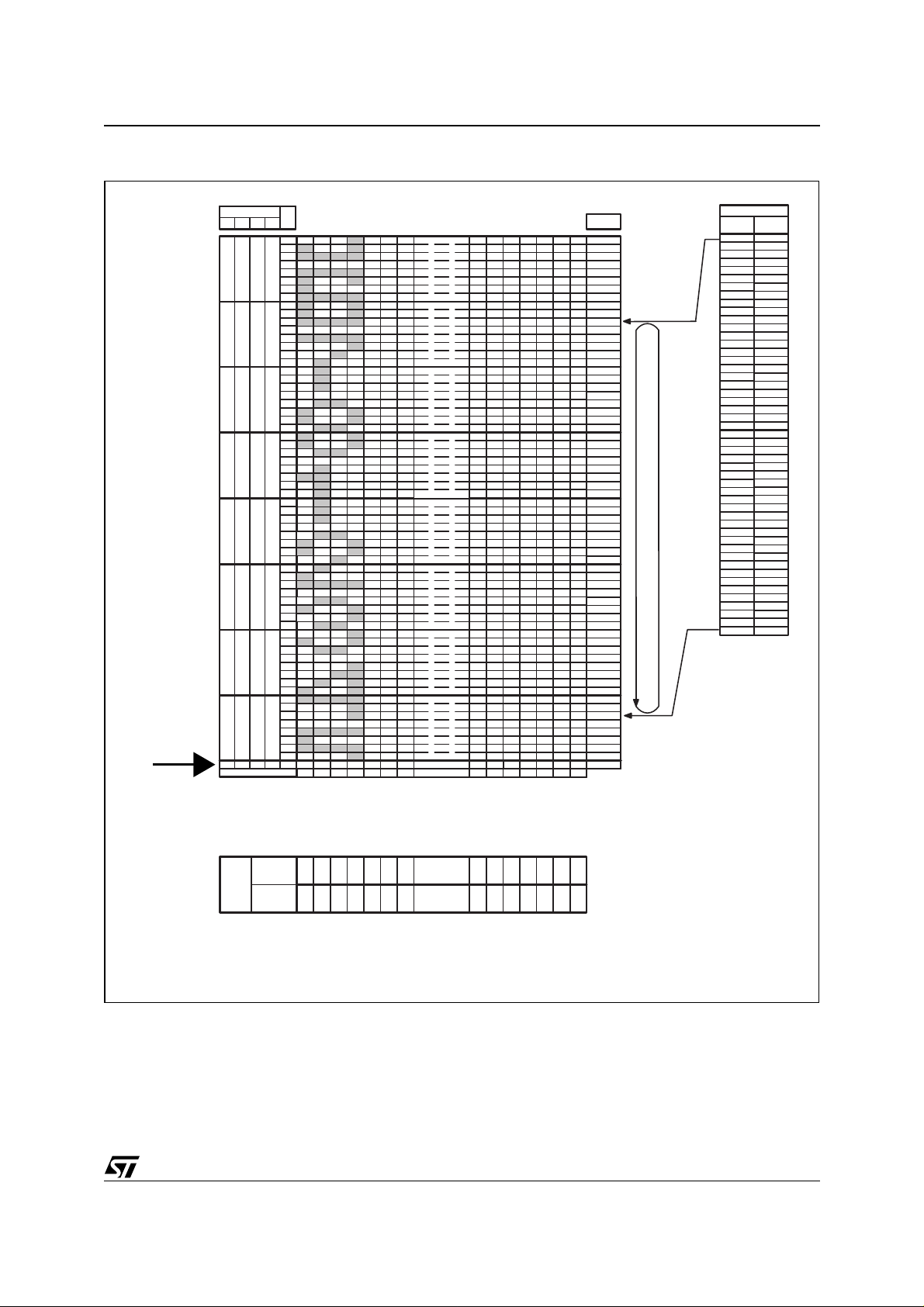
Figure 21. Memory Rows vs. Row Drivers Mapping ICON_MODE=0,
D2 D1 D0
0
0
0
0
1
0
1
0
0
1
0
1
1
1
1
1
0
0
D
a
t
a
D0
D1
D2
D3
0
D4
D5
D6
D7
D0
D1
D2
D3
1
D4
D5
D6
D7
D0
D1
D2
D3
0
D4
D5
D6
D7
D0
D1
D2
D3
1
D4
D5
D6
D7
D0
D1
D2
D3
0
D4
D5
D6
D7
D0
D1
D2
D3
1
D4
D5
D6
D7
D0
D1
D2
D3
0
D4
D5
D6
D7
D0
D1
D2
D3
1
D4
D5
D6
D7
0
D0
00H
02H 06H03H 04H 05H
01H
Page 0
Page 1
Page 2
Page 3
Page 4
Page 5
Page 6
Page 7
Page 8
5FH
60H
Y-CARRIAGE
Y Address
D3
0
0
0
0
0
0
0
0
1
X address
Y-Carriage<=6
61H 65H62H 63H 64H
and MUX 49
Line
Address
00H
01H
02H
03H
04H
05H
06H
07H
08H
09H
0AH
0BH
0CH
0DH
0EH
0FH
10H
11H
12H
13H
14H
15H
16H
17H
18H
19H
1AH
1BH
1CH
1DH
Scrolling Pointer
1EH
1FH
20H
21H
22H
23H
24H
25H
26H
27H
28H
29H
2AH
2BH
2CH
2DH
2EH
2FH
30H
31H
32H
33H
34H
35H
36H
37H
38H
39H
3AH
3BH
3CH
3DH
3EH
3FH
ROW Output
Normal
direction
R0
R1
R2
R3
R4
R5
R6
R7
R8
R9
R10
R11
R12
R13
R14
R15
R16
R17
R18
R19
R20
R21
R22
R23
R32
R33
R34
R35
R36
R37
R38
R39
R40
R41
R42
R43
R44
R45
R46
R47
R48
R49
R50
R51
R52
R53
R54
R55
R56
Reverse
direction
R56
R55
R54
R53
R52
R51
R50
R49
R48
R47
R46
R45
R44
R43
R42
R41
R40
R39
R38
R37
R36
R35
R34
R33
R32
R23
R22
R21
R20
R19
R18
R17
R16
R15
R14
R13
R12
R11
R10
R9
R8
R7
R6
R5
R4
R3
R2
R1
R0
COL
Output
Normal
Direction
Reverse
Direction
C
C
C
C
O
L
C
O
L
100 99
C
O
O
L
L
C
C
O
O
L
L
98 979695
C
O
L
0
C
O
L
101
C
C
C
O
O
O
L
L
L
C
C
C
O
O
O
L
L
L
C
C
C
O
L
C
O
L
6
C
O
O
O
L
L
L
C
C
C
O
O
O
L
L
L
4
5
C
O
O
O
L
L
L
1011 2 3 4 5 6 1009998979695
C
C
C
O
O
O
L
L
L
0
123
lr0271
17/67
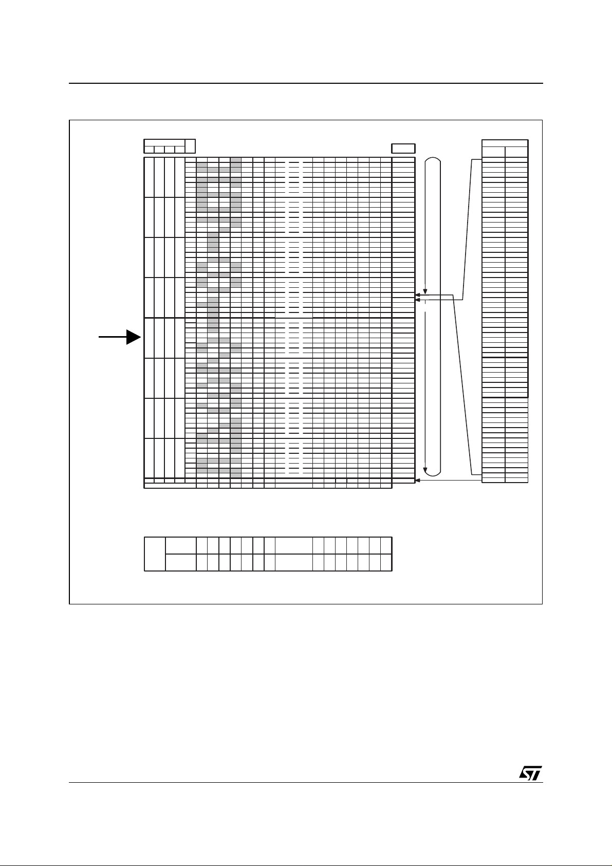
STE2004
Figure 22.
Y-CARRIAGE
Memory Rows vs. Row Drivers Mapping ICON_MODE=0, Y-Carriage=7, Scrolling Pointer>07h and MUX 49
Y Address
D3
D2 D1 D0
0
0
0
0
0
0
0
0
1
X address
D
a
t
a
D0
D1
D2
D3
0
0
0
D4
D5
D6
D7
D0
D1
D2
D3
0
1
0
D4
D5
D6
D7
D0
D1
D2
D3
1
0
0
D4
D5
D6
D7
D0
D1
D2
D3
1
1
0
D4
D5
D6
D7
D0
D1
D2
D3
0
0
1
D4
D5
D6
D7
D0
D1
D2
D3
0
1
1
D4
D5
D6
D7
D0
D1
D2
D3
1
0
1
D4
D5
D6
D7
D0
D1
D2
D3
1
1
1
D4
D5
D6
D7
0
0
0
D0
00H
02H 06H03H 04H 05H
01H
Page 0
Page 1
Page 2
Page 3
Page 4
Page 5
Page 6
Page 7
Page 8
5FH
60H
61H 65H62H 63H 64H
Line
Address
00H
01H
02H
03H
04H
05H
06H
07H
08H
09H
0AH
0BH
0CH
0DH
0EH
0FH
10H
11H
12H
13H
14H
15H
16H
17H
18H
19H
1AH
1BH
1CH
1DH
1EH
1FH
20H
21H
22H
23H
24H
25H
26H
27H
28H
29H
2AH
2BH
2CH
2DH
2EH
2FH
30H
31H
32H
33H
34H
35H
36H
37H
38H
39H
3AH
3BH
3CH
3DH
3EH
3FH
Scrolling Pointer
ROW Output
Normal
direction
R0
R1
R2
R3
R4
R5
R6
R7
R8
R9
R10
R11
R12
R13
R14
R15
R16
R17
R18
R19
R20
R21
R22
R23
R32
R33
R34
R35
R36
R37
R38
R39
R40
R41
R42
R43
R44
R45
R46
R47
R48
R49
R50
R51
R52
R53
R54
R55
R56
Reverse
direction
R56
R55
R54
R53
R52
R51
R50
R49
R48
R47
R46
R45
R44
R43
R42
R41
R40
R39
R38
R37
R36
R35
R34
R33
R32
R23
R22
R21
R20
R19
R18
R17
R16
R15
R14
R13
R12
R11
R10
R9
R8
R7
R6
R5
R4
R3
R2
R1
R0
18/67
COL
Output
Normal
Direction
Reverse
Direction
101
C
C
C
C
O
L
C
O
L
100 99
C
O
O
L
L
C
C
O
O
L
L
98 979695
C
O
L
0
C
O
L
C
C
C
O
O
O
L
L
L
C
C
C
O
O
O
L
L
L
C
C
C
O
L
C
O
L
6
C
O
O
O
L
L
L
C
C
C
O
O
O
L
L
L
4
5
C
O
O
O
L
L
L
1011 2 3 4 5 6 1009998979695
C
C
C
O
O
O
L
L
L
0
123
lr0275
STE2004
Figure 23.
Y-CARRIAGE
Memory Rows vs. Row Drivers Mapping ICON_MODE=1, Y-Carriage=7, Scrolling Pointer>07h and MUX 49
Y Address
D3
D2 D1 D0
0
0
0
0
0
0
0
0
1
X address
D
a
t
a
D0
D1
D2
D3
0
0
0
D4
D5
D6
D7
D0
D1
D2
D3
0
1
0
D4
D5
D6
D7
D0
D1
D2
D3
1
0
0
D4
D5
D6
D7
D0
D1
D2
D3
1
1
0
D4
D5
D6
D7
D0
D1
D2
D3
0
0
1
D4
D5
D6
D7
D0
D1
D2
D3
0
1
1
D4
D5
D6
D7
D0
D1
D2
D3
1
0
1
D4
D5
D6
D7
D0
D1
D2
D3
1
1
1
D4
D5
D6
D7
0
0
0
D0
00H
02H 06H03H 04H 05H
01H
Page 0
Page 1
Page 2
Page 3
Page 4
Page 5
Page 6
Page 7
Page 8
5FH
61H 65H62H 63H 64H
60H
Line
Address
00H
01H
02H
03H
04H
05H
06H
07H
08H
09H
0AH
0BH
0CH
0DH
0EH
0FH
10H
11H
12H
13H
14H
15H
16H
17H
18H
19H
1AH
1BH
1CH
1DH
1EH
1FH
20H
21H
22H
23H
24H
25H
26H
27H
28H
29H
2AH
2BH
2CH
2DH
2EH
2FH
30H
31H
32H
33H
34H
35H
36H
37H
38H
39H
3AH
3BH
3CH
3DH
3EH
3FH
Scrolling Pointer
ROW Output
Normal
direction
R0
R1
R2
R3
R4
R5
R6
R7
R8
R9
R10
R11
R12
R13
R14
R15
R16
R17
R18
R19
R20
R21
R22
R23
R32
R33
R34
R35
R36
R37
R38
R39
R40
R41
R42
R43
R44
R45
R46
R47
R48
R49
R50
R51
R52
R53
R54
R55
R56
Reverse
direction
R55
R54
R53
R52
R51
R50
R49
R48
R47
R46
R45
R44
R43
R42
R41
R40
R39
R38
R37
R36
R35
R34
R33
R32
R23
R22
R21
R20
R19
R18
R17
R16
R15
R14
R13
R12
R11
R10
R9
R8
R7
R6
R5
R4
R3
R2
R1
R0
R56
COL
Output
Normal
Direction
Reverse
Direction
101
C
C
C
C
O
L
C
O
L
100 99
C
O
O
L
L
C
C
O
O
L
L
98 979695
C
O
L
0
C
O
L
C
C
C
O
O
O
L
L
L
C
C
C
O
O
O
L
L
L
C
C
C
O
L
C
O
L
6
C
O
O
O
L
L
L
C
C
C
O
O
O
L
L
L
4
5
C
O
O
O
L
L
L
1011 2 3 4 5 6 1009998979695
C
C
C
O
O
O
L
L
L
0
123
lr0276
19/67
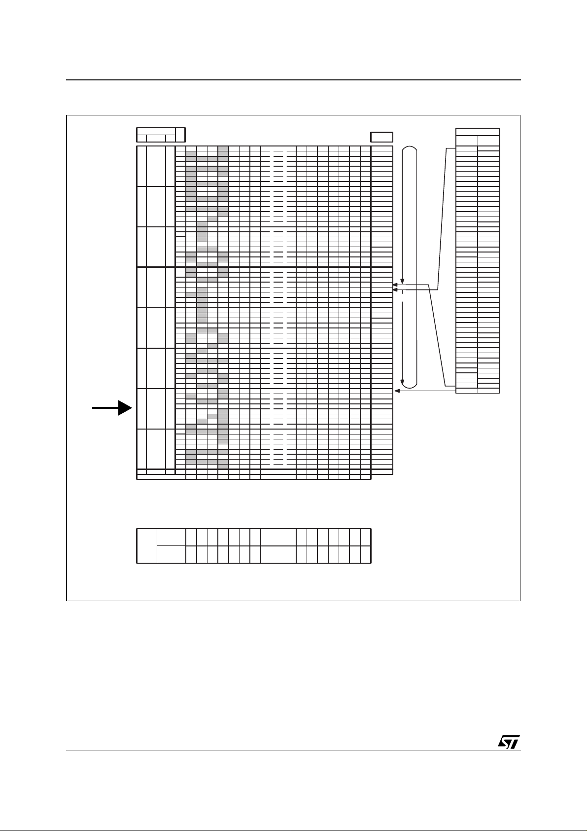
STE2004
Figure 24.
Y-CARRIAGE
Memory Rows vs. Row Drivers Mapping ICON_MODE=1, Y-Carriage=8, Scrolling Pointer<10h and MUX 49
Y Address
D3
D2 D1 D0
0
0
0
0
0
0
0
0
1
X address
D
a
t
a
D0
D1
D2
D3
0
0
0
D4
D5
D6
D7
D0
D1
D2
D3
0
1
0
D4
D5
D6
D7
D0
D1
D2
D3
1
0
0
D4
D5
D6
D7
D0
D1
D2
D3
1
1
0
D4
D5
D6
D7
D0
D1
D2
D3
0
0
1
D4
D5
D6
D7
D0
D1
D2
D3
0
1
1
D4
D5
D6
D7
D0
D1
D2
D3
1
0
1
D4
D5
D6
D7
D0
D1
D2
D3
1
1
1
D4
D5
D6
D7
0
0
0
D0
00H
02H 06H03H 04H 05H
01H
Page 0
Page 1
Page 2
Page 3
Page 4
Page 5
Page 6
Page 7
Page 8
5FH
60H
61H 65H62H 63H 64H
Line
Address
00H
01H
02H
03H
04H
05H
06H
07H
08H
09H
0AH
0BH
0CH
0DH
0EH
0FH
10H
11H
12H
13H
14H
15H
16H
17H
18H
19H
1AH
1BH
1CH
1DH
1EH
1FH
20H
21H
22H
23H
24H
25H
26H
27H
28H
29H
2AH
2BH
2CH
2DH
2EH
2FH
30H
31H
32H
33H
34H
35H
36H
37H
38H
39H
3AH
3BH
3CH
3DH
3EH
3FH
Scrolling Pointer
ROW Output
Normal
direction
R0
R1
R2
R3
R4
R5
R6
R7
R8
R9
R10
R11
R12
R13
R14
R15
R16
R17
R18
R19
R20
R21
R22
R23
R32
R33
R34
R35
R36
R37
R38
R39
R40
R41
R42
R43
R44
R45
R46
R47
R48
R49
R50
R51
R52
R53
R54
R55
R56
Reverse
direction
R55
R54
R53
R52
R51
R50
R49
R48
R47
R46
R45
R44
R43
R42
R41
R40
R39
R38
R37
R36
R35
R34
R33
R32
R23
R22
R21
R20
R19
R18
R17
R16
R15
R14
R13
R12
R11
R10
R9
R8
R7
R6
R5
R4
R3
R2
R1
R0
R56
20/67
COL
Output
Normal
Direction
Reverse
Direction
101
C
C
C
C
O
L
C
O
L
100 99
C
O
O
L
L
C
C
O
O
L
L
98 979695
C
O
L
0
C
O
L
C
C
C
O
O
O
L
L
L
C
C
C
O
O
O
L
L
L
C
C
C
O
L
C
O
L
6
C
O
O
O
L
L
L
C
C
C
O
O
O
L
L
L
4
5
C
O
O
O
L
L
L
1011 2 3 4 5 6 1009998979695
C
C
C
O
O
O
L
L
L
0
123
LR0273
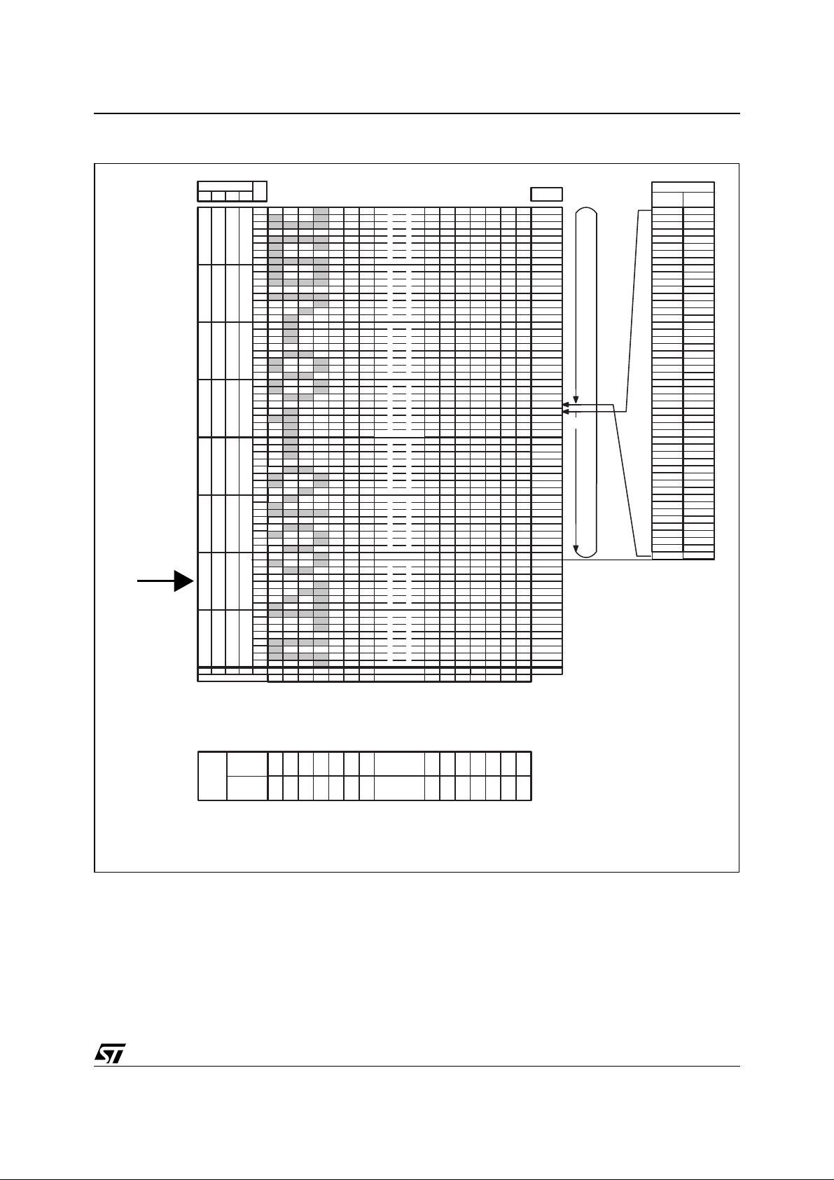
STE2004
Figure 25.
Y-CARRIAGE
Memory Rows vs. Row Drivers Mapping ICON_MODE=0, Y-Carriage=8, Scrolling Pointer<10h and MUX 49
Y Address
D3
D2 D1 D0
0
0
0
0
0
0
0
0
0
1
0
1
0
1
0
1
0
1
X address
D
a
t
a
D0
D1
D2
D3
0
0
D4
D5
D6
D7
D0
D1
D2
D3
0
1
D4
D5
D6
D7
D0
D1
D2
D3
1
0
D4
D5
D6
D7
D0
D1
D2
D3
1
1
D4
D5
D6
D7
D0
D1
D2
D3
0
0
D4
D5
D6
D7
D0
D1
D2
D3
0
1
D4
D5
D6
D7
D0
D1
D2
D3
1
0
D4
D5
D6
D7
D0
D1
D2
D3
1
1
D4
D5
D6
D7
0
0
D0
00H
02H 06H03H 04H 05H
01H
Page 0
Page 1
Page 2
Page 3
Page 4
Page 5
Page 6
Page 7
Page 8
5FH
60H
61H 65H62H 63H 64H
Line
Address
00H
01H
02H
03H
04H
05H
06H
07H
08H
09H
0AH
0BH
0CH
0DH
0EH
0FH
10H
11H
12H
13H
14H
15H
16H
17H
18H
19H
1AH
1BH
1CH
1DH
1EH
1FH
20H
21H
22H
23H
24H
25H
26H
27H
28H
29H
2AH
2BH
2CH
2DH
2EH
2FH
30H
31H
32H
33H
34H
35H
36H
37H
38H
39H
3AH
3BH
3CH
3DH
3EH
3FH
Scrolling Pointer
ROW Output
Normal
direction
R0
R1
R2
R3
R4
R5
R6
R7
R8
R9
R10
R11
R12
R13
R14
R15
R16
R17
R18
R19
R20
R21
R22
R23
R32
R33
R34
R35
R36
R37
R38
R39
R40
R41
R42
R43
R44
R45
R46
R47
R48
R49
R50
R51
R52
R53
R54
R55
R56
Reverse
direction
R56
R55
R54
R53
R52
R51
R50
R49
R48
R47
R46
R45
R44
R43
R42
R41
R40
R39
R38
R37
R36
R35
R34
R33
R32
R23
R22
R21
R20
R19
R18
R17
R16
R15
R14
R13
R12
R11
R10
R9
R8
R7
R6
R5
R4
R3
R2
R1
R0
COL
Output
Normal
Direction
Reverse
Direction
101
C
C
C
C
O
L
C
O
L
100 99
C
O
O
L
L
C
C
O
O
L
L
98 979695
C
O
L
0
C
O
L
C
C
C
O
O
O
L
L
L
C
C
C
O
O
O
L
L
L
C
C
C
O
L
C
O
L
6
C
O
O
O
L
L
L
C
C
C
O
O
O
L
L
L
4
5
C
O
O
O
L
L
L
1011 2 3 4 5 6 1009998979695
C
C
C
O
O
O
L
L
L
0
123
LR0274
21/67
 Loading...