

查询STE2001DIE1供应商
65 X 128 SINGLE CHIP LCD CONTROLLER / DRIVER
STE2001
PRODUCT PREVIEW
■
65 x 128 bits Display Data RAM
■
Configurable matrix: 65 x 128 or 33 x 128
■
Programmable (65/33) MUX rate
■
Row byRow Scrolling
■ Automatic data RAM Blanking procedure
■
Selectable Input Interface:
• I2C Bus Fast and Hs-mode (read and write)
• Parallel Interface (write only)
• Serial Interface (write only)
■
Fully Integrated Oscillator requires no external
components
■
Fully IntegratedConfigurable LCD biasvoltages
generator with:
•Selectable (5X, 4X, 3X, 2X) multiplication factor
• Effective sensing for High Precision Output
• Four selectable temperature compensation
coefficients
■
Designed for chip-on-glass (COG) applications
■ Programmable bottom row pads mirroring and
top row pads mirroring for compatible with both
TCP and COG applications
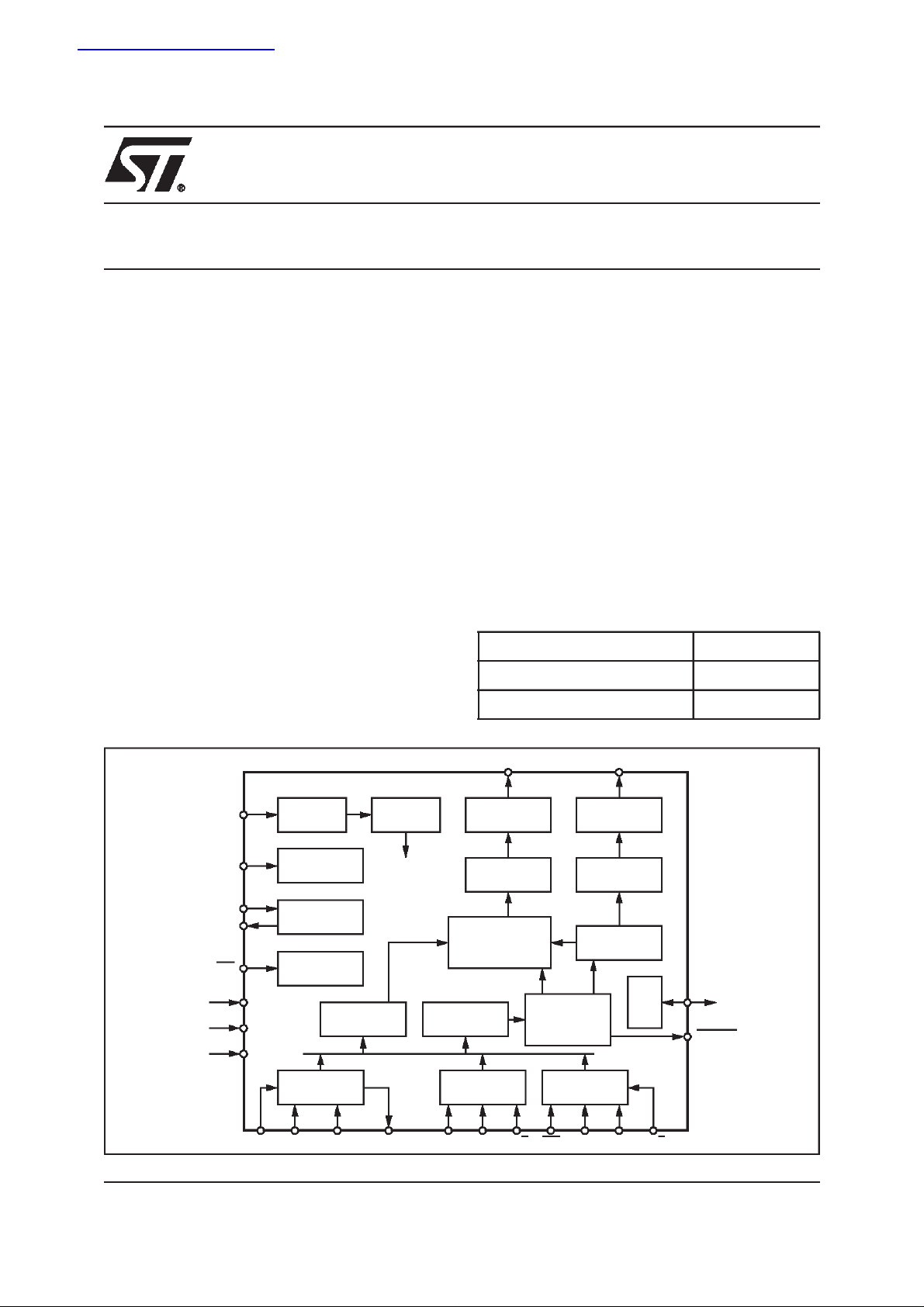
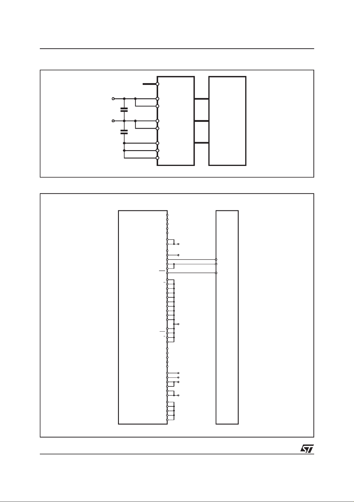
Figure 1. Block Diagram
■
Low Power Consumption, suitable for battery
operated systems
■
Logic Supply Voltage range from 1.9 to 5V
■
High Voltage Generator Supply Voltage range
from 2.4 to 4.5V
■
Display Supply Voltage range from 4.5 to 9V
DESCRIPTION
The STE2001 is a low power CMOS LCD controller
driver. Designed to drive a 65 rows by 128 columns
graphic display, provides all necessary functions in a
single chip, including on-chip LCD supply and bias
voltages generators, resulting in a minimum of externals components and in a very low power consumption. TheSTE2001 features three standard interfaces
(Serial, parallel, I
host
µcontroller.
Bumped Wafers STE2001DIE1
Bumped Dice on WafflePack STE2001DIE2
2
C) for ease of interfacing with the
Type Ordering Number
CO to C127 R0 to R64
OSC
VLCDIN
VLCDSENSE
VLCDOUT
RES
VDD1,2,3
V
1,2
SS
SEL1,2
SAO
DATA
TIMING
GENERATOR
CLOCK
INSTRUCTION
REGISTER
OSC
VOLTAGE
BIAS
GENERATOR
VOLTAGE
HIGH
GENERATOR
RESET
REGISTER
I2CBUS
SDA_IN SDA_OUTSCL DB0 to DB7 E PD/C
COLUMN
DRIVERS
LATCHES
65 x
RAM
PARALLEL
DATA
128
DISPLAY
CONTROL
LOGIC
SCE SDIN SCLK SD/C
SERIAL
ROW
DRIVERS
SHIFT
REGISTER
SCROLL
LOGIC
October 2001
This ispreliminary information on a new product now in development. Details are subject to change without notice.
TEST
TEST_0_13
BSY_FLG
D00IN1137
1/36

STE2001
PIN DESCRIPTION
N° Pad Type Function
R0 to R64 1 to 16
O LCD Row Driver Output
145 to 177
257 to 272
C0 to C127 17 to 144 O LCD Column Driver Output
V
SS1,2
V
DD1
V
DD2,3
V
LCDIN
V
LCDOUT
V
LCDSENSE
227 to 238 GND Ground pads. V
186 to 191 Supply IC Positive Power Supply
192 to 201 Supply Internal Generator Supply Voltages.
246 to 251 Supply LCD Supply Voltages forthe Column and Row Output Drivers.
239 to 244 Supply Voltage Multiplier Ouput
245 Supply Voltage Multiplier Regulation Input. V
is GND for V
SS1
Tuning
SEL1,2 183, 184 I Interface Mode Selection
SDA_IN 223 I
SDA_OUT 222 O
SCL 224 I
SA0 225 I
2
C Bus Data In
I
2
C Bus Data Out
I
2
C bus Clock
I
2
C Slave Address LSB
I
OSC 185 I External Oscillator Input
DD1,VSS2
LCDOUT
for V
DD2
and V
DD3
Sensing for Output Voltage Fine
RES 221 I Reset Input. Active Low.
DB0 to
211 to 218 I Parallel Interface 8 BitData Bus
DB7
E 220 I Parallel Interface Data Latch Signal. Data are Latched on the Falling EDGE.
PD/C 219 I Parallel Interface Data/Command Selector
SDIN 207 I Serial InterfaceData Input
SCLK 210 I Serial InterfaceClock
SCE 209 I Serial Interface ENABLE. When Low the Incoming Dataare Clocked In.
SD/C 208 I Serial InterfaceData/Command selection
BSYFLG 206 O Active Procedure Flag. Notice if There is an ongoing Internal Operation. Active
Low.
T1 to T13 178 to 181
I/O Test Pads.
202 to 205
226
252 to 256
2/36
STE2001
ABSOLUTEMAXIMUM RATINGS
Symbol Parameter Value Unit
V
V
DD2,3
V
P
T
DD1
LCD
I
SS
V
I
I
out
P
T
in
tot
stg
Supply Voltage Range - 0.5 to + 6.5 V
Supply Voltage Range - 0.5 to + 5 V
LCD Supply Voltage Range - 0.5 to + 10 V
Supply Current - 50 to +50 mA
Input Voltage(all input pads) -0.5 to V
i
DD2,3
DC Input Current - 10 to + 10 mA
DC Output Current - 10 to + 10 mA
Total Power Dissipation (Tj=85°C) 300 mW
Power Dissipation per Output 30 mW
o
Operating Junction Temperature -40 to + 85 °C
j
Storage Temperature - 65 to150 °C
+ 0.5 V
ELECTRICAL CHARACTERISTICS
DC OPERATION
(V
DD1
= 1.9to V
DD2,3
+ 0.5V; V
= 2.4 to 4.5 V; V
DD2,3
ss1,2
= 0V; V
= 4.5to 9V; T
LCD
=-40to 85°C; unless otherwise
amb
specified)
Symbol Parameter Test Condition Min. Typ. Max. Unit
Supply Voltages
V
DD1
V
DD2,3
V
LCDIN
V
LCDOUT
I(V
I(V
DD2,3
Supply Voltage 1.9
Supply Voltage LCD Voltage Internally
LCD Supply Voltage LCD Voltage Supplied externally 4.5 9 V
LCD Supply Voltage Internally generated; note 1 4.5 9 V
) Supply Current VDD= 2.8V;V
DD1
) Voltage Generator Supply
Current
T
=-20 to 85°C
amb
generated
= 7.6V; 4x
LCD
charge pump; f
=25°C; note 3.
T
amb
sclk
=0;
with VOP = 0 and PRS= 0
with external V
V
=7.6V; VDD=2.8V;
LCD
=0;T
f
sclk
amb
= 7.6V
LCD
=25°C; no display
load; 4x charge pump; note 3,6
F
=0
osc
V
DD2,3
+0.5
1.8
V
DD2,3
+0.5
2.4 4.5 V
815µA
10 15
70 115 µA
V
V
A
µ
3/36

STE2001
ELECTRICAL CHARACTERISTICS
(continued)
Symbol Parameter Test Condition Min. Typ. Max. Unit
I(V
) TotalSupply Current V
DD1,2,3
= 7.6V; VDD=2.8V;
LCD
4x charge pump; f
sclk
=0;T
amb
80 125 µA
=25°C; no displayload; note 3,6
F
=0
osc
I(V
) External LCD Supply Voltage
LDCIN
Current
VDD=2.8V; V
display load; f
=25°C; note 3. F
T
amb
LCD
sclk
=7.6V;no
=0;
osc
=0
15 25 µA
Logic Inputs
V
V
I
Logic LOW voltage level VIN=Vih(tp<10µs) V
IL
Logic HIGH Voltage Level VIN=Vil(tp<10µs) 0.7
IH
Input Current Vin=V
in
SS1
or V
DD1
SS
V
DD
0.3
V
DD
V
DD2,3
+0.5
-1 1 µA
Columnand Row Driver
R
R
V
V
ROWOutput Resistance 12 20 kohm
row
Column Output resistance 12 20 kohm
col
Column Bias voltage accuracy No load -100 100 mV
col
Row Bias voltage accuracy -100 100 mV
row
LCD Supply Voltage
V
LCD
LCD Supply Voltage accuracy;
Internally generated
VDD= 2.8V;V
LCD
= 7.6V;
fsclk=0; Tamb=25 C;
-300 300 mV
no display load; note 2, 3, 6 & 7
TC Temperature coefficient 00 -550
PPM/°C
01 -1350 PPM/°C
10 -1650 PPM/°C
11 -2650 PPM/°C
Notes: 1. The maximum possible V
2. Internalclock
3. When f
4. Power-down mode. During power-down all static currents are switched-off.
5. If external V
6. Tolerance depends on the temperature; (typically zero at T
ature range limit.
7. ForTC0 to TC3
= 0 there is no interface clock.
sclk
, the display load current is not transmitted to I
LCD
voltage that can be generated is dependent on voltage, temperature and (display) load.
LCD
DD
=27°C), maximum tolerance values are measured at the temper-
amb
V
V
AC OPERATION
(V
DD1
= 1.9to V
DD2,3
+ 0.5V; V
= 2.4 to 4.5 V; V
DD2,3
ss1,2
= 0V; V
= 4.5to 9V; T
LCD
=-40to 85°C; unless otherwise
amb
specified)
Symbol Parameter Test Condition Min. Typ. Max. Unit
INTERNAL OSCILLATOR
F
F
OSC
EXT
Internal Oscillator frequency VDD= 2.8V; 20 38 70 kHz
External Oscillator frequency 20 38 100 kHz
4/36
STE2001
ELECTRICAL CHARACTERISTICS
(continued)
Symbol Parameter Test Condition Min. Typ. Max. Unit
F
FRAME
T
VHRL
T
w(RES)
Frame frequency fosc or fext = 38 kHz; note 1 73 Hz
Vdd1 to RES Low note 2 and 10; C
=1µF0 5ms
VLCD
RES LOW pulse width note 3 600 ns
Reset Pulse Rejection T
=25°C; note 11 370 µs
amb
Reset Pulse Rejection note 11 200
T
START
T
VDD
2
I
C BUS INTERFACE (See note 4)
F
SCL
T
SCLL
T
SCLH
T
SCLL
T
SCLH
T
SU;DAT
T
HD;DAT
T
SU;DAT
T
HD;DAT
T
SU;STA
T
SU;STA
T
HD;STA
T
HD;STA
T
SU;STO
T
SU;STO
T
T
T
rCL1
T
rCL1
T
T
T
T
Reset Pulse vs. Device Ready 1 ms
0
SCL Clock Frequency Fast Mode ;V
=18V; T
V
DD1
High Speed Mode; Cb=100pF
(max); note 6; V
High Speed Mode; Cb=400pF
(max); note 6 ; V
=4.5V DC 400 kHz
DD1
= -20 to 70°C 400 kHz
amb
DC 3.4 MHz
=4.5V
DD1
DC 1.7 MHz
=4.5V
DD1
Cb=100pF 160 ns
Cb=100pF 160 ns
Cb=400pF 320 ns
Cb=400pF 320 ns
Cb=100pF 30 ns
Cb=100pF 30 ns
Cb=400pF 30 ns
Cb=400pF 30 ns
Cb=100pF Note 8 170 ns
Cb=400pF Note 8 330 ns
Cb=100pF Note 8 170 ns
Cb=400pF Note 8 330 ns
Cb=100pF Note 8 170 ns
Cb=400pF Note 8 330 ns
Cb=100pF Note 5, 8 25 ns
rCL
Cb=400pF Note 5, 8 50 ns
rCL
Cb=100pF Note 5, 8 30 ns
Cb=400pF Note 5, 8 120 ns
Cb=100pF Note 5, 8 30 ns
rDA
Cb=400pF Note 5, 8 120 ns
rDA
Cb=100pF Note 5, 8 25 ns
fCL
Cb=400pF Note 5, 8 50 ns
fCL
s
µ
5/36

STE2001
ELECTRICAL CHARACTERISTICS
(continued)
Symbol Parameter Test Condition Min. Typ. Max. Unit
T
T
C
Cb=100pF 25 ns
fDA
Cb=400pF 120 ns
fDA
Capacitive load for SDAH and
b
100 400 pF
SCLH
C
Capacitive load for SDAH + SDA
b
400 pF
line and SCLH + SCL line
T
SW
note 5 10 ns
PARALLEL INTERFACE
T
CY(EN)
T
W(EN)
T
SU(A)
T
H(A)
T
SU(D)
T
H(D)
Enable Cycle Time VDD= 4.5V;Write 125 ns
Enable Pulse width VDD= 4.5V;Write 60 ns
Address Set-up Time VDD= 4.5V;Write 30 ns
Address Hold Time VDD= 4.5V;Write 50 ns
Data Set-Up Time VDD= 4.5V;Write 30 ns
Data Hold Time VDD= 4.5V;Write 50 ns
SERIAL INTERFACE
F
SCLK
T
T
PWH1
T
PWL1
T
T
T
PWH2
T
T
T
T
T
CYC
Clock Frequency VDD= 4.5V 8 MHz
V
= 1.8V 5 MHz
DD1
Clock Cycle SCLK VDD= 4.5V 125 ns
SCLK pulse width HIGH VDD= 4.5V 70 ns
SCLK Pulse width LOW VDD= 4.5V 70 ns
SCE setup time 50 ns
S2
SCE hold time 50 ns
H2
SCE minimum high time 60 ns
SCE start hold time Note 8 60 ns
H5
SD/C setup time 60 ns
S3
SD/C hold time 40 ns
H3
SDIN setup time 40 ns
S4
SDIN hold time 40 ns
H4
f
Notes: 1.
F
frame
2. RES may be LOW or HIGH before V
3. If T
w(RES)
4. All timing values are valid within the operatingsupply voltage and ambient temperature ranges and referenced toV
an inputvoltage swing of V
5. Therise and fall times specified here refer to the driver device and arepart of general Hs-mode specification.
6. Thedevice inputs SDA and SCLare filtered and will reject any spike on the bus-lines of with T
7. Cb is thecapacitive load for each bus line.
8. T
H5
9. Forbus line loads Cb between 100 and 400pF the timing parameters must be linearly interpolated
10.C
VLCD
11.If T
w(RES)
osc
----------=
520
goes HIGH.
to V
DD1
DD
is longer than 500ns (typical) a reset may be generated.
SS
is the time from theprevious SCLK positive edge to the negative edge of SCE
is the filteringcapacitor on VLCDOUT
is shorter than max.value a reset pulse is rejected.
SW
6/36
and VIHwith
IL

STE2001
CIRCUITDESCRIPTION
SuppliesVoltages and Grounds
V
andV
DD2
If the internal voltagegenerator is not used, these should be connectedto V
This supply voltage could be different form V
InternalSupply Voltage Generator
The IC has a fullyintegrated (no external capacitorsrequired)charge pump for the Liquid CrystalDisplay supplyvoltage generation. The multiplyingfactor can be programmed to be: X5; X4; X3; X2, using the ’set CP Multiplication’
Command. The output voltage (V
ferent temperaturecoefficients(TC, rateof changewithtemperature) can beprogrammedusing the bitsTC1 and TC0.
This will ensure no contrast degradation over theLCD operating range. Using the internal charge pump, the V
and V
LCDOUT
without using the internal generator. In such event the V
internal voltagegenerator must be programmed to zero (PRS = 0, Vop = 0 - Reset condition).
Oscillator
A fully integrated oscillator (requires no externalcomponents) is present to provide the clock for the DisplaySystem.
Whenused theOSCpadmustbeconnectedtoVDD1pad. Anexternaloscillatorcouldbeused andfedintotheOSCpin.
DisplayData RAM
The STE2001, provides an 65X128 bits Static RAM to store Display data. This is organized into 8 (Bank0 to
Bank7) banks with 128 Bytes and one Bank (Bank8) with 128 Bits to be used for icons. RAM access is accomplished in either one of the Bus Interfaces provided (seebelow). Allowed addresses are X0 to X127 (Horizontal)
and Y0 to Y8 (Vertical). When writing to RAM, four addressing mode are provided:
• NormalHorizontal (MX = 0 and V = 0), having the column with address X = 0 locatedon the left ofthe memorymap.
The Xpointerisincreased after each byte written. After the lastcolumnaddress(X = 127), Yaddress pointer is modified to jump to nextrow. X restarts fromX = 0 (Fig.2).
• Normal Vertical (MX = 0 and V = 1), having the column with address X = 0 located on the left of the memory map.
The Y pointeris increased after each byte written. After the last row address (Y = 8), the X pointer is modified to
jump to next column and Y restarting from Y = 0. (Fig. 3).
• Mirrored Horizontal (MX = 1 and V = 0), having the column with address X = 0 located on the right of the memory
map. The X pointer is increased after each byte written. After the last column address (X = 127), Y address pointer
is modified to jump to nextrow. X restarts from X = 0 (fig. 4).
• Mirrored Vertical (MX =1 andV = 1), havingthe columnwith address X = 0 located onthe rightof the memory map.
The Y pointeris increased after each byte written. After the last row address (Y = 8), the X pointer is modified to
jump to next column and Y restarting from Y = 0. (Fig. 5).
After the last allowed address (X;Y) = (128;8), the address pointers always jump to the cell with address (X;Y)= (0;0). Data
bytes in the memory couldhave the MSB either on top (D0 = 0, Fig. 6) oron the bottom (D0 = 1, Fig. 7).
are supply voltagesto the internalvoltagegenerator(see below). Theymust be externally connected.
DD3
and V
DD2
) is tightlycontrolled through the V
LCDOUT
DD3.VDD1
must be lower than V
pads must beconnected together. An external supply couldbeconnected to V
LDCOUT
and V
LCDSENSE
pad. V
DD1
LCDSENSE
supplies the rest of the IC.
DD1
+ 0.5V.
DD2,3
pad. For this voltage, four dif-
to supply the LCD
LCDIN
must be connected to GND and the
LCDIN
Mux 65 Mode
The STE2001 provides also means to alter the normal output addressing.A mirroring of the Display along the X axis
is enabled setting to a logic one the MY bit. This function is achievedreading the matrix from physical row 63 to 0,
since the relation between the physical memory rows and the output row drivers is only dependent on the memory
reading sequence (1st row read output on R0, 2nd on R1... last on R65). This function doesn’t affect the content of
the memory map. It is only related to the visualizationprocess (Fig. 8 & Fig. 9).
It is also possible to modify thewhywith whichrow driversare connected withDDRAM memory.A flip along y-axisof
each sub-block can be appliedon both the Row Pads located onthe Interface Side(the edge of the chip where the
Interface Padsare located),setting the TRS bitto a logic one, andon the Row Pads located onthe otheredge,setting
the BRS bitto a logic one.
Figure 2 Automatic data RAM writing sequence with V=0 and Data RAM Normal Format (MX=0) Figure 3 Automatic
data RAM writing sequence with V=1 and Data RAM Normal Format (MX=0)
7/36

STE2001
Figure 2. Automatic data RAM writing sequence with V=0 and Data RAM Normal Format (MX=0)
BANK 0
BANK 1
BANK 2
BANK 3
BANK 4
BANK 5
BANK 6
BANK 7
BANK 8
0123 124125126127
D00IN1138
Figure 3. Automatic data RAM writing sequence with V=1 and Data RAM Normal Format (MX=0)
BANK 0
BANK 1
BANK 2
BANK 3
BANK 4
BANK 5
BANK 6
BANK 7
BANK 8
0 1 2 3 124 125 126 127
D00IN1139
Figure 4. Automatic data RAM writing sequence with V=0 and Data RAM Mirrored Format (MX=1)
BANK 0
BANK 1
BANK 2
BANK 3
BANK 4
BANK 5
BANK 6
BANK 7
BANK 8
127126125124 3210
D00IN1140
Figure 5. Automatic data RAM writing sequence with V=1 and Data RAM Mirrored Format (MX=1)
BANK 0
BANK 1
BANK 2
BANK 3
BANK 4
BANK 5
BANK 6
BANK 7
BANK 8
8/36
127 126 125 124 3 2 1 0
D00IN1141

Figure 6. Data RAM Byte organization with D0 = 0
MSB
0
1 2 3 124 125 126 127
BANK 0
BANK 1
BANK 2
BANK 3
LSB
BANK 4
BANK 5
BANK 6
BANK 7
BANK 8
Figure 7. Data RAM Byte organization with D0 = 1
LSB
0
1 2 3 124 125 126 127
MSB
BANK 0
BANK 1
BANK 2
BANK 3
BANK 4
BANK 5
BANK 6
BANK 7
BANK 8
STE2001
D00IN1142
D00IN1143
Figure 8. Output drivers rows and physical memory rows correspondence with MY =0
PHYSICAL MEMORY ROWROW DRIVER
0
R0
R1
R2
R3
R4
R5
R60
R61
R62
R63
R64
ROW 0
ROW 1
ROW 2
ROW 3
ROW 4
ROW 5
ROW 60
ROW 61
ROW 62
ROW 63
ROW 64
1 2 3 124 125 126 127
D00IN1144
Figure 9. Output drivers rows and physical memory rows correspondence with MY =1
PHYSICAL MEMORY ROWROW DRIVER
0
R63
R62
R61
R60
R59
R58
R3
R2
R1
R0
R64
ROW 0
ROW 1
ROW 2
ROW 3
ROW 4
ROW 5
ROW 60
ROW 61
ROW 62
ROW 63
ROW 64
1 2 3 124 125 126 127
D00IN1145
9/36
STE2001
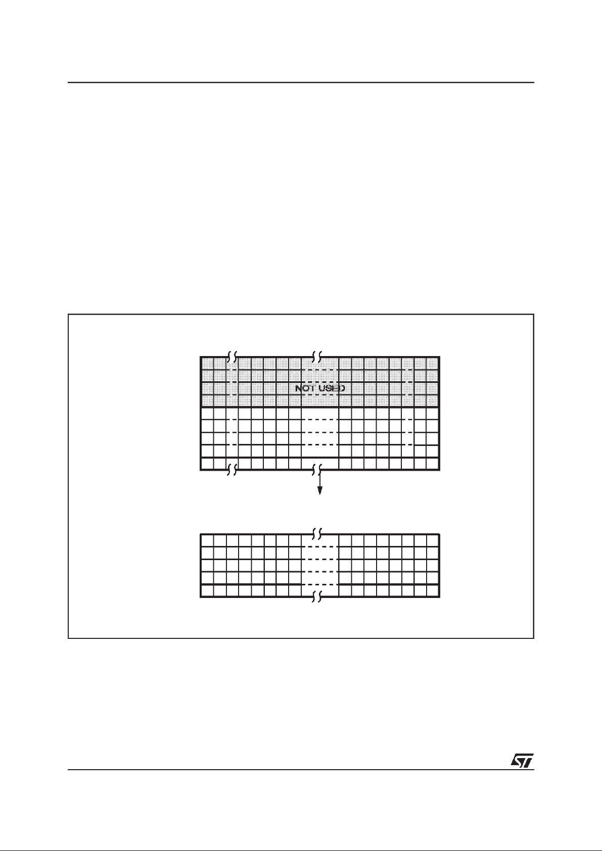
MUX 33 Mode
When using the 1:33 MUX ratio (MUX bit Set), the memory map is changed so that the only”active” row drivers
are the ones related to Bank4 to Bank7.
When writing data RAM, as for Mux 65, four addressing mode are provided. The memory matrix is written as in
mux 65 mode so the user must take care of updating X and Y pointers to fill the memory matrix in the correct
way.
In MUX 33 mode only the MUX 33 memory logic matrix is read. The MY bit control the reading process. If MY
is set to a logic zero the row reading sequence is 0-1-2..........33 (fig.11). If MY is set to a logic one the reading
sequence is 32....1-33 (Fig12).
The icon row (BANK8) is always the last being output either MY bit is a logic one or zero.
The functions relatedto bit TRS is the same as in MUX 65 mode.
In fig. 11 is shown the output drivers pad connection for MUX 33 mode. Note that the unused BANK 0-3 row
drivers become columns drivers.
If a 33x128 LCD matrix is driven, the output row drivers R0-R15and R32-R47 must be floating.
Figure 10. Physical 65x128 memory matrix and 33x128 correspondence
0 1 14 15 16 17 18 112 113110 111109 126127
BANK 0
BANK 1
BANK 2
BANK 3
BANK 4
BANK 5
BANK 6
BANK 7
BANK 8
NOT USED
D00IN1146
10/36
R16-R23
R24-R31
R48-R55
R56-R63
R64
C1
C0C3C2C5C4C7C6
C121
C120
C123
C122
C124
C125
C126
D00IN1147
C127

Figure 11. Output drivers rows and logical memory rows correspondence with MY = 0
ROW DRIVER MUX 33PHYSICAL MEMORY ROW
STE2001
R16
R23
R24
R31
R48
R55
R56
R63
R64 Row 32
Row 0
to
Row 7
Row 8
to
Row15
Row 16
to
Row 23
Row 24
to
Row 31
01234567 123 124 125121 122120 126127
to
to
to
to
BANK 4
BANK 5
BANK 6
BANK 7
BANK 8
D00IN1148
Figure 12. Output drivers rows and logical memory rows correspondence with MY = 1
ROW DRIVER MUX 33PHYSICAL MEMORY ROW
R16
R23
R24
R31
R48
R55
R56
R63
R64 Row 32
Row 0
to
Row 7
Row 8
to
Row15
Row 16
to
Row 23
Row 24
to
Row 31
01234567 123 124 125121 122120 126127
to
to
to
to
BANK 4
BANK 5
BANK 6
BANK 7
BANK 8
D00IN1148
InstructionSet
Two different instructions formats are provided:
- With D/C set to LOW
commands are sent to the Control circuitry.
- With D/C set to HIGH
the Data RAM is addressed Instructions have the syntax summarized in Table.1.
Reset (RES)
At power-on, all internal registers and RAM content are not defined. A Reset pulse mustbe applied on RES pad
(active low) toinitialize the internal registers content (see Tables 3,4,5,&6). Every on-going communication with
the host controller is interrupted. The IC after the reset pulse is programmed in Power Down mode.
The Default configurations is:
- Horizontaladdressing (V = 0)
- Normal instruction set (H = 0)
- Normal display (MX = MY = TRS =BRS = 0)
- MUX 65 mode (MUX= 0)
11/36

STE2001
- Displayblank (E = D = 0)
- Address counter X[6: 0] = 0 and Y[3 : 0] = 0
- Temperature coefficient (TC[1 : 0] = 0)
- Bias system (BS[2 : 0] = 0)
=0
-V
OP
- Power Down(PD = 1)
To clear the RAM content a MEMORY BLANK instruction should be executed.
PowerDown (PD = 1)
When atPowerDown, all LCD outputs are kept at VSS(display off). Biasgenerator and V
(V
LCDOUT
output is discharged to VSS, andthen is possible to disconnect V
LCDOUT
). The internal Oscillator is in
off state. An external clock can be provided. The RAM contents is not cleared.
ChargePump Factor
The desired Charge Pump Multiplication Factor can be programmedthough the S1 and S0 bits, as follows:
S1 S0 Multiplication Factor
002X
013X
104X
115X
generator are OFF
LCD
At Reset the X2 factor is selected.
Bias Levels
To properly drive the LCD, six (Including VLCD and VSS) different voltage (Bias)levels are generated. The ratios among these levels and VLCD, shouldbe selected according to the MUX ratio (m).They are established to
be (Fig. 14):
LCD
------------ -
,
+
n4
V
V
+
n3
LCD
+
n2
-------------
,
+
n4
V
LCD
2
------------ -
,
+
n4
V
LCD
1
------------ -
,
+
n4
V
LCD,VSS
Figure 13. Bias level Generator
V
R
R
nR
R
R
LCD
n+3
n+4
n+2
n+4
2
n+4
1
n+4
V
SS
·V
LCD
·V
LCD
·V
LCD
·V
LCD
D00IN1150
12/36
STE2001
thus providing an 1/(n+4) ratio, with n calculated from:
nm3
For m = 65, n = 5 and an 1/9 ratio is set.
For m = 33, n =3 and an 1/7 ratio is set.
The STE2001 provides three bits (BS0, BS1, BS2) for programming the desired Bias Ratio as shown below:
BS2 BS1 BS0 n
0007
0016
0105
0114
1003
1012
1101
1110
–=
The following table Bias Level for m = 65 and m = 33 are provided:
Symbol m = 65 (1/9) m = 33 (1/7)
V1 V
LCD
V2 8/9*V
V3 7/9*V
V4 2/9*V V
V5 1/9 *V
V6 V
SS
LCD
LCD
LCD
LCD
V
LCD
6/7* V
5/7* V
2/7* V
1/7* V
V
LCD
LCD
LCD
LCD
SS
LCD Voltage Generation
The LCD Voltage at reference temperature (To = 35°C) can be set using the VOP register content according to
the following formula:
V
LCD
(T=To) = V
o = (Ai+VOP· B) (i=0,1)
LCD
with the following values:
Symbol Value Unit Note
Ao 2.90 V PRS = 0
A1 6.91 V PRS = 1
B 0.034 V
To 35 °C
Note that the two PRS value produces two adjacent ranges for VLCD. If the register and PRS bit are set to zero
13/36

STE2001
the internal voltage generator is switched off.
The proper value for the VLCD is a function of the Liquid Crystal Threshold Voltage (Vth) and of the Multiplexing
Rate. A general expression for this is:
+
1m
------------------------ ----------- - V
V
LCD(to)
op
----------------------- ------------------=
V
⋅
21
= 6.85 · V
6.85 VthA
⋅()
0.03
For MUX Rate m = 65 the ideal V
than:
LCD
is:
V
LCD
TemperatureCoefficient
As theviscosity, and therefore the contrast, of theLCD are subjecttochange with temperature, there’s the need
to vary the LCD Voltage with temperature. The STE2001 provides the possibility to change the VLCD in a linear
fashion against temperature with four different Temperature Coefficient selectable through the TC0 and TC1
bits.
TC1 TC0 Value Unit
0 0 -550 PPM/°C
---------–
1
m
th
–
⋅=
th
i
0 1 -1350 PPM/°C
1 0 -1650 PPM/°C
1 1 -2650 PPM/°C
Figure 14. VLCD Slopes Cross Point with Different TC
V
LCD
D01IN1256/mod
35ºC
TEMP
14/36

Figure 15.
V
A
LCD
0
STE2001
B
A
1
A0+B
D01IN1257
V
O
Finally, the V
01h00h 03h 05h02h 04h 7Dh 7Eh 7Fh 00h 01h 02h 03h 04h 05h7Ch 7Dh7Eh 7Fh7Ch
voltage at a given (T) temperature can be calculated as:
LCD
PRS=0
V
LCD
(T) = V
o · [1 + (T-To) · TC]
LCD
PRS=1
MemoryBlanking Procedure
This instruction allows to fill the memory with ”blank” patterns, in order to delete patterns randomly generated
in memory when starting up the device. This instruction substitutes (128X9) single ”write” instructions. It is possible to program ”MemoryBlanking Procedure” only under the following conditions:
- X address = 0
- Y address = 0
-Vbit =0
- PD bit = 0
- MX bit = 0
The end of the procedure will be notified on the BSY_FLG pad going HIGH (while LOW the procedure is running). Any instruction programmed with BSY_FLG LOW will be ignored that is, no instruction can be programmed for a period equivalent to 128X9 internal write cycles (128X9X1/fclock). The start of Memory blanking
procedure will be between one and two fclock cycles from the last active edge (E rising edge for the parallel
interface, last SCLK rising edge for the Serial interface, last SCLrising edge for the I
2
C interface).
CheckerBoard Procedure
This instruction allows to fill the memory with ”checker-board” pattern. It is mainly intended to developers, who
can now simply obtain complexmodule test configuration by means of a single instruction. It is possible to program ”Checker Board Procedure” only under the following conditions:
- X address = 0
- Y address = 0
-Vbit =0
- PD bit = 0
- MX bit = 0
15/36

STE2001
The end ofthe procedure will be notified ontheBSY_FLG pad going HIGH, while LOW the procedure is running.
Any instruction programmed withBSY_FLG LOW will be ignored, that is, no instructioncan be programmed for
a period equivalent to 128X9 internal write cycles (128X9X1/fclock). The start of Memory blanking procedure
will be between one and two fclock cycles fromthe last active edge (Erisingedge for the parallel interface, last
SCLK rising edge for the Serial interface, last SCL risingedge for the I
Scroll
The STE2001 can scrollthe graphics display in units of raster-rows. The scrolling function is achieved changing
the correspondence between the rows of the logical memory map and the output row drivers.The scroll function
doesn’t affect the data ram content. It is only related to the visualization process. The information output on the
drivers is related to the row reading sequence (the 1st row read is output on R0, the 2nd on R1 and so on).
Scrolling means reading the matrix starting from a row that is sequentially increased or decreased. After every
scrolling command the offset between the memory address and the memory scanning pointer is increased or
decreased by one. The offset range is between 0 to 63 in mux 65 mode and 0-31 in mux 33 mode. After the
64th scrolling command in mux 65 mode and after the 32th in mux 33 mode, the offset between the memory
address and the memory scanning pointer is again zero (Cyclic Scrolling). Bank8 is always accessed last in
each frame, and so isn’t scrolled.
If the DIR Bitis set to a logic zero the offset register is increased by one and the raster is scrolled from top down. If
the DIR Bit is setto a logic one the offset register is decreased by one and the raster is scrolled from bottom-up.
Bus Interfaces
To provide the widest flexibility and ease of use the STE2001 features three different methods for interfacing
the host Controller. To select the desired interface the SEL1 and SEL2 pads need to be connected to a logic
LOW (connect to GND) or a logic HIGH (connect to VDD). All the I/O pins of the unused interfaces must be
connected to GND. If I/O pins voltage is lower than VDD interfaces could sink more current than expected.
All interfaces are working while the STE2001 is in Power Down.
SEL2 SEL1 Interface Note
00
0 1 Serial Write only
1 1 Parallel Write only
1 0 Not Used
2
C interface).
2
C
I
Read and Write; Fastand
High Speed Mode
I2C Interface
The I2C interface is a fully complying I2C bus specification, selectable to work in both Fast (400kHz Clock) and
High Speed Mode (3.4MHz).
This bus isintended for communication between different Ics. It consists of twolines: one bi-directional for data
signals (SDA) and one for clock signals (SCL). Both the SDA and SCL lines must be connected to a positive
supply voltage via an active or passive pull-up.
The following protocol has been defined:
- Data transfer may be initiated only when the bus is not busy.
- During data transfer, thedata line mustremainstable whenever the clock line is high. Changes in the data line
while the clock line is high will be interpreted as control signals.
Accordingly, the following bus conditions have been defined:
BUS not busy: Both data and clock lines remain High.
StartData Transfer: Achange in the state of the data line, from High to Low, while the clock is High,define the
START condition.
16/36

STE2001
Stop Data Transfer:
A Change in the state of the data line, from low to High, while the clock signal is High,
defines the STOP condition.
Data Valid: The state of the data line represents valid data when after a start condition, the data line is stable
for the duration of the High periodof theclock signal. The data on the linemay be changed during the Low period
of the clock signal. There is one clock pulse per bit of data.
Each data transfer is initiated with a start condition and terminated with a stop condition. The number of data
bytes transferred between the start and the stop conditions is not limited. The information is transmitted bytewide and each receiver acknowledges with the ninth bit.
By definition, adevice that gives outa message is called ”transmitter”, the receivingdevice that gets the signals
is called ”receiver”. The device that controls the message is called ”master”. The devices that are controlled by
the master are called ”slaves”
Acknowledge. Each byte of eight bits is followed by one acknowledge bit. This acknowledge bit is a low level
put on the bus by the receiver, whereas the master generates an extra acknowledge related clock pulse.
A slave receiver which is addressed must generate an acknowledge after the reception of each byte. Also, a
master receiver must generate an acknowledge after the reception of each byte that has been clocked out of
the slave transmitter. The device that acknowledges has to pull down the SDA_IN line during the acknowledge
clock pulse. Of course, setup and hold time must be taken into account. A master receiver must signal an endof-data to the slavetransmitter by not generating an acknowledge on the last byte that has been clocked out of
the slave. In this case, the transmitter must leave the data line High to enable themaster to generate the STOP
condition.
Connecting SDA_IN and SDA_OUT together the SDA line become the standard data line. Having the acknowledge output (SDAOUT) separated from the serial data line is advantageous in Chip-On-Glass
(COG) applications. In COG applications where thetrack resistance from the SDAOUT pad to thesystem
SDA line can be significant, a potential divider is generated by the bus pull-up resistor and the Indium Tin
Oxide (ITO) track resistance. It is possible that during the acknowledge cycle theSTE2001 will not be able
to create a valid logic 0 level. Bysplitting the SDAinput fromthe outputthe device could be usedin a mode
that ignores the acknowledge bit. In COG applications where the acknowledge cycle is required, it is necessary to minimize the track resistance from the SDACK pad to the system SDA line to guarantee a valid
LOW level.
To be compliant with the I2C-bus Hs-mode specification the STE2001 is able to detect the special sequence
”S00001xxx”. After this sequence no acknowledge pulse is generated.
Since no internal modification are applied to work in Hs-mode, the device is able to work in Hs-mode without
detecting the master code.
Figure 16. Bit transfer and START,STOP conditions definition
DATA
LINE
STABLE
DATA VALID
CLOCK
DATA
START
CONDITION
CHANGE
DATA ALLOWED
OF
D00IN1151
STOP
CONDITION
17/36

STE2001
Figure 17. Acknowledgment on theI
START
SCLK
FROM
MASTER
DATA OUTPUT
BY TRANSMITTER
DATA OUTPUT
BY RECEIVER
Figure 18. I
2
C-bustimings
SDAH
SCLH
RES
t
SU;STA
t
fDA
t
START
Sr
2
C-bus
1
MSB LSB
t
rDA
t
HD;DAT
t
HD;STA
t
t
rCL
t
HIGH
289
D00IN1152
t
SU;DAT
fCL
t
LOW
= MCScurrent source pull-up = Rp resistor pull-up
t
rCL1
(1) (1)
t
t
LOW
HIGH
CLOCK PULSE
ACKNOWLEDGEMENT
t
rCL1
D00IN1153
FOR
Sr P
CommunicationProtocol
The STE2001 is an I2C slave. The accesstothe device is bi-directional sincedata write and status read are allowed.
Two are the device addresses available for the device. Both have in commonthe first 6 bits (011110). The leastsignificantbit of the slave address is set by connectingthe SA0 inputto a logic 0 or to a logic 1.
To start the communication betweenthe bus masterand the slave LCD driver, the master must initiate a START condition.Followingthis,the mastersends an 8-bit byte, shown in Fig. 18, on the SDAbus line (Most significant bitfirst).
This consists of the 7-bit Device selectCode, andthe 1-bitRead/Write Designator (R/W).
All slaves with the corresponding address acknowledge in parallel,all the others willignore the I2C-bus transfer.
WritingMode.
If the R/W bit is set to logic 0 the STE2001 is set to be a receiver. After the slaves acknowledge one or more
command word follows to define the status of the device.
A command word is composed by two bytes. The first is a control byte which defines the Co and D/C values,
the second is a data byte (fig 18). The Co bitis the command MSB and defines if after this command willfollow
one data byte and an other command word or if will follow a stream of data (Co = 1 Command word, Co = 0
Stream of data). The D/C bit defines whether the data byte is a command or RAM data (D/C = 1 RAM Data, D/
C = 0 Command).
If Co =1 and D/C = 0 the incoming data byte isdecoded as a command, and if Co =1 and D/C =1, the following
data byte will be stored in the data RAM at the location specified by the data pointer.
E very byte of a command word must be acknowledged by all addressed units.
After the last control byte, if D/Cis set to alogic 1the incoming data bytes are stored inside theSTE2001 Display
RAM starting at the address specified by the data pointer. The data pointer is automatically updated after every
byte writtenand in the end points to the last RAM location written.
Every byte must be acknowledged by all addressed units.
ReadingMode.
If the R/W bit is set to logic 1 the chip will output data immediately after the slave address. If the D/C bit sent
during the last write access, is set to a logic 0, the byte read is the status byte.
18/36

Figure 19. communication protocol
WRITE MODE
STE2001 ACK
STE2001 ACK
STE2001
STE2001 ACK STE2001 ACK STE2001 ACK
SS0111100A0A
R/W
SLAVE ADDRESS
READ MODE
STE2001 ACK MASTER
SS0111100A1A
R/W
Co
COMMAND WORD CONTROL BYTE MSB........LSB
D01IN1247
A1 DC Control Byte DATA Byte ADC ControlByteA 0 DATA Byte A P
Co LAST N> 0 BYTE
P
0111100AR/
STE2001
SLAVE ADDRESS
S
W
C oD
000000A
C
CONTROL BYTE
SERIALINTERFACE
The STE2001 serial Interface is a unidirectional link between the display driver and the application supervisor.
It consists of four lines: one for data signals (SDIN), one forclock signals (SCLK), one for the peripheral enable
(SCE) and one for mode selection (SD/C).
The serial interface is active only if the SCE line is set to a logic 0. When SCE line is high the serial peripheral
power consumption is zero.
The STE2001is alwaysa slave on the bus and receive the communication clockon the SCLK pin from the mas-
ter. The STE2001 is only able to receive data.
Information are exchanged byte-wide. Duringdata transfer, the data line issampled on the positive SCLK edge.
While SCE pin is high the serial interface is kept in reset.
SD/C line status indicates whether the byte is a command (SD/C =0) or RAM data (SD/C =1);it is read on the
eighth SCLK clock pulse during every byte transfer.
If SCEstays low after the last bit of a command/data byte, the serial interface expects the MSB of thenext byte
at the next SCLK positive edge.
A reset pulse onRES pin interrupts the transmission. No data is written into the data RAM and all the internal
registers are cleared.
If SCE is low after the positive edge ofRES, the serial interface is readyto receive data.
19/36

STE2001
Figure 20. Serial bus protocol - one byte transmission
SCE
D/C
SCLK
SDIN
MSB LSB
Figure 21. Serial bus protocol - several byte transmission
SCE
D/C
SCLK
SDIN
DB7 DB6 DB5 DB4 DB3 DB2 DB1 DB0 DB7 DB6 DB5 DB4 DB3 DB2 DB1 DB0 DB7 DB6 DB5
Figure 22. RESET effect on the serial interface
t
S2
D00IN1159
D00IN1160
t
H2
t
PWH2
20/36
SCE
D/C
SCLK
SDIN
RES t
START
t
S3
t
PWL1
t
H5
t
H3
t
WH1
t
S4
t
H4
t
CYC
t(
H5)
t
S2
D00IN1161

STE2001
ParallelInterface
The STE2001 parallel Interface isa unidirectional linkbetween the display driver and the application supervisor.
It consists of ten lines: eight data lines (from DB7 to DB0) and two control lines. The control lines are: enable
(E) for data latch and PD/C for mode selection.
The data lines and the control line values are internally latched on E rising edge (fig. 23).
Figure 23. Parallel interface timing
PD/C
t
SU(D)
t
HO(D)
t
W(en)
t
h(A)
t
CY(en)
D00IN1162
E
DB0-DB7
RES t
START
t
SU(A)
Table 1. Instruction Set
Instruction D/C R/W Description
B7 B6 B5 B4 B3 B2 B1 B0
H=0 or H=1
NOP 0000000000 NoOperation
Function Set 0 0 0 0 1 MX MY PD V H PowerDown Management; Entry
Mode; Extended Instruction Set
Read Status Byte 0 1 PD
TRS BRS D E MX MY DO
Write Data 1 0 D7 D6 D5 D4 D3 D2 D1 D0 Writes data to RAM
H=0
Memory Blank 0 0 0 0000001Starts Memory Blank Procedure
Scroll 0 0 0 000001DIRScrolls by one RowUP or DOWN
Range Setting 000000010PRS V
V
LCD
Display Control 0 0 0 0001D0E Select Display Configuration
Set CP Factor 0 0 0 00100S1S0Charge Pump Multiplication Factor
Set RAM Y 0 0 0 1 0 0 Y3 Y2 Y1 Y0 Set Horizontal (Y) RAM Address
Set RAM X 0 0 1 X6 X5 X4 X3 X2 X1 X0 Set Vertical (X) RAM Address
H=1
Checker Board 0 0 0 0000001Starts Checker Board Procedure
Multiplex Select 0 0 0 000001
TC Select 0 0 0 00001TC1TC0
MUX Selects MUX factor
SetTemperatureCoefficientforV
Output Address 0 0 0 0001DOTRS BRS Set Row Order on Output Pads
BiasRatios 0000010BS2BS1BS0 Setdesired Bias Ratios
Reserved 0 0 0 1 X X X X X X Not to be used
Set V
OP
001OP6 OP5 OP4 OP3 OP2 OP1 OP0 VOPregister Write instruction
2
(I
C interface only )
programmingrangeselection
LDC
LDC
21/36

STE2001
Table 2. Explanations of Table 6 symbols
BIT 0 1
DIR Scroll by one down Scroll by one up
H Use basic instruction set Use extended instruction set 0
PD Device fully working Devicein power down 1
V Horizontal addressing Vertical addressing 0
MX Normal X axis addressing X axis address is mirrored. 0
MY Image is displayed not vertically mirrored Image is displayed vertically mirrored 0
TRS No top rows mirroring Toprows mirroring (row pads 16-31 & 48-64) 0
BRS No bottom rows mirroring Bottom rows mirroring (row pads 0-15 & 32-47) 0
DO MSB on TOP MSB on BOTTOM 0
RESET
STATE
PRS V
MUX 1:65 multiplexing ratio 1:33 multiplexing ratio 0
= 2.94V V
LCD
= 6.75V 0
LCD
Table 3.
D E DESCRIPTION RESET STATE
0 0 displayblank
1 0 normal mode D=0
0 1 all display segments on E=0
1 1 inverse video mode
Table 4.
S1 S0 DESCRIPTION RESET STATE
0 0 Multiplication Factor 2X
0 1 Multiplication Factor 3X 0
1 0 Multiplication Factor 4X
1 1 Multiplication Factor 5X
Table 5.
TC1 TC0 DESCRIPTION RESET STATE
0 0 VLCD temperature Coefficient 0
0 1 VLCD temperature Coefficient 1 00
1 0 VLCD temperature Coefficient 2
1 1 VLCD temperature Coefficient 3
22/36

Table 6.
BS2 BS1 BS0 DESCRIPTION RESET STATE
0 0 0 Bias Ratio equal to 7
0 0 1 Bias Ratio equal to 6
0 1 0 Bias Ratio equal to 5
0 1 1 Bias Ratio equal to 4 000
1 0 0 Bias Ratio equal to 3
1 0 1 Bias Ratio equal to 2
1 1 0 Bias Ratio equal to 1
1 1 1 Bias Ratio equal to 0
Figure 24. Application Schematic Using an External LCD Voltage Generator
I/O
VDD2,3
V
DD
100nF
V
SS
VDD1
VSS2
VSS1
32
128
65 x 128
DISPLAY
STE2001
1µF
V
LCD
VLCDSENSE
VLCDOUT
VLCDIN
33
D00IN1157
Figure 25. Application Schematicusing the Internal LCD VoltageGenerator and two separatesupplies
I/O
V
DD2
V
100nF 100nF
V
SS
1µF
DD1
VLCDSENSE
VLCDOUT
VDD2,3
VDD1
VSS2
VSS1
VLCDIN
32
128
33
65 x 128
DISPLAY
D00IN1158
23/36
STE2001
Figure 26. Application Schematic using the Internal LCD Voltage Generator and a single supply
I/O
V
DD
VDD2,3
VDD1
100nF
V
SS
VSS2
VSS1
1µF
VLCDSENSE
VLCDOUT
VLCDIN
Figure 27. Pad Configuration with I2C interface
TEST_13
TEST_12
TEST_11
TEST_10
TEST_8
VSS2
VSS1
TEST 9
SA0
SCL
SDAIN
SDAOUT
STE2001 µP
RES
PD/C
SCLK
SCE
SD/C
SDIN
BSY_FLG
TEST_7
TEST_6
TEST_5
TEST_4
VDD3
VDD2
VDD1
OSCIN
SEL1
SEL2
VSSOUT
TEST_3
TEST_2
TEST_1
TEST_0
E
D0
D1
D2
D3
D4
D5
D6
D7
32
128
33
GND
VDD1/GND/VSSOUT
VDD1
GND/VSSOUT
D01IN1261
65 x 128
DISPLAY
D00IN1156
24/36

Figure 28. Pad Configuration with Parallel interface
TEST_13
TEST_12
TEST_11
TEST_10
TEST_8
VSS2
VSS1
SA0
SCL
RES
PD/C
SCLK
SCE
SD/C
SDIN
VDD3
VDD2
VDD1
OSC
SEL1
SEL2
E
D0
D1
D2
D3
D4
D5
D6
D7
GND
VDD1/GND/VSSOUT
VDD1
VDD1
GND/VSSOUT
VDD1
TEST 9
SDAIN
SDAOUT
STE2001 µP
BSY_FLG
TEST_7
TEST_6
TEST_5
TEST_4
VSSOUT
TEST_3
TEST_2
TEST_1
TEST_0
STE2001
D01IN1262
Figure 29. Pad Configuration with Serial interface
TEST_13
TEST_12
TEST_11
TEST_10
TEST_8
VSS2
VSS1
TEST 9
SA0
SCL
SDAIN
SDAOUT
STE2001 µP
RES
PD/C
SCLK
SCE
SD/C
SDIN
BSY_FLG
TEST_7
TEST_6
TEST_5
TEST_4
VDD3
VDD2
VDD1
OSCIN
SEL1
SEL2
VSSOUT
TEST_3
TEST_2
TEST_1
TEST_0
E
D0
D1
D2
D3
D4
D5
D6
D7
GND
VDD1/GND/VSSOUT
VDD1
VDD1
VDD1
GND/VSSOUT
D01IN1263
25/36

STE2001
Figure 30. Power OFF Timing Diagram
VDD2/3
VDD1
RES
INPUTS
Figure 31. Power OFF Sequence
POWER OFF SEQUENCE
t
VDD
D01IN1264
SET by Software (PD=0) or (Vop=0& PRS=[0;0])
Force Active Input Lines Low
REMOVE VDD1
REMOVEVDD2/3
END OF POWEROFF SEQUENCE
D01IN1265
26/36

Figure 32. Power-Up & RESET timing diagram
STE2001
VDD2/3
VDD1
RES
INPUTS
t
VDD
Figure 33. Power-Up & RESET timing diagram
VDD2/3
t
VDD1
RES
INPUTS
VDD
t
W(RES)
t
VHRL
t
W(RES)
D01IN1189
D01IN1190
Figure 34. Power Up Sequence
POWER UP SEQUENCE
Set Active Input lines low
Apply a RESET Pulse
Apply VDD2/3
Apply VDD1
END OF POWER UP
(STE2001 in Reset State)
SEQUENCE
D01IN1266
27/36

STE2001
Figure 35. Chip Mechanical Drawing
ROW 0
ALIGNEMENT MARK
STE2001
ROW16
ROW 15
COL 0
COL 63
COL 64
ALIGNEMENT MARK
(0,0)
Y
X
ROW31
TEST
VLCDIN
VLCDSENSE
VLCDOUT
VSS2
VSS1
TEST
SA0
SCL
SDAIN
SDAOUT
RES
E
PD/C
D0
D1
D2
D3
D4
D5
D6
D7
SCLK
SCE
SD/C
SDIN
BSY_FLG
TEST
28/36
COL 127
ROW 47
ROW 32
ALIGNEMENT MARK
ALIGNEMENT MARK
D01IN1191
VDD2
VDD3
VDD1
OSC
SEL1
SEL2
VSSOUT
TEST
ROW64
ROW48

Figure 36. Improved ALTH & PLESKO Driving Method
V
LCD
V
2
V
3
ROW 0
R0 (t)
V
4
V
5
V
SS
V
LCD
V
2
V
3
ROW 1
R1 (t)
V
4
V
5
V
SS
V
LCD
V
2
V
3
COL 0
C0 (t)
V
4
V
5
V
SS
V
LCD
V
2
V
3
COL 1
C1 (t)
V
4
V
5
V
SS
V
LCD-VSS
V
3-VSS
STE2001
∆V1(t)
(t)
∆V
2
V
V
state1
state2
V
LCD-V2
(t)
V
3-VSS
V
LCD-VSS
V
3-VSS
V
LCD-V2
(t)
V3-V
∆V
(t) = C1(t) - R0(t)
1
(t) = C1(t) - R1(t)
∆V
2
0V
0V
SS
0123456789 64
.......
FRAME n FRAME n + 1
0123456789 64.....
.....
.......
V
4-V5
0V
VSS-V
V4-V
VSS-V
V
4-V5
0V
VSS-V
V4-V
VSS-V
D00IN1154
5
LCD
LCD
5
LCD
LCD
29/36

STE2001
Figure 37. DATA RAM to display Mapping
DISPLAYDATA RAM
bank
0
bank
1
bank
2
bank
3
bank
7
bank
8
GLASS
TOPVIEW
DISPLAYDATA RAM = ”1”
DISPLAYDATA RAM = ”0”
LCD
ICOR ROW
Table 7. Test Pin Configuration
Test Numb. Pin
TEST_0
TEST_1
TEST_2
TEST_3
TEST_4
TEST_5
TEST_6
TEST_7
T8
T9
TEST_10
TEST_11
TEST_12
TEST_13
30/36
D00IN1155
GND
GND
GND
GND
OPEN
OPEN
OPEN
OPEN
OPEN
OPEN
OPEN
OPEN
OPEN
OPEN

STE2001
Table 8. Mechanical Dimensions
Die Size 2.12mmX12.5mm
Pad Pitch
Pad Size
Bump Dimensions
WFS Thickness
70 µm
62µmX100µm
50µmX88µmX17.5
500µm
Table 9. Pad Coordinates
NAME PAD X (µm) Y(µm)
R0 1 -5,994 -898.2
R1 2 -5,924 -898.2
R2 3 -5,854 -898.2
R3
R4 5 -5,714 -898.2
R5
R6 7 -5,574 -898.2
R7 8 -5,504 -898.2
R8 9 -5,434 -898.2
R9 10 -5,364 -898.2
R10
R11 12 -5,224 -898.2
R12
R13 14 -5,084 -898.2
R14 15 -5,014 -898.2
R15 16 -4,944 -898.2
C0 17 -4,591.8 -898.2
C1
C2 19 -4,451.8 -898.2
C3
C4 21 -4,311.8 -898.2
C5 22 -4,241.8 -898.2
C6 23 -4,171.8 -898.2
C7 24 -4,101.8 -898.2
C8
C9 26 -3,961.8 -898.2
C10
C11 28 -3,821.8 -898.2
C12 29 -3,751.8 -898.2
4 -5,784 -898.2
6 -5,644 -898.2
11 -5,294 -898.2
13 -5,154 -898.2
18 -4,521.8 -898.2
20 -4,381.8 -898.2
25 -4,031.8 -898.2
27 -3,891.8 -898.2
Table 9. Pad Coordinates
NAME PAD X (µm) Y(µm)
C13 30 -3,681.8 -898.2
C14 31 -3,611.8 -898.2
C15 32 -3,541.8 -898.2
C16 33 -3,471.8 -898.2
C17
C18 35 -3,331.8 -898.2
C19
C20 37 -3,191.8 -898.2
C21 38 -3,121.8 -898.2
C22 39 -3,051.8 -898.2
C23 40 -2,981.8 -898.2
C24
C25 42 -2,841.8 -898.2
C26
C27 44 -2,701.8 -898.2
C28 45 -2,631.8 -898.2
C29 46 -2,561.8 -898.2
C30 47 -2,491.8 -898.2
C31
C32 49 -2,351.8 -898.2
C33
C34 51 -2,211.8 -898.2
C35 52 -2,141.8 -898.2
C36 53 -2,071.8 -898.2
C37 54 -2,001.8 -898.2
C38
C39 56 -1,861.8 -898.2
C40
C41 58 -1,721.8 -898.2
C42 59 -1,651.8 -898.2
C43 60 -1,581.8 -898.2
C44 61 -1,511.8 -898.2
C45
C46 63 -1,371.8 -898.2
C47
C48 65 -1,231.8 -898.2
C49 66 -1,161.8 -898.2
34 -3,401.8 -898.2
36 -3,261.8 -898.2
41 -2,911.8 -898.2
43 -2,771.8 -898.2
48 -2,421.8 -898.2
50 -2,281.8 -898.2
55 -1,931.8 -898.2
57 -1,791.8 -898.2
62 -1,441.8 -898.2
64 -1,301.8 -898.2
(continued)
31/36

STE2001
Table 9. Pad Coordinates
NAME PAD X (µm) Y(µm)
C50 67 -1,091.8 -898.2
C51 68 -1,021.8 -898.2
C52 69 -951.8 -898.2
C53 70 -881.8 -898.2
C54
C55 72 -741.8 -898.2
C56
C57 74 -601.8 -898.2
C58 75 -531.8 -898.2
C59 76 -461.8 -898.2
C60 77 -391.8 -898.2
C61
C62 79 -251.8 -898.2
C63
C64 81 175.44 -898.2
C65 82 245.44 -898.2
C66 83 315.44 -898.2
C67 84 385.44 -898.2
C68
C69 86 525.44 -898.2
C70
C71 88 665.44 -898.2
C72 89 735.44 -898.2
C73 90 805.44 -898.2
C74 91 875.44 -898.2
C75
C76 93 1,015.44 -898.2
C77
C78 95 1,155.44 -898.2
C79 96 1,225.44 -898.2
C80 97 1,295.44 -898.2
C81 98 1,365.44 -898.2
C82
C83 100 1,505.44 -898.2
C84
C85 102 1,645.44 -898.2
C86 103 1,715.44 -898.2
71 -811.8 -898.2
73 -671.8 -898.2
78 -321.8 -898.2
80 -181.8 -898.2
85 455.44 -898.2
87 595.44 -898.2
92 945.44 -898.2
94 1,085.44 -898.2
99 1,435.44 -898.2
101 1,575.44 -898.2
(continued)
Table 9. Pad Coordinates
NAME PAD X (µm) Y(µm)
C87 104 1,785.44 -898.2
C88 105 1,855.44 -898.2
C89 106 1,925.44 -898.2
C90 107 1,995.44 -898.2
C91
C92 109 2,135.44 -898.2
C93
C94 111 2,275.44 -898.2
C95 112 2,345.44 -898.2
C96 113 2,415.44 -898.2
C97 114 2,485.44 -898.2
C98
C99 116 2,625.44 -898.2
C100
C101 118 2,765.44 -898.2
C102 119 2,835.44 -898.2
C103 120 2,905.44 -898.2
C104 121 2,975.44 -898.2
C105
C106 123 3,115.44 -898.2
C107
C108 125 3,255.44 -898.2
C109 126 3,325.44 -898.2
C110 127 3,395.44 -898.2
C111 128 3,465.44 -898.2
C112
C113 130 3,605.44 -898.2
C114
C115 132 3,745.44 -898.2
C116 133 3,815.44 -898.2
C117 134 3,885.44 -898.2
C118 135 3,955.44 -898.2
C119
C120 137 4,095.44 -898.2
C121
C122 139 4,235.44 -898.2
C123 140 4,305.44 -898.2
108 2,065.44 -898.2
110 2,205.44 -898.2
115 2,555.44 -898.2
117 2,695.44 -898.2
122 3,045.44 -898.2
124 3,185.44 -898.2
129 3,535.44 -898.2
131 3,675.44 -898.2
136 4,025.44 -898.2
138 4,165.44 -898.2
(continued)
32/36

STE2001
Table 9. Pad Coordinates
NAME PAD X (µm) Y(µm)
C124 141 4,375.44 -898.2
C125 142 4,445.44 -898.2
C126 143 4,515.44 -898.2
C127 144 4,585.44 -898.2
R47
R46 146 5,013.84 -898.2
R45
R44 148 5,153.84 -898.2
R43 149 5,223.84 -898.2
R42 150 5,293.84 -898.2
R41 151 5,363.84 -898.2
R40
R39 153 5,503.84 -898.2
R38
R37 155 5,643.84 -898.2
R36 156 5,713.84 -898.2
R35 157 5,783.84 -898.2
R34 158 5,853.84 -898.2
R33
R32 160 5,993.84 -898.2
R48
R49 162 5,951.92 898.2
R50 163 5,881.92 898.2
R51 164 5,811.92 898.2
R52 165 5,741.92 898.2
R53
R54 167 5,601.92 898.2
R55
R56 169 5,461.92 898.2
R57 170 5,391.92 898.2
R58 171 5,321.92 898.2
R59 172 5,251.92 898.2
R60
R61 174 5,111.92 898.2
R62
R63 176 4,971.92 898.2
R64 177 4,901.92 898.2
145 4,943.84 -898.2
147 5,083.84 -898.2
152 5,433.84 -898.2
154 5,573.84 -898.2
159 5,923.84 -898.2
161 6,021.92 898.2
166 5,671.92 898.2
168 5,531.92 898.2
173 5,181.92 898.2
175 5,041.92 898.2
(continued)
Table 9. Pad Coordinates
NAME PAD X (µm) Y(µm)
TEST_3 178 4,640.52 898.2
TEST_2 179 4,500.68 898.2
TEST_1 180 4,360.84 898.2
TEST_0 181 4,221 898.2
VSSOUT
SEL2 183 4,011.16 898.2
SEL1
OSC 185 3,731.48 898.2
VDD1_1 186 3,661.48 898.2
VDD1_2 187 3,591.48 898.2
VDD1_3 188 3,521.48 898.2
VDD1_4
VDD1_5 190 3,381.48 898.2
VDD1_6
VDD3_1 192 3,223.08 898.2
VDD3_2 193 3,153.08 898.2
VDD3_3 194 3,083.08 898.2
VDD2_1 195 2,994.68 898.2
VDD2_2
VDD2_3 197 2,854.68 898.2
VDD2_4
VDD2_5 199 2,714.68 898.2
VDD2_6 200 2,644.68 898.2
VDD2_7 201 2,574.68 898.2
TEST_7 202 2,033.84 898.2
TEST_6
TEST_5 204 1,754.16 898.2
TEST_4
BSY_FLAG 206 1,474.48 898.2
SDIN 207 1,333.2 898.2
SD/C 208 1,193.36 898.2
SCE 209 1,053.52 898.2
SCLK
D7 211 773.84 898.2
D6
D5 213 494.16 898.2
D4 214 354.32 898.2
182 4,151 898.2
184 3,871.32 898.2
189 3,451.48 898.2
191 3,311.48 898.2
196 2,924.68 898.2
198 2,784.68 898.2
203 1,894 898.2
205 1,614.32 898.2
210 913.68 898.2
212 634 898.2
(continued)
33/36

STE2001
Table 9. Pad Coordinates
(continued)
NAME PAD X (µm) Y(µm)
D3 215 214.48 898.2
D2 216 74.64 898.2
D1 217 -65.2 898.2
D0 218 -205.04 898.2
PD/C
219 -344.88 898.2
E 220 -484.72 898.2
RES
SDA_OUT 222 -764.4 898.2
221 -624.56 898.2
SDA_IN 223 -904.24 898.2
SCL 224 -1,044.08 898.2
SA0 225 -1,183.92 898.2
TEST9
226 -1,722.04 898.2
VSS1_1 227 -1,795.48 898.2
VSS1_2
228 -1,865.48 898.2
VSS1_3 229 -1,935.48 898.2
VSS1_4 230 -2,075.88 898.2
VSS1_5 231 -2,145.88 898.2
VSS1_6 232 -2,215.88 898.2
VSS2_1
233 -2,356.28 898.2
VSS2_2 234 -2,426.28 898.2
VSS2_3
235 -2,496.28 898.2
VSS2_4 236 -2,636.68 898.2
VSS2_5 237 -2,706.68 898.2
VSS2_6 238 -2,776.68 898.2
VLCDOUT1 239 -3,545.64 898.2
VLCDOUT2
VLCDOUT3 241 -3,685.64 898.2
VLCDOUT4
VLCDOUT5 243 -3,825.64 898.2
VLCDOUT6 244 -3,895.64 898.2
VLCSENSE 245 -3,968.08 898.2
VLCDIN_1 246 -4,040.48 898.2
VLCDIN_2
VLCDIN_3 248 -4,180.48 898.2
VLCDIN_4
VLCDIN_5 250 -4,320.48 898.2
VLCDIN_6 251 -4,390.48 898.2
240 -3,615.64 898.2
242 -3,755.64 898.2
247 -4,110.48 898.2
249 -4,250.48 898.2
Table 9. Pad Coordinates
(continued)
NAME PAD X (µm) Y(µm)
TEST_12 252 -4,460.48 898.2
TEST_13 253 -4,540.48 898.2
TEST_10 254 -4,620.48 898.2
TEST_11 255 -4,700.48 898.2
TEST_8
256 -4,780.48 898.2
R31 257 -4,971.92 898.2
R30
258 -5,041.92 898.2
R29 259 -5,111.92 898.2
R28 260 -5,181.92 898.2
R27 261 -5,251.92 898.2
R26 262 -5,321.92 898.2
R25
263 -5,391.92 898.2
R24 264 -5,461.92 898.2
R23
265 -5,531.92 898.2
R22 266 -5,601.92 898.2
R21 267 -5,671.92 898.2
R20 268 -5,741.92 898.2
R19 269 -5,811.92 898.2
R18
270 -5,881.92 898.2
R17 271 -5,951.92 898.2
R16
272 -6,021.92 898.2
Table 10. Alignment marks coordinates
X Y MARKS
4806.2 901.8 mark1
-4876.2 901.8 mark2
-6092.6 -901.8 mark3
6092.6 -901.8 mark4
Figure 38. Alignment marks dimensions
34/36

Figure 39.
Figure 40. Tray Information
DIE IDENTIFICATION
R16
STE2001
D01IN1249
PAD
WIDE
CENTERLINE
STE2001
SHRINK
50.6±0.25
45.90
X
DETAIL
MASSTAB5:1
SCHNITT B-B
2 x 14.59 = 29.18±0.25
10.75
2.54 x 45?
PACK
STATPRO150
NOTES: ENGRAVING TOBE 20 CHAIR x 0.3
x 0.05 RAISED CENTER ON
KNOCKDUTS NOT TO EXCEED 0.08
MATERIAL:
BUILD TOOL TO 0.009 MM/MM
TRAYOR WAFFLE
OF STE2000/STE2001
SCHNITT A-A
10º
1
+0.08
0.3
12.80
-0.10
2.46
-0.13
+0.08
3.94
2.18
D01IN1248
Y
DETAIL
MASSTAB5:1
1
2.39
10º
DETAILX
B
4.60
0.90
AA
B
-0.25
+0.13
45.59
STATPROT.150
FLUOROWARE GmbH
13 x 3.19 = 41.47±0.25
DETAILY
35/36

STE2001
Information furnished is believed tobe accurate and reliable. However,STMicroelectronics assumes no responsibility for the consequences
of useof such information nor for any infringementof patents or other rightsof third partieswhich may result from its use. No license is granted
by implication or otherwise under any patent or patent rights of STMicroelectronics. Specifications mentioned in this publication are subject
to change without notice. This publication supersedes and replaces all information previously supplied. STMicroelectronics products arenot
authorized for use as critical components in life support devices or systems without express written approval of STMicroelectronics.
The ST logo is a registered trademark of STMicroelectronics
2001 STMicroelectronics - All Rights Reserved
Australia - Brazil - China - Finland - France - Germany - Hong Kong - India - Italy - Japan - Malaysia - Malta- Morocco - Singapore - Spain
STMicroelectronics GROUP OF COMPANIES
- Sweden- Switzerland - United Kingdom - U.S.A.
http://www.st.com
36/36
 Loading...