

查询STE180NE10供应商
N-CHANNEL 100V - 4.5 mΩ - 180A ISOTOP
TYPE V
DSS
ST E180NE10 100 V < 6 mΩ 180 A
■ TYPICALR
■ 100%AVALANCHETESTED
■ LOW INTRINSICCAPACITANCE
■ GATECHARGE MINIMIZED
■ REDUCEDVOLTAGESPREAD
DS(on)
= 4.5 mΩ
DESCRIPTION
This Power MOSFET is the latest developmentof
STMicroelectronics unique ”Single Feature
Size” strip-based process. The resulting transistor shows extremely high packingdensity forlow
on-resistance, rugged avalance characteristics
and less critical alignment steps therefore a remarkablemanufacturingreproducibility.
APPLICATIONS
■ SMPS& UPS
■ MOTORCONTROL
■ WELDINGEQUIPMENT
■ OUTPUTSTAGE FOR PWM, ULTRASONIC
CIRCUITS
R
DS(on)
I
D
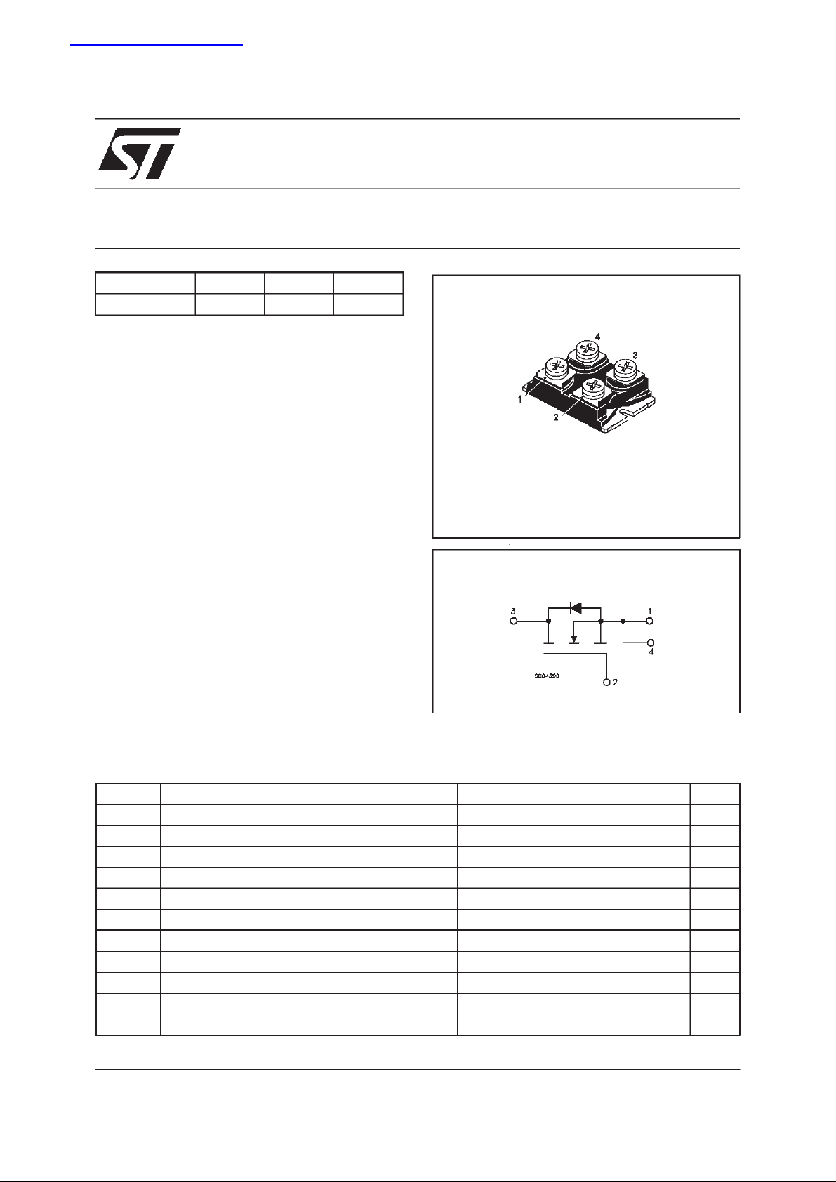
STE180NE10
STripFET POWER MOSFET
ISOTOP
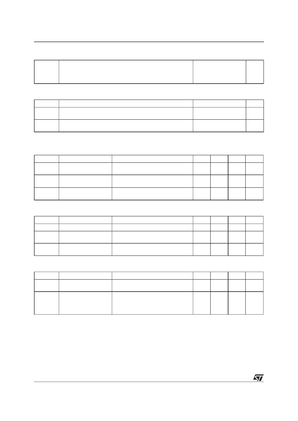
INTERNAL SCHEMATIC DIAGRAM
ABSOLUTE MAXIMUM RATINGS
Symb o l Parameter Value Unit
V
V
V
I
DM
P
V
T
(•) Pulse width limited by safe operating area (1)ISD≤
November 1999
Drain-source Volt age (VGS= 0) 100 V
DS
Drain- gate Voltag e (RGS=20kΩ) 100 V
DGR
Gate-s ource Voltage
GS
I
Drain Current (co nt inuous) at Tc=25oC 180 A
D
I
Drain Current (co nt inuous) at Tc=100oC 119 A
D
20 V
±
(•) Drain Current (pu lsed) 540 A
Tot al Di ss i pat ion at Tc=25oC 360 W
tot
Derat ing Fact or 2.88 W/
Ins ulat i on Withst an d Volt age ( AC-RMS ) 2500 V
ISO
Sto rage Temper at ur e -55 t o 150
stg
T
Max. O per a t ing Junction Temperature 150
j
180
Α,
di/dτ ≤ 200 A/µs, VDD≤ V
(BR)DSS,Tj≤TJMAX
o
C
o
C
o
C
1/8
STE180NE10
THERMAL DATA
R
thj-case
R
thc-h
AVALANCHE CHARACTERISTICS
Symbol Parameter Max V alue Unit
I
AR
E
Ther mal Resistanc e Junct ion-case Max
Ther mal Resistanc e Case-heatsink With conduct iv e
Gr ease A pplied Max
Avalanche Current, Repetitive or Not-Repetitive
(pulse width limited by T
Single P ul s e Avalan c he Energy
AS
(starting T
=25oC, ID=IAR,VDD=25V)
j
max)
j
0.347
0.05
60 A
720 mJ
o
C/W
o
C/W
ELECTRICAL CHARACTERISTICS
=25oC unless otherwisespecified)
(T
case
OFF
Symbol Parameter Test Condit ions Min. Typ. M ax. Unit
V
(BR)DSS
Drain-source
ID=1mA VGS= 0 100 V
Break dow n Voltage
I
DSS
I
GSS
Zero Gate Voltage
Drain Cur rent (V
GS
Gat e- bod y L eak ag e
Current (V
DS
=0)
=0)
V
=MaxRating
DS
=MaxRating Tc= 125oC
V
DS
V
=± 20 V
GS
4
40
400 nA
±
ON(∗)
Symbol Parameter Test Condit ions Min. Typ. M ax. Unit
V
GS(th)
R
DS(on)
Gate Threshold Voltage VDS=VGSID=1mA 234V
Sta t ic Drain -s ource On
VGS=10V ID=90A 4.5 6 m
Resistance
I
D(on)
On State Drain Current VDS>I
D(on)xRDS(on)max
180 A
VGS=10V
DYNAMIC
Symbol Parameter Test Condit ions Min. Typ. M ax. Unit
g
(∗)Forward
fs
Tr ansc on duc tance
C
C
C
Input Capac i t anc e
iss
Out put Capacitanc e
oss
Reverse Tr ansfer
rss
Capacit a nc e
VDS>I
D(on)xRDS(on)maxID
=80A 30 S
VDS=25V f=1MHz VGS=0 21
2.5
0.9
µ
µA
nF
nF
nF
A
Ω
2/8

STE180NE10
ELECTRICAL CHARACTERISTICS
(continued)
SWITCHINGON
Symbol Parameter Test Condit ions Min. Typ. M ax. Unit
t
d(on)
Tur n-on Delay Time
Rise Ti m e
t
r
VDD=50V ID=90A
R
=4.7
G
Ω
VGS=10V
35
100
(Resis t iv e Loa d, see fig. 3 )
Q
Q
Q
Tot al Gat e Charge
g
Gat e- Source Charg e
gs
Gate-Drain Charge
gd
VDD=80V ID=180A VGS= 10 V 142
37
60
185 nC
SWITCHINGOFF
Symbol Parameter Test Condit ions Min. Typ. M ax. Unit
t
d(on)
Tur n-of f D ela y Time
t
Fall T ime
r
VDD=50V ID=90A
=4.7 Ω VGS=10V
R
G
110
100
(Resis t iv e Loa d, see fig. 3 )
t
r(Voff)
t
t
Off-voltage Rise Time
Fall T ime
f
Cross-over T ime
c
VDD=80V ID=180A
=4.7 Ω VGS=10V
R
G
(Indu ct iv e Load, see fig. 5)
100
50
92
SOURCEDRAINDIODE
Symbol Parameter Test Condit ions Min. Typ. M ax. Unit
I
SDM
V
I
SD
Q
I
RRM
SD
t
Source-drain Current
(•)
Source-drain Current
180
540
(pulsed)
(∗)ForwardOnVoltage ISD= 180 A VGS=0 1.5 V
Reverse Recover y
rr
Time
Reverse Recover y
rr
ISD= 180 A di/dt = 100 A /µs
=50V Tj= 150oC
V
DD
(see test circuit, fig. 5)
170
850
Charge
Reverse Recover y
10
Current
ns
ns
nC
nC
ns
ns
ns
ns
ns
A
A
ns
µC
A
(∗) Pulsed: Pulse duration = 300 µs, duty cycle 1.5 %
(•) Pulse width limited by safe operating area
SafeOperating Area ThermalImpedance
3/8

STE180NE10
OutputCharacteristics
Transconductance
TransferCharacteristics
Static Drain-sourceOn Resistance
Gate Charge vs Gate-sourceVoltage
4/8
CapacitanceVariations

STE180NE10
NormalizedGate ThresholdVoltage vs
Temperature
Source-drainDiode Forward Characteristics
NormalizedOn Resistancevs Temperature
5/8

STE180NE10
Fig. 1:
UnclampedInductiveLoad TestCircuit
Fig. 3: Switching Times Test CircuitsFor
ResistiveLoad
Fig. 2:
UnclampedInductive Waveform
Fig. 4: GateChargetest Circuit
Fig. 5:
Test CircuitFor InductiveLoad Switching
And Diode Recovery Times
6/8

ISOTOPMECHANICALDATA
STE180NE10
DIM.
MIN. TYP. MAX. MIN. TYP. MAX.
A 11.8 12.2 0.466 0.480
B 8.9 9.1 0.350 0.358
C 1.95 2.05 0.076 0.080
D 0.75 0.85 0.029 0.033
E 12.6 12.8 0.496 0.503
F 25.15 25.5 0.990 1.003
G 31.5 31.7 1.240 1.248
H 4 0.157
J 4.1 4.3 0.161 0.169
K 14.9 15.1 0.586 0.594
L 30.1 30.3 1.185 1.193
M 37.8 38.2 1.488 1.503
N 4 0.157
O 7.8 8.2 0.307 0.322
mm inch
G
A
B
O
N
D
E
F
H
J
C
K
L
M
7/8

STE180NE10
Information furnishedis believedto be accurate and reliable.However, STMicroelectronics assumes no responsibilityfor the consequences
of use of such information nor for any infringement of patents or other rights of third parties which may result from its use. No licenseis
granted by implication or otherwise under anypatent or patent rights of STMicroelectronics. Specificationmentioned in this publicationare
subjectto change without notice. This publication supersedes and replaces all information previouslysupplied. STMicroelectronics products
are not authorized for use as critical components in lifesupport devices or systems without express written approval of STMicroelectronics.
The ST logo is a trademark of STMicroelectronics
1999 STMicroelectronics – Printed in Italy – All Rights Reserved
STMicroelectronics GROUP OF COMPANIES
Australia - Brazil - China - Finland - France - Germany - Hong Kong - India - Italy - Japan - Malaysia - Malta - Morocco -
8/8
Singapore - Spain - Sweden - Switzerland - United Kingdom - U.S.A.
http://www.st.com
.
 Loading...