

ST STE110NS20FD User Manual
查询STE110NS20FD供应商
STE110NS20FD
N-CHANNEL 200V - 0.022Ω - 110A ISOTOP
MESH OVERLAY™ Power MOSFET
TYPE V
DSS
R
DS(on)
I
D
STE110NS20FD 200V < 0.024Ω 110 A
n
TYPICAL RDS(on) = 0.022Ω
n
EXTREMELY HIGH dv /d t C APABILITY
n
100% AVALANCHE TESTED
n
GATE CHARGE MINIMIZED
n
± 20V GATE TO SOURCE VOLTAGE RATING
n
LOW INTRINSIC CAPACITANCE
n
FAST BODY-DRAIN DIODE:LOW trr, Q
rr
DESCRIPTION
Using the latest high voltage MESH OVERLAY™
process, STMicroelectronics has designed an advanced family of power MOSFETs with outstanding
performances. The new patented S Trip layout coupled with the Company’s proprietary edge termination structure, gives the lowest RDS(ON) per area,
exceptional avalanche and dv/dt capabilities and
unrivalled gate charge and switching characteristics.
APPLICATIONS
n
HIGH CURRENT, HIGH SPEED SWITCHING
n
SWITCH MODE POWER SUPPLY (SM PS)
n
DC-AC CONVERTER FOR WELDING
EQUIPMENT AND UNINTERRUPTABLE
POWER SUPPLY AND MOTOR DRIVE
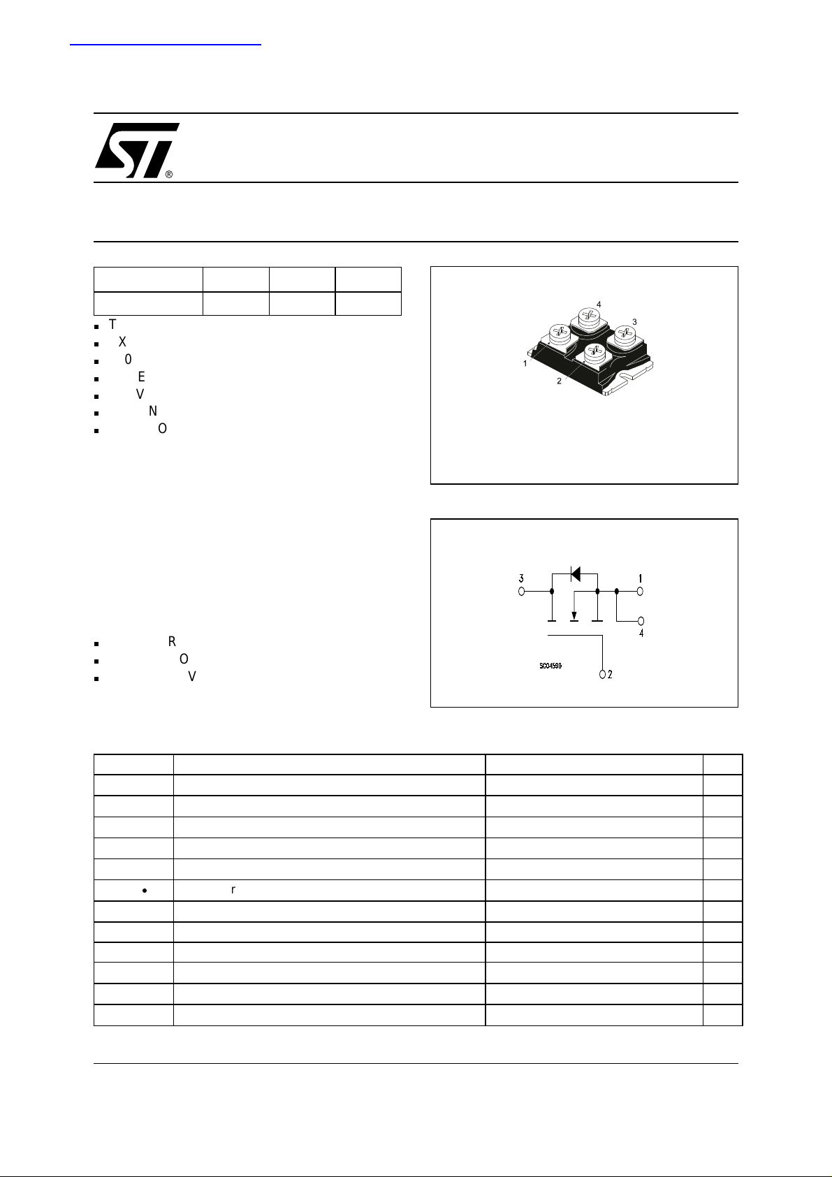
ISOTOP
INTERNAL SCHEMATIC DIAGRAM
ABSOLUTE MAXIMUM RATINGS
Symbol Parameter Value Unit
V
DS
V
DGR
V
GS
I
D
I
D
I
DM
P
TOT
dv/dt (1) Peak Diode Recovery voltage slope 25 V/ns
V
ISO
T
stg
T
j
(•)Pu l se width limited by safe operati ng area
Drain-source Voltage (VGS = 0)
Drain-gate Voltage (RGS = 20 kΩ)
200 V
200 V
Gate- source Voltage ±20 V
Drain Current (continuos) at TC = 25°C
Drain Current (continuos) at TC = 100°C
(l)
Drain Current (pulsed) 440 A
Total Dissipation at TC = 25°C
110 A
69 A
500 W
Derating Factor 4 W/°C
Insulation Winthstand Voltage (AC-RMS) 2500 V
Storage Temperature –65 to 150 °C
Max. Operating Junction Temperature 150 °C
(1)ISD ≤110A, di/dt ≤200A/µs, VDD ≤ V
(BR)DSS
, Tj ≤ T
JMAX
1/8January 2002
STE110NS20FD
THERMA L D ATA
Rthj-case Thermal Resistance Junction-case Max 0.25 °C/W
Rthj-amb Thermal Resistance Junction-ambient Max 30 °C/W
T
l
AVALANCHE CHARACTERISTICS
Symbol Parameter Max Value Unit
I
AR
E
AS
ELECTRICAL CHARACTERISTICS (TCASE = 25 °C UNLESS OTHERWISE SPECIFIED)
OFF
Symbol Parameter Test Conditions Min. Typ. Max. Unit
V
(BR)DSS
I
DSS
I
GSS
Maximum Lead Temperature For Soldering Purpose 300 °C
Avalanche Current, Repetitive or Not-Repetitive
(pulse width limited by T
max)
j
Single Pulse Avalanche Energy
(starting T
Drain-source
= 25 °C, ID = IAR, VDD = 50 V)
j
ID = 250 µA, VGS = 0 200 V
110 A
750 mJ
Breakdown Voltage
Zero Gate Voltage
Drain Current (V
GS
Gate-body Leakage
Current (V
DS
= 0)
= 0)
V
= Max Rating
DS
VDS = Max Rating, TC = 125 °C
V
= ± 20V ±100 nA
GS
10 µA
100 µA
ON
(1)
Symbol Parameter Test Conditions Min. Typ. Max. Unit
V
GS(th)
R
DS(on)
Gate Threshold Voltage
Static Drain-source On
V
= VGS, ID = 250µA
DS
VGS = 10V, ID = 50A
345V
0.022 0.024 Ω
Resistance
DYNAMIC
Symbol Parameter Test Conditions Min. Typ. Max. Unit
(1) Forward Transconductance VDS > I
g
fs
C
iss
C
oss
C
rss
Input Capacitance
Output Capacitance 1500 pF
Reverse Transfer
I
D
V
Capacitance
Note: 1. Pulsed: Pu l se duration = 300 µs, duty cycle 1. 5 %.
= 50A
DS
D(on)
x R
DS(on)max,
= 25V, f = 1 MHz, VGS = 0
30 S
7900 pF
460 pF
2/8
STE110NS20FD
ELECTRICAL CHARACTERISTICS (CONTINUED)
SWITCHING ON
Symbol Parameter Test Conditions Min. Typ. Max. Unit
V
t
d(on)
Q
Q
Q
t
r
gs
gd
Turn-on Delay Time
Rise Time 130 ns
Total Gate Charge
g
Gate-Source Charge 35 nC
Gate-Drain Charge 135 nC
SWITCHING OFF
Symbol Param eter Test Conditions Min. Typ. Max. Unit
t
r(Voff)
t
t
f
c
Off-voltage Rise Time
Fall Time 140 ns
Cross-over Time 220 ns
SOURCE DRAIN DIODE
Symbol Parameter Test Conditions Min. Typ. Max. Unit
I
SD
I
SDM
VSD (1)
t
rr
Q
rr
I
RRM
Note: 1. Pulsed: Pulse duration = 300 µs, duty cycle 1.5 %.
2. Pulse width limi ted by safe operating area.
(2)
Source-drain Current 110 A
Source-drain Current (pulsed) 440 A
Forward On Voltage
Reverse Recovery Time
Reverse Recovery Charg e 1.35 µ C
Reverse Recovery Curren t 12 A
= 100V, ID = 50A
DD
RG= 4.7Ω VGS = 10V
(see test circuit, Figure 3)
V
= 100V, ID = 100A,
DD
V
= 10V
GS
V
= 100V, ID = 100A,
DD
RG= 4.7Ω, V
GS
= 10V
(see test circuit, Figure 5)
ISD = 100A, VGS = 0
I
= 100A, di/dt = 100A/µs,
SD
V
= 160V, Tj = 150°C
DD
(see test circuit, Figure 5)
40 ns
360 504 nC
245 ns
1.6 V
225 ns
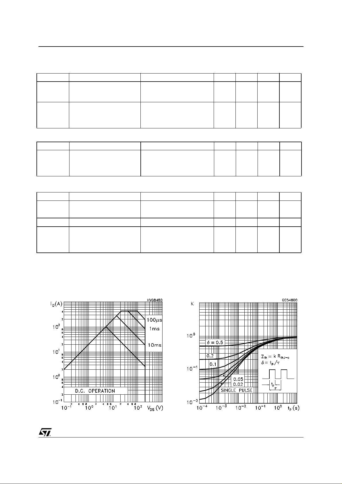
Safe Operating Area
Ther m al Impe d ance
3/8
 Loading...