

查询STE110NA20供应商
N - CHANNEL ENHANCEMENT MODE
TYPE V
DSS
STE11 0NA 20 200 V < 0.019 Ω 110 A
R
DS(on)
STE110NA20
FAST POWER MOS TRANSISTOR
PRELIMINARY DATA
I
D
■ TYPICALR
■ HIGH CURRENTPOWER MODULE
■ AVALANCHERUGGEDTECHNOLOGY
■ VERYLARGE SOA - LARGE PEAK POWER
DS(on)
=0.015 Ω
CAPABILITY
■ EASY TO MOUNT
■ SAMECURRENT CAPABILITYFOR THE
TWOSOURCE TERMINALS
■ EXTREMELYLOW Rth (Junction to case)
■ VERYLOW INTERNALPARASITIC
INDUCTANCE
■ ISOLATEDPACKAGE UL RECOGNIZED
APPLICATIONS
■ SMPS& UPS
■ MOTORCONTROL
■ WELDINGEQUIPMENT
■ OUTPUTSTAGE FOR PWM, ULTRASONIC
CIRCUITS
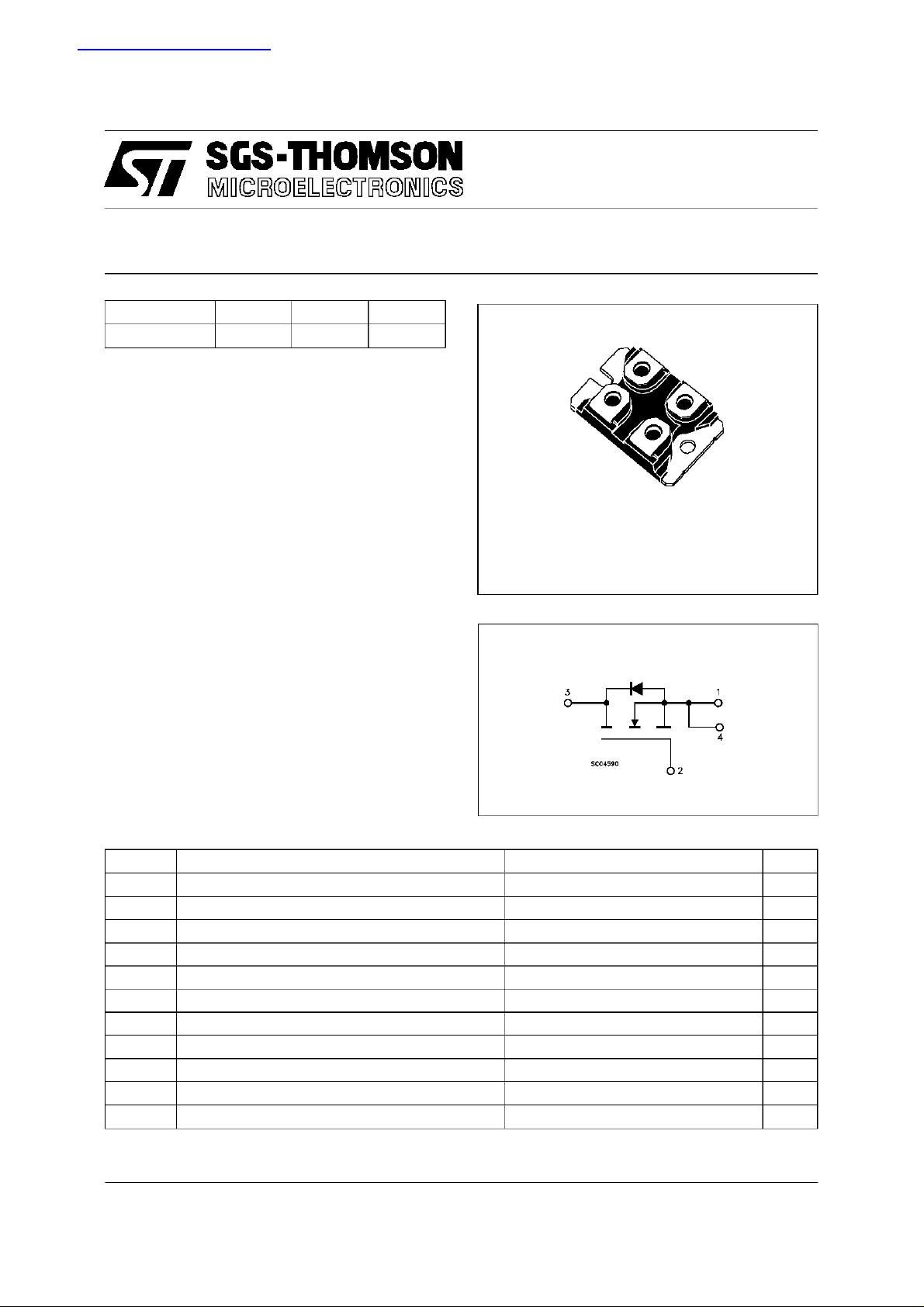
ISOTOP
INTERNAL SCHEMATIC DIAGRAM
ABSOLUTE MAXIMUM RATINGS
Symbol Parameter Value Unit
V
V
V
I
DM
P
T
V
(•) Pulse width limited bysafe operatingarea
March 1996
Drain-source Voltage ( VGS= 0 ) 200 V
DS
Drain- gate Volt age (RGS=20kΩ) 200 V
DGR
Gat e- source Voltage ± 30 V
GS
I
Drain Curren t (co nt inu ous ) at Tc=25oC 110 A
D
I
Drain Curren t (co nt inu ous ) at Tc=100oC73A
D
(•) Drain Current (pulsed) 440 A
Tot al Dissipation at Tc=25oC 450 W
tot
Derating Factor 3.6 W/
St orage Temperatur e -55 to 150
stg
T
Max. Operating Junction Temperatur e 150
j
Ins ulation Withhstand V o lt age (A C- R M S) 2500 V
ISO
o
C
o
C
o
C
1/8
STE110NA20
THERMAL DATA
R
thj-case
R
thc-h
AVALANCHE CHARACTERISTICS
Symb o l Para met er M ax Value Uni t
I
AR
E
E
I
AR
Ther mal Resistance Junct ion-case Max
Ther mal Resistance Case-heatsink Wit h Conduct ive
Gr ease Appli ed Max
Avalanche Current , Repet it iv e or Not-Repe t it ive
(pulse width limi t ed by T
Single Pu lse Avalanc he E nerg y
AS
(starti ng T
Repetitive Avalanche Energy
AR
=25oC, ID=IAR,VDD=50V)
j
(pulse width limi t ed by T
max, δ <1%)
j
max, δ <1%)
j
Avalanche Current , Repet it iv e or Not-Repe t it ive
=100oC, p ulse wid t h limited by Tjmax, δ <1%)
(T
c
0.27
0.05
55 A
500 mJ
175 mJ
32.5 A
o
C/W
o
C/W
ELECTRICAL CHARACTERISTICS (T
=25oC unlessotherwise specified)
case
OFF
Symbol Parameter Test Condition s Min. Typ. Max. Unit
V
(BR)DSS
Drain-source
ID=1mA VGS= 0 200 V
Break dow n Voltage
I
I
DSS
GSS
Zero Gate Voltage
Drain Current (V
GS
Gat e- bod y Leaka ge
Current (V
DS
=0)
=0)
V
=MaxRating
DS
=MaxRatingx0.8 Tc= 125oC
V
DS
V
= ± 30 V ± 400 nA
GS
400
200
ON (∗)
Symbol Parameter Test Condition s Min. Typ. Max. Unit
V
GS(th )
R
DS(on)
I
D(on)
Gat e Thre shold Volt age VDS=VGSID=1mA 2.25 3 3.75 V
St at ic Drain-source On
Resistance
VGS= 10V ID=55A
= 10V ID=55A Tc=100oC
V
GS
On State Drain Current VDS>I
D(on)xRDS(on)max
110 A
0.015 0.019 Ω
VGS=10V
DYNAMIC
Symbol Parameter Test Condition s Min. Typ. Max. Unit
g
(∗)Forward
fs
Tr ansc on ductance
C
C
C
Input Capac it an ce
iss
Out put Capac itance
oss
Reverse Transfer
rss
Capacit a nc e
VDS=15 V ID=55A 38 S
VDS=25V f=1MHz VGS= 0 12.9
2870
980
µA
mA
Ω
nF
pF
pF
2/8
STE110NA20
ELECTRICAL CHARACTERISTICS (continued)
SWITCHINGON
Symbol Parameter Test Condition s Min. Typ. Max. Unit
t
d(on)
t
r
Turn-on Time
Rise Time
VDD=100V ID=55A
=4.7 Ω VGS=10V
R
G
(see test cir cuit, figure 3)
(di/dt)
Tur n-on C urr ent Slope VDD=160V ID= 110 A
on
R
=47 Ω VGS=10V
G
(see tes t circuit, f igure 5)
Q
Q
Q
Tot al Gat e Charge
g
Gate-Source Charge
gs
Gat e- Drain Charge
gd
VDD=160V ID= 110 A VGS= 10 V 470
SWITCHINGOFF
Symbol Parameter Test Condition s Min. Typ. Max. Unit
t
r(Voff)
t
Off -voltage Rise Time
t
Fall T ime
f
Cross-over Time
c
VDD=160V ID= 110 A
=4.7 Ω VGS=10V
R
G
(see test cir cuit, figure 5)
SOURCE DRAIN DIODE
70
95
100
125
290 A/ µs
600 nC
43
226
115
68
160
150
100
210
ns
ns
nC
nC
ns
ns
ns
Symbol Parameter Test Condition s Min. Typ. Max. Unit
I
I
SDM
SD
Source-drain Current
(•)
Source-drain Current
110
440
(pulsed)
(∗)ForwardOnVoltage ISD=110A VGS=0 1.6 V
V
SD
t
Q
Reverse Recovery
rr
Time
Reverse Recovery
rr
ISD= 110 A di/dt = 100 A/µs
=50V Tj=150oC
V
R
(see test cir cuit, figure 5)
625
11
Charge
I
RRM
Reverse Recovery
35
Current
(∗) Pulsed: Pulse duration =300 µs,duty cycle 1.5 %
(•) Pulse width limited by safe operating area
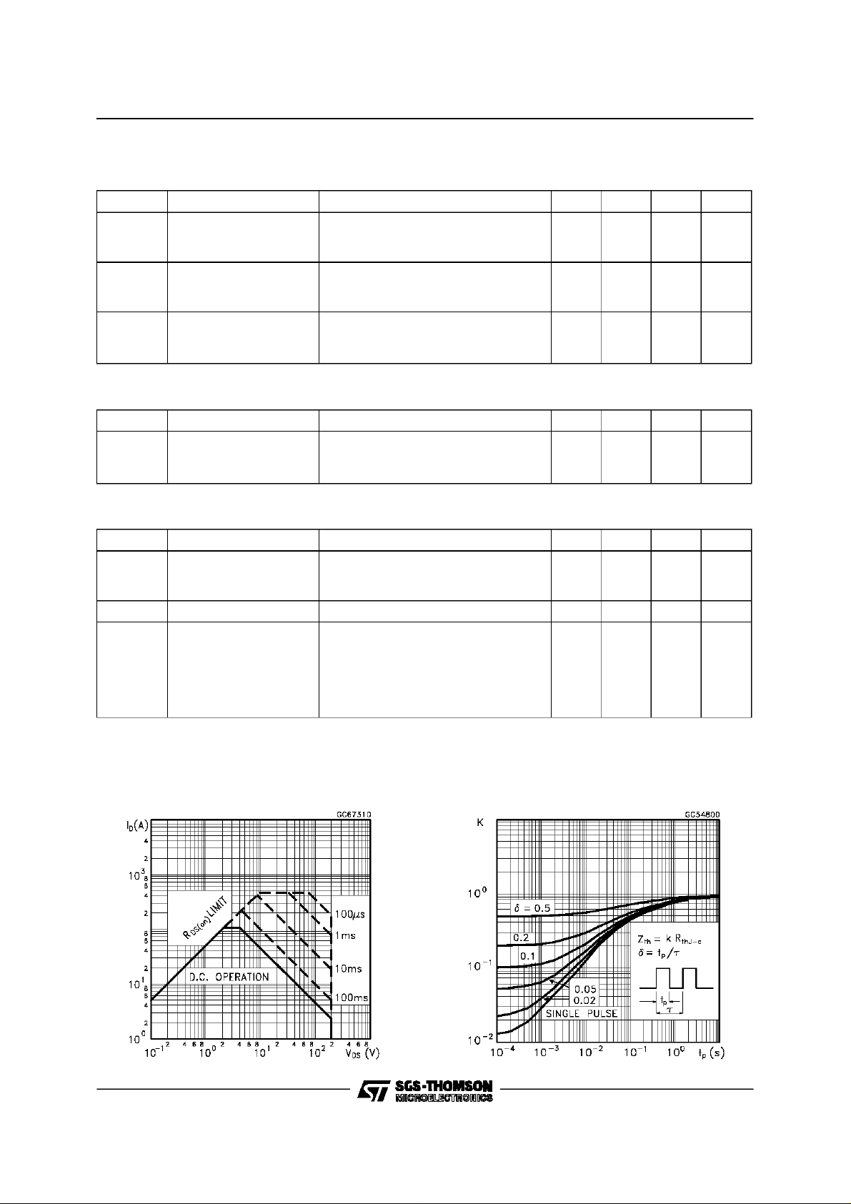
Safe Operating Area ThermalImpedance
A
A
ns
µC
A
3/8

STE110NA20
Derating Curve
TransferCharacteristics
OutputCharacteristics
Transconductance
StaticDrain-source On Resistance
4/8
Gate Charge vs Gate-source Voltage

STE110NA20
CapacitanceVariations
Normalized OnResistance vs Temperature
Normalized GateThreshold Voltage vs
Temperature
Turn-onCurrent Slope
Turn-offDrain-source VoltageSlope
Cross-overTime
5/8

STE110NA20
SwitchingSafe Operating Area
Source-drainDiode Forward Characteristics
AccidentalOverload Area
Fig. 1: UnclampedInductive Load Test Circuit
6/8
Fig. 2: UnclampedInductive Waveform

STE110NA20
Fig. 3: SwitchingTimes Test Circuits For
ResistiveLoad
Fig. 5: Test CircuitFor Inductive Load Switching
And DIodeRecovery Times
Fig. 4: GateCharge test Circuit
7/8

STE110NA20
Information furnished is believedto be accurateand reliable. However, SGS-THOMSON Microelectronics assumes no responsability for the
consequencesof use ofsuch informationnor for any infringement of patents or otherrights of third parties which may resultsfrom its use. No
licenseis grantedby implicationor otherwise underany patentor patentrights ofSGS-THOMSONMicroelectronics. Specificationsmentioned
in this publicationare subject to change without notice.This publication supersedes andreplaces all informationpreviously supplied.
SGS-THOMSONMicroelectronics products are notauthorized for useas criticalcomponents in lifesupportdevicesor systems withoutexpress
writtenapproval of SGS-THOMSONMicroelectonics.
1995 SGS-THOMSONMicroelectronics - All Rights Reserved
Australia - Brazil- France - Germany - HongKong - Italy- Japan- Korea - Malaysia - Malta - Morocco- The Netherlands -
Singapore- Spain- Sweden - Switzerland- Taiwan - Thailand - United Kingdom- U.S.A
SGS-THOMSONMicroelectronicsGROUPOF COMPANIES
...
8/8
 Loading...