

y
y
y
g
y
查询STE10/100供应商
PCI 10/100 ETHERNET CONTROLLER
1.0 DESCRIPTION
The STE10/100 is a high performance PCI Fast Ethernet controller with integrated physical layer interface for 10BASE-T and 100BASE-TX application.
It was designed with advanced CMOS technology to
provide glueless 32-bit bus master interface for PCI
bus, boot ROM interface, CSMA/CD protocol for Fast
Ethernet, as well as the physical media interface for
100BASE-TX of IEEE802.3u and 10BASE-T of
IEEE802.3. The auto-negotiation function is also
supported for speed and duplex detection.
The STE10/100 provides both half-duplex and fullduplex operation, as well as support for full-duplex
flow control. It provides long FIFO buffers for transmission and receiving, and early interrupt mechanism to enhance performance. The STE10/100 also
supports ACPI and PCI compliant power management function.
2.0 FEATURES
2.1 Industry standard
■
IEEE802.3u 100BASE-TX and IEEE802.3
10BASE-T comp l ia n t
■
Support for IEEE802.3x flow control
■
IEEE802.3u Auto-Negotiation support for
10BASE-T and 100BASE-TX
STE10/100
WITH INTEGRATED PHY (5V)
PRODUCT PREVIEW
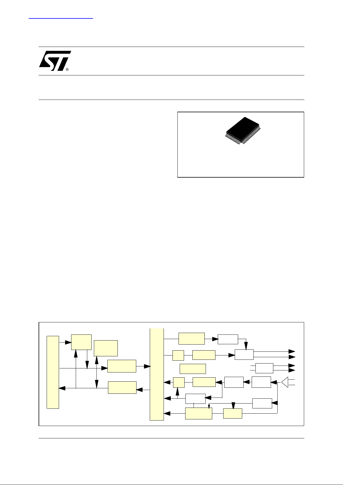
PQFP128 (14x20x2.7mm)
ORDERING NUMB ER: STE1 0/100
■
PCI bus interface Rev. 2.2 compliant
■
ACPI and PCI power management standard
compliant
■
Support PC99 wake on LAN
2.2 FIFO
■
Provides independent transmission and
receiving FIFOs, each 2k bytes long
■
Pre- fe tches u p to tw o trans mit pack e ts to
minimize inter frame gap (IFG) to 0.96us
■
Retransmits collided packet without reload from
host memory within 64 bytes.
■
Automatically retransmits FIFO under-run
packet with maximum drain threshold until 3rd
time retry failure without influencing the
registers and transmit threshold of next packet.
Figure 1. STE10/100Block Diagram
4B/5B
5B/4B
Manchester
Encoder
Auto
otiation
Ne
Descrambler
Scrambler
Flow
Control
DMA
Tx FiFo
MII
Controller
Rx FiFo
PCI Controller
M AC SubLaye
MI I Co n tr o ller
September 1999
This is preliminary information on a new product now in development. Details are subject to change without notice.
100 clock
Re cover
Manchester
Decoder
10 TX
Filter
BaseLine
Restore
Link
Polarit
Transmitter
25Mhz
TX Freq.
nth.
S
Adaptive
Equalization
10 clock
Re cover
125Mhz
20Mhz
+
_
1/66

STE10/100
2.3 PCI I/F
■
Provides 32-bit PCI bus master data transfer
■
Supports PCI clock with frequency from 0Hz to 33MHz
■
Supports network operation with PCI system clock from 20MHz to 33MHz
■
Provides performance meter and PCI bus master latency timer for tuning the threshold to enhance the
performance
■
Provides burst transmit packet interrupt and transmit/receive early interrupt to reduce host CPU
utilizatio n
■
As bus master, supports memory-read, memory-read-line, memory-read-multiple, memory-write,
memory-write-and-invalidate command
■
Supports big or little endian byte ordering
2.4 EEPROM/Boot ROM I/F
■
Provides writeable Flash ROM and EPROM as boot ROM, up to 128kB
■
Provides PCI to access boot ROM by byte, word, or double word
■
Re-writes Flash boot ROM through I/O port by programming register
■
Provides serial interface for read/write 93C46 EEPROM
■
Automatically loads device ID, vendor ID, subsystem ID, subsystem vendor ID, Maximum-Latency , and
Minimum-Grand from the 64 byte contents of 93C46 after PCI reset de-asserted
2.5 MAC/Physical
■
Integrates the complete set of Physical layer 100BASE-TX and 10BASE-T functions
■
Provides Full-duplex operation in both 100Mbps and 10Mb ps modes
■
Provides Auto-negotiation (NWAY) function of full/half duplex operation for both 10 and 100 Mbps
■
Provides MLT-3 transceiver with DC restoration for Base-line wander compensation
■
Provides transmit wave-shaper, receive filters, and adaptive equalizer
■
Provides MAC and Transceiver (TXCVR) loop-back modes for diagnostic
■
Built-in Stream Cipher Scrambler/ De-scrambler and 4B/5B encoder/decoder
■
Supports external transmit transformer with 1.414:1 turn ratio
■
Supports external receive transformer with 1:1 turn ratio
2.6 LED Display
■
Provides 2 LED display modes:
3 LED displays for
100Mbps (on) or 10Mbps (off)
Link (Remains on when link ok) or Activity (Blinks at 10Hz when receiving or transmitting collision-free)
FD (Remains on when in Full duplex mode) or when collision detected (Blinks at 20Hz)
4 LED displays for
100 Link (On when 100M link ok)
10 Link (On when 10M link ok)
Activity (Blinks at 10Hz when receiving or transmitting)
FD (Remains on when in Full duplex mode) or when collision detected (Blinks at 20Hz)
2/66
STE10/100
2.7 Miscellaneous
■
ACPI and PCI compliant power management functions offer significant power-savings performance
■
Provides general purpose timers
■
128-pin QFP package
Figure 2. System Diagram of the STE10/100
PCI
Interface
Serial
EEPROM
LEDs
Boot ROM
STE10/ 100
Xfmr Medium
25 MHz
Crystal
3/66

STE10/100
3.0 PIN ASSIGNEMENT DIAGRAM
Figure 3. Pin Connection
AD-25
AD-24
C-BEB3
IDSEL
-PCI
V
SS
AD-23
AD-22
-PCI
V
DD
AD-21
AD-20
V
-PCI
SS
AD-19
AD-18
-PCI
V
DD
AD-17
C-BEB2
FRAME#
-PCI
V
SS
IRDY#
TRDY#
DEVSEL#
STOP#
SERR#
PAR
-PCI
V
DD
C-BEB1
AD-15
AD-14
-PCI
V
SS
AD-11
AD-10
V
-PCI
SS
AD-9
-IR
DD
-PCI
DD
V
127
128
1
2
3
4
5
6
7
8
9
10
11
12
13
14
15
16AD-16
17
18
19
20
21
22
23
24PERR#
25
26
27
28
29
30
31
32AD-13
33AD-12
34
35
36
37
38V
39 40 41 42
AD-26
126
-PCI
DD
AD-30
AD-31
AD-28
AD-29
V
PME#
123122121120 118119 117116115114113
44 45 46 47 48
49 50
AD-27
125
-PCI
SS
V
124
43
REQ#
-PCI
SS
GNT#
PCI-CLK
V
51
52 53 54 55 56
T
-IR
-IR
SS
SS
INTA#
DD
V
AV
TX-
V
RST#
112 110111 109108107106105
59 60 61 62 63 64
57 58
T
DD
AV
TX+
R
AV
SS
RX+
104103
RX-
R
DD
AV
102
101
100
99
98
97
96
95
94
93
92
91
90
89
88
87
86
85
84
83
82
81
80
79
78
77
76
75
74
73
72
71
70
69
68
67
66
65
I
AV
SS
I
REF
AVDDI
AV
X
DD
X1
X2
AVSSX
REC
AV
DD
REC
AV
SS
V
-IR
SS
LED M1/M2
LED M1/M2
LED M1/M2
-detect
V
CC
-detect
V
CC
BrA-16/LED M2
BrA-15
-IR
V
DD
BrA-14
BrA-13
BrA-12
BrA-11
BrA-10
BrWE#
BrOE#
BrCS#
EECS
-IR
V
SS
BrD-7/ECK
BrD-6/EDI
BrD-5/EDO
BrD-4
BrD-3
BrD-2
BrD-1
BrD-0
BrA-9
BrA-8
4/66
-IR
SS
V
-PCI
DD
V
AD-8
AD-7
C-BEB0
AD-6
-PCI
SS
V
AD-5
AD-4
-PCI
DD
V
AD-3
AD-2
-PCI
SS
V
AD-1
AD-0
N.C.
-IR
SS
V
BrA -0
BrA-1
BrA-2
BrA-3
-IR
DD
V
BrA-4
BrA-5
BrA6
BrA-7
D99TL443

STE10/100
4.0 4. PIN DESCRIPTION
Table 1. Pin Description
Pin No. Name Type Description
PCI bus Interface
113 INTA# O/D PCI interrupt request. STE10/100 asserts this signal when one of the interrupt
event is set.
114 RST# I PCI Reset signal to initialize the STE10/100. The RST signal should be asserted
for at least 100µs to ensure that the STE10/100 completes initialization. During
the reset period, all the output pins of STE10/100 will be placed in a highimpedance state and all the O/D pins are floated.
116 PCI-CLK I PCI clock input to STE10/100 for PCI Bus functions. The Bus signals are
synchronized relative to the rising edge of PCI-CLK PCI-CLK must operate at a
frequency in the range between 20MHz and 33MHz to ensure proper network
operation
117 GNT# I PCI Bus Granted. This signal indicates that the STE10/100 has been granted
ownership of the PCI Bus as a result of a Bus Request.
118 REQ# O PCI Bus Request. STE10/100 asserts this line when it needs access to the PCI
Bus.
119 PME# O
120,121
123,124
126,127
1,2
6,7
9,10
12,13
15,16
29,30
32~35
37
41
43,44
46,47
49,50
52,53
3
17
28
42
AD-31,30
AD-29,28
AD-27,26
AD-25,24
AD-23,22
AD-21,20
AD-19,18
AD-17,16
AD-15,14
AD-13~10
AD-9
AD-8
AD-7, 6
AD-5,4
AD-3,2
AD-1,0
C-BEB3
C-BEB2
C-BEB1
C-BEB0
The Power Management Event signal is an open drain, active low signal. The
OD
I/O Multiplexed PCI Bus address/data pins
I/O Bus command and byte enable
STE10/100 will assert PME# to indicate that a power management event has
occurred.
When WOL (bit 18 of CSR18) is set, the STE10/100 is placed in Wake On LAN
mode. While in this mode, the STE10/100 will activate the PME# signal upon
receipt of a Magic Packet frame from the network.
In the Wake On LAN mode, when LWS (bit 17 of CSR18) is set, the LAN-WAKE
signal follows HP’s protocol; otherwise, it is IBM protocol.
4 IDSEL I Initialization Device Select. This signal is asserted when the host issues
configuration cycles to the STE10/100.
18 FRAME# I/O Asserted by PCI Bus master during bus tenure
20 IRDY# I/O Master device is ready to begin data transaction
5/66

STE10/100
Table 1. Pin Description
Pin No. Name Type Description
21 TRDY# I/O Target device is ready to begin data transaction
22 DEVSEL# I/O Device select. Indicates that a PCI target device address has been decoded
23 STOP# I/O PCI target device request to the PCI master to stop the current transaction
24 PERR# I/O Data parity error detected, driven by the device receiving data
25 SERR# O/D Address parity error
26 PAR I/O Parity. Even parity computed for AD[31:0] and C/BE[3:0]; master drives PAR for
address and write data phase, target drives PAR for read data phase
BootROM/EEPROM Interf ace
56~59
61~66
80~86
87
67~71
72
73
74
76 EECS O Chip Select of serial EEPROM
77 BrCS# O BootROM Chip Select
78 BrOE# O BootROM Read Output Enable for flash ROM application
79 BrWE# O BootROM Write Enable for flash ROM application.
Physical Interface
98 X1 I 25 MHz reference clock input for Physical portion. When an external 25 MHz
97 X2 O 25 MHz reference clock output for Physical portion. When an external 25MHz
BrA0~3
BrA4~9
BrA10~15
BrA16/
LED M2 -
Fd/Col
BrD0~4
BrD5/EDO
BrD6/EDI
BrD7/ECK
I/O ROM data bus
Provides up to 128kB EPROM or Flash-ROM application space.
This pin can be programmed as mode 2 LED display for Full Duplex or Collision
status. It will be driven (LED on) continually when a full duplex configuration is
detected, or it will be driven at a 20 Hz blinking frequency when a collision status
is detected in the half duplex configuration.
O
O/I
O/O
O/O
BootROM data bus (0~7)
EDO: Data output of serial EEPROM, data input to STE10/100
EDI:Data input to serial EEPROM, data output from STE10/100
ECK:Clock input to serial EEPROM, sourced by STE10/100
crystal is used, this pin will be connected to one of its terminals, and X2 will be
connected to the other terminal. If an external 25 MHz oscillator is used, then this
pin will be connected to the oscillator’s output pin.
crystal is used, this pin will be connected to one of the crystal terminals (see X1,
above). If an external clock source is used, then this pin should be left open.
107,109 TX+, TX- O The differential Transmit outputs of 100BASE-TX or 10BASE-T, these pins
105,104 RX+, RX- I The differential Receive inputs of 100BASE-TX or 10BASE-T, these pins connect
101 Iref O Reference Resistor connecting pin for reference current, directly connects a 5K
6/66
connect directly to Magnetic.
directly from Magnetic.
Ohm ± 1% resistor to Vss.

Table 1. Pin Description
Pin No. Name Type Description
LED display & Miscellaneous
STE10/100
90 LED M1-
LK/Act
or
LED M2-
Act
92 LED M1-
Speed
or
LED M2-
100 Link
91 LED M1-
Fd/Col
or
LED M2-
10 Link
89 Vaux-
detect
O This pin can be programmed as mode 1 or mode 2:
For mode 1:
LED display for Link and Activity status. This pin will be driven on continually
when a good Link test is detected. This pin will be driven at a 10 Hz blinking
frequency when either effective receiving or transmitting is detected.
For mode 2:
LED display for Activity status. This pin will be driven at a 10 Hz blinking
frequency when either effective receiving or transmitting is detected.
O This pin can be programmed as mode 1 or mode 2:
For mode 1:
LED display for 100M b/s or 10M b/s speed. This pin will be driven on continually
when the 100M b/s network operating speed is detected.
For mode 2:
LED display for 100Ms/s link status. This pin will be driven on continually when
100Mb/s network operating spped is detected.
O This pin can be programmed as mode 1 or mode 2:
For mode 1:
LED display for Full Duplex or Collision status. This pin will be driven on
continually when a full duplex configuration is detected. This pin will be driven at
a 20 Hz blinking frequency when a collision status is detected in the half duplex
configuration.
For mode 2:
LED display for 10Ms/s link status. This pin will be driven on continually when
10Mb/s network operating speed is detected.
I When this pin is asserted, it indicates an auxiliary power source is supported
from the system.
88 Vcc-detect I When this pin is asserted, it indicates a PCI power source is supported.
Digital Power Pins
5,11,19,31,36,39,45,51,55,75,93,112,115,125 Vss
8,14,27,38,40,48,60,85,111,122,128 Vdd
Analog Power Pins
94,96,102,106,110 AVss
95,99,100,103,108 AVdd
7/66

STE10/100
5.0 REGISTERS AND DESCRIPTORS DESCRIPTION
There are three kinds of registers within the STE10/100: STE10/100 configuration registers, PCI control/status
registers, and Transceiver control/status registers.
The STE10/100 configuration registers are used to initialize and configure the STE10/100 and for identifying
and querying the STE10/100.
The PCI control/status registers are used to communicate between the host and STE10/100. The host can initialize, control, and read the status of the STE10/100 through mapped I/O or memory address space.
The STE10/100 contains 11 16-bit registers to supported Transceiver control and status. They include 7 basic
registers which are defined ac cording to cl ause 22 “ Reconcili ation S ub-layer and Media Ind ependent Inter face”
and clause 28 “Physical Layer link signaling for 10 Mb/s and 100 Mb/s Auto-Negotiation on twisted pair” of the
IEEE802.3u standard. In addition, 4 special registers are provided for advanced chip control and status.
The STE10/100 also provides receive and transmit descriptors for packet buffering and management.
5.1 STE10/100 Configuration Registers
An STE10/100 software driver can initialize and configure the chip by writing its configuration registers. The
contents of configuration registers are set to their default values upon power-up or whenever a hardware reset
occurs, but their settings remain unchanged whenever a software reset occurs. The configuration registers are
byte, word, and double word accessible.
Table 2. STE10/100 configuration registers list
Offset I ndex Name Descriptions
00h CR0 LID Loaded device ID and vendor ID
04h CR1 CSC Configuration Status and Command
08h CR2 CC Class Code and revision number
0ch CR3 LT Latency Timer
10h CR4 IOBA IO Base Address
14h CR5 MBA Memory Base Address
2ch CR11 SID Subsystem ID and vendor ID
30h CR12 BRBA Boot ROM Base Address (ROM size = 128KB)
34h CR13 CP Capability Pointer
3ch CR15 CINT Configuration Interrup t
40h CR16 DS driver space for special purpose
80h CR32 SIG Signature of STE10/100
c0h CR48 PMR0 Power Management Register 0
c4h CR49 PMR1 Power Management Register 1
8/66

STE10/100
Table 3. STE10/100 configuration registers table
offset b31 ----------- b16 b15 ---------- b0
00h Device ID* Vendor ID*
04h Status Command
08h Base Class Code Subclass ------ Revision # Step #
0ch ------ ------ Latency timer cache line size
10h Base I/O address
14h Base memory address
18h~
28h
2ch Subsystem ID* Subsystem vendor ID*
30h Boot ROM base address
34h Reserved Cap_Ptr
38h Reserved
3ch Max_Lat* Min_Gnt* Interrupt pin Interrupt line
40
h Reserved Driver Space Reserved
Reserved
80h Signature of STE10/100
c0h PMC Next_Item_Ptr Cap_ID
c4h
Note: * : automatically recalled from EEPROM when PCI reset is deserted
DS(40h), bit15-8, is read/write able register
SIG(80h) is hard wired register, read only
Reserved
PMCSR
5.1.1 STE10/100 configuration registers des cri ptions
Table 4. Configuration Registers Descriptions
Bit # N ame Descriptions Default Va l RW Type
CR0(offset = 00h), LID - Loaded Identification number of Device and Vendor
31~16 LDID Loaded Device ID, the device ID number loaded from serial
EEPROM.
15~0 LVID Loaded Vendor ID, the vendor ID number loaded from serial
EEPROM.
From EEPROM: Loaded from EEPROM
CR1(offset = 04h), CSC - Configuration command and status
31 SPE Status Parity Error.
1: means that STE10/100 detected a parity error. This bit will
be set even if the parity error response (bit 6 of CR1) is
disabled.
From
EEPROM
From
EEPROM
0 R/W
R/O
R/O
30 SES Status System Error.
1: means that STE10/100 asserted the system error pin.
0 R/W
9/66

STE10/100
Table 4. Configuration Registers Descriptions
Bit # N ame Descriptions Default Va l RW Type
29 SMA Status Master Abort.
1: means that STE10/100 received a master abort and has
terminated a master transaction.
28 STA Status Target Abort.
1: means that STE10/100 received a target abort and has
terminated a master transaction.
27 --- Reserved.
26, 25 SDST Status Device Select Timing. Indicates the timing of the chip’s
assertion of device select.
01: indicates a medium assertion of DEVSEL#
24 SDPR Status Data Parity Report.
1: when three conditions are met:
a. STE10/100 asserted parity error (PERR#) or it detected
parity error asserted by another device.
b. STE10/100 is operating as a bus master.
c. STE10/100’s parity error response bit (bit 6 of CR1) is
enabled.
23 SFBB Status Fast Back-to-Back
Always 1, since STE10/100 has the ability to accept fast back
to back transactions.
22~21 --- Reserved.
20 NC New Capabilities. Indicates whether the STE10/100 provides a
list of extended capabilities, such as PCI power management.
1: the STE10/100 provides the PCI management function
0: the STE10/100 doesn’t provide New Capabilities.
0 R/W
0 R/W
01 R/O
0 R/W
1 R/O
Same as
bit 19 of
CSR18
RO
19~ 9 --- Reserved.
8 CSE Command System Error Response
1: enable system error response. The STE10/100 will assert
SERR# when it finds a parity error during the address phase.
7 --- Reserved.
6 CPE Command Parity Error Response
0: disable parity error response. STE10/100 will ignore any
detected parity error and keep on operating. Default value is
0.
1: enable parity error response. STE10/100 will assert system
error (bit 13 of CSR5) when a parity error is detected.
5~ 3 --- Reserved.
2 CMO Command Master Operation Ability
0: disable the STE10/100 bus master ability.
1: enable the PCI bus master ability. Default value is 1 for
normal operation.
1 CMSA Command Memory Space Access
0: disable the memory space access ability.
1: enable the memory space access ability.
0 R/W
0 R/W
0 R/W
0 R/W
10/66

STE10/100
Table 4. Configuration Registers Descriptions
Bit # N ame Descriptions Default Va l RW Type
0 CIOSA Command I/O Space Access
R/W: Read and Write able. RO: Read abl e o n ly.
CR2(offset = 08h), CC - Class Code and Revision Number
31~24 BCC Base Class Code. It means STE10/100 is a network controller. 02h RO
23~16 SC Subclass Code. It means STE10/100 is a Fast Ethernet
15~ 8 --- Reserved.
7 ~ 4 RN Revision Number, identifies the revision number of STE10/
3 ~ 0 SN Step Number, identifies the STE10/100 steps within the
RO: Read Only.
CR3(offset = 0ch), LT - Latency Timer
31~16 --- Reserved.
15~ 8 LT Latency Timer. This value specifies the latency timer of the
0: enable the I/O space access ability.
1: disable the I/O space access ability.
Controller.
100.
current revision.
STE10/100
asserts FRAME#, the latency timer starts to count. If the
latency timer expires and the STE10/100 is still asserting
FRAME#, the STE10/100 will terminate the data transaction
as soon as its GNT# is removed.
in units of PCI bus clock cycles. Once the STE10/100
0 R/W
00h RO
Ah RO
1h RO
0 R/W
7 ~ 0 CLS Cache Line Size. This value specifies the system cache line
size in units of 32-bit double words(DW). The STE10/100
supports cache line sizes of 8, 16, or 32 DW. CLS is used by
the STE10/100 driver to program the cache alignment bits (bit
14 and 15 of CSR0) which are used for cache oriented PCI
commands, e.g., memory-read-line, memory-read-multiple,
and memory-write-and-invalidate.
CR4(offset = 10h), IOBA - I/O Base Address
31~ 7 IOBA I/O Base Address. This value indicate the base address of PCI
control and status register (CSR0~28), and Transceiver
registers (XR0~10)
6 ~ 1 --- reserved.
0 IOSI I/O Space Indicator.
1: means that the configuration registers map into I/O space.
CR5(offset = 14h), MBA - Memory Base Address
31~ 7 MBA Memory Base Address. This value indicate the base address
of PCI control and status register(CSR0~28), and Transceiver
registers(XR0~10)
6 ~ 1 --- reserved.
0 R/W
0 R/W
1RO
0 R/W
11/66

STE10/100
Table 4. Configuration Registers Descriptions
Bit # N ame Descriptions Default Va l RW Type
0 IOSI Memory Space Indicator.
1: means that the configuration registers map into I/O space.
CR11(offset = 2ch), SID - Subsystem ID.
31~16 SID Subsystem ID. This value is loaded from EEPROM as a result
of power-on or hardware reset.
15~ 0 SVID Subsystem Vendor ID. This value is loaded from EEPROM as
a result power-on or hardware reset.
CR12(offset = 30h), BRBA - Boot ROM Base Address. This register should be initialized before accessing the
boot ROM space.
31~10 BRBA Boot ROM Base Address. This value indicates the address
mapping of the boot ROM field as well as defining the boot
ROM size. The values of bit 16~10 are set to 0 indicating that
the STE10/100 supports up to 128kB of boot ROM.
9 ~ 1 --- reserved RO R/W R/
0 BRE Boot ROM Enable. The STE10/100 will only enable its boot
ROM access if both the memory space access bit (bit 1 of
CR1) and this bit are set to 1.
1: enable Boot ROM. (if bit 1 of CR1 is also set)
CR13(offset = 34h), CP - Capabilities Pointer.
31~8 --- reserved
0RO
From
EEPROM
From
EEPROM
X: b31~17
0: b16~10
0 R/W
RO
RO
R/W
RO
W
7~0 CP Capabilities Pointer.
CR15(offset = 3ch), CI - Configuration Interrupt
31~24 ML Max_Lat register. This value indicates how often the STE10/
100 needs to access to the PCI bus in units of 250ns. This
value is loaded from serial EEPROM as a result of power-on or
hardware reset.
23~16 MG Min_Gnt register. This value indicates how long the STE10/
100 needs to retain the PCI bus ownership whenever it
initiates a transaction, in units of 250ns. This value is loaded
from serial EEPROM as a result power-on or hardware reset.
15~ 8 IP Interrupt Pin. This value indicates one of four interrupt request
pins to which the STE10/100 is connected.
01h: means the STE10/100 always connects to INTA#
7 ~ 0 IL Interrupt Line. This value indicates the system interrupt
request lines to which the INTA# of STE10/100 is routed. The
BIOS will fill this field when it initializes and configures the
system. The STE10/100 driver can use this value to determine
priority and vector information.
CR16(offset = 40h), DS - Driver Space for special purpose.
31~16 --- reserved
C0H RO
From
EEPROM
From
EEPROM
01h RO
0 R/W
RO
RO
12/66

STE10/100
Table 4. Configuration Registers Descriptions
Bit # N ame Descriptions Default Va l RW Type
15~8 DS Driver Space for implementation-specific purpose. Since this
7 ~ 0 --- reserved
CR32(offset = 80h), SIG - Signature of STE10/100
31~16 DID Device ID, the device ID number of the STE10/100. 0981h RO
15~0 VID Vendor ID 1317h RO
CR48(offset = c0h), PMR0, Power Management Register0.
31
30
29
28
27
26 D2S D2_Support. The STE10/100 supports the D2 Power
25 D1S D1_Support. The STE10/100 supports the D1 Power
PSD3c,
PSD3h,
PSD2,
PSD1,
PSD0
area won’t be cleared upon software reset, an STE10/100
driver can use this R/W area as user-specified storage.
PME_Support.
The STE10/100 will assert PME# signal while in the D0, D1,
D2, D3hot and D3cold power state. The STE10/100 supports
Wake-up from the above five states. Bit 31 (support wake-up
from D3cold) is loaded from EEPROM after power-up or
hardware reset. To support the D3cold wake-up function, an
auxiliary power source will be sensed during reset by the
STE10/100 Vaux_detect pin. If sensed low, PSD3c will be set
to 0; if sensed high, and if D3CS (bit 31of CSR18) is set
(CSR18 bits 16~31 are recalled from EEPROM at reset), then
bit 31 will be set to 1.
Management State.
Management State.
0 R/W
X1111b RO
1RO
1RO
24~22 AUXC Aux Current. These three bits report the maximum 3.3Vaux
current requirements for STE10/100 chip. If bit 31 of PMR0 is
‘1’, the default value is 111b, meaning the STE10/100 needs
375 mA to support remote wake-up in D3cold power state.
Otherwise, the default value is 000b, meaning the STE10/100
does not support remote wake-up from D3cold power state.
21 DSI The Device Specific Initialization bit indicates whether any
special initialization of this function is required before the
generic class device driver is able to use it.
0: indicates that the function does not require a device-specific
initialization sequence following transition to the D0
uninitialized state.
20 --- Reserved.
19 PMEC PME Clock. Indicates that the STE10/100 does not rely on the
presence of the PCI clock for PME# operation
18~16 VER Version. The value of 010b indicates that the STE10/100
complies with Revision 1.0a of the PCI Power Management
Interface Specification.
15~8 NIP Next Item Pointer. This value is always 0h, indicating that
there are no additional items in the Capabilities List.
7~0 CAPID Capability Identifier. This value is always 01h, indicating the
link list item as being the PCI Power Management Registers.
XXXb RO
0RO
0RO
010b RO
00h RO
01h RO
13/66

STE10/100
Table 4. Configuration Registers Descriptions
Bit # N ame Descriptions Default Va l RW Type
CR49(offset = c4h), PMR1, Power Management Register 1.
31~16 --- reserved
15 PMEST PME_Status. This bit is set whenever the STE10/100 detects
a wake-up event, regardless of the state of the PME-En bit.
Writing a “1” to this bit will clear it, causing the STE10/100 to
deassert PME# (if so enabled). Writing a “0” has no effect.
If PSD3c (bit 31 of PMR0) is cleared (i.e. it does not support
PME# generation from D3cold), this bit is by default 0;
otherwise, PMEST is cleared upon power-up reset only and is
not modified by either hardware or software reset.
14,13 DSCAL Data_Scale. Indicates the scaling factor to be used when
interpreting the value of the Data register. This field is
required for any function that implements the Data register.
The STE10/100 does not support Data register and
Data_Scale.
12~9 DSEL Data_Select. This four bit field is used to select which data is
to be reported through the Data register and Data_Scale field.
This field is required for any function that implements the Data
register.
The STE10/100 does not support Data_select.
8 PME_En PME_En. When set, enables the STE10/100 to assert PME#.
When cleared, disables the PME# assertion.
If PSD3c (bit 31 of PMR0) is cleared (i.e. it does not support
PME# generation from D3cold), this bit is by default 0;
otherwise, PME_En is cleared upon power up reset only and is
not modified by either hardware or software reset.
7~2 --- reserved. 000000b RO
X R/W1C*
00b RO
0000b R/W
X R/W
1,0 PWRS PowerState. This two bit field is used both to determine the
current power state of the STE10/100 and to place the STE10/
100 in a new power state. The definition of this field is given
below.
00b - D0
01b - D1
10b - D2
11b - D3hot
If software attempts to write an unsupported state to this field,
the write operation will complete normally on the bus, but the
data is discarded and no state change occurs.
R/W1C*, Read Only and Wri te one cleare d.
14/66
00b R/W

5.2 PCI Control/Status registers
Table 5. PCI Control/Status registers list
offset from base
address of CSR
00h CSR0 PAR PCI access register
08h CSR1 TDR transmit demand register
10h CSR2 RDR receive demand register
18h CSR3 RDB receive descriptor base address
20h CSR4 TDB transmit descriptor base address
28h CSR5 SR status register
30h CSR6 NAR network access register
38h CSR7 IER interrupt enable register
40h CSR8 LPC lost packet counter
48h CSR9 SPR serial port register
Index Name Descriptions
STE10/100
50h CSR10 --- Reserved
58h CSR11 TMR Timer
60h CSR12 --- Reserved
68h CSR13 WCSR Wake-up Control/Status Register
70h CSR14 WPDR Wake-up Pattern Data Register
78h CSR15 WTMR watchdog timer
80h CSR16 ACSR5 status register 2
84h CSR17 ACSR7 interrupt enable register 2
88h CSR18 CR command register
8ch CSR19 PCIC PCI bus performanc e counter
90h CSR20 PMCSR Power Management Command and Status
94h CSR21 --- Reserved
98h CSR22 --- Reserved
9ch CSR23 TXBR transmit burst counter/time-out register
a0h CSR24 FROM flash(boot) ROM port
a4h CSR25 PAR0 physical address register 0
a8h CSR26 PAR1 physical address register 1
ach CSR27 MAR0 multicast address hash table register 0
b0h CSR28 MAR1 multicast address hash table register 1
15/66

STE10/100
Table 6. Control/Status register description
Bit # N ame Descriptions Default Va l RW Type
CSR0(offset = 00h), PAR - PCI Access Register
31~25 --- reserved
24 MWIE Memory Write and Invalidate Enable.
1: enable STE10/100 to generate memory write invalidate
command. The STE10/100 will generate this command
while writing full cache lines.
0: disable generating memory write invalidate command. The
STE10/100 will use memory write commands instead.
23 MRLE Memory Read Line Enable.
1: enable STE10/100 to generate memory read line command
when read access instruction reaches the cache line
boundary. If the read access instruction doesn’t reach the
cache line boundary then the STE10/100 uses the memory
read command instead.
22 --- reserved
21 MRME Memory Read Multiple Enable.
1: enable STE10/100 to generate memory read multiple
commands when reading a full cache line. If the memory is
not cache-aligned, the STE10/100 uses the memory read
command instead.
20~19 --- reserved
18,17 TAP Transmit auto-polling in transmit suspended state.
00: disable auto-polling (default)
01: polling own-bit every 200 us
10: polling own-bit every 800 us
11: polling own-bit every 1600 us
16 --- reserved
0 R/W*
0 R/W*
0 R/W*
00 R/W*
15, 14 CAL Cache alignment. Address boundary for data burst, set after
reset
00: reserved (default)
01: 8 DW boundary alignment
10: 16 DW boundary alignment
11: 32 DW boundary alignment
13 ~ 8 PBL Programmable Burst Length. This value defines the maximum
number of DW to be transferred in one DMA transaction.
value: 0 (unlimited), 1, 2, 4, 8, 16(default), 32
7 BLE Big or Little Endian selection.
0: little endian (e.g. INTEL)
1: big endian (only for data buffer)
6 ~ 2 DSL Descriptor Skip Length. Defines the gap between two
descriptors in the units of DW.
1 BAR Bus arbitration
0: receive operations have higher priority
1: transmit operations have higher priority
16/66
00 R/W*
010000 R/W*
0 R/W*
0 R/W*
0 R/W*

STE10/100
Table 6. Control/Status register description
Bit # N ame Descriptions Default Va l RW Type
0 SWR Software reset
0 R/W*
1: reset all internal hardware (including MAC and
transceivers), except configuration registers. This signal will be
cleared by the STE10/100 itself after the reset process is
completed.
R/W* = Before writing the transmit and receive operations should be stopped.
CSR1(offset = 08h), TDR - Transmit demand register
31~ 0 TPDM Transmit poll demand.
While the STE10/100 is in the suspended state, a write to this
FFFFFFFF
h
register (any value) will trigger the read-tx-descriptor process,
which checks the own-bit; if set, the transmit process is then
started.
R/W* = Before writing the transmit process should be in the suspended state.
CSR2(offset = 10h), RDR - Receive demand register
31 ~ 0 RPDM Receive poll demand
While the STE10/100 is in the suspended state, a write to this
FFFFFFFF
h
register (any value) will trigger the read-rx-descriptor process,
which checks the own-bit, if set, the process to move data from
the FIFO to buffer is then started.
R/W* = Before writing the receive process should be in the suspended state.
CSR3(offset = 18h), RDB - Receive descriptor base address
31~ 2 SAR Start address of receive descriptor 0 R/W*
R/W*
R/W*
1, 0 RBND must be 00, DW boundary 00 RO
R/W* = Before writing the receive process should be stopped.
CSR4(offset = 20h), TDB - Transmit descriptor base address
31~ 2 SAT Start address of transmit descriptor 0 R/W*
1, 0 TBND must be 00, DW boundary 00 RO
R/W* = Before writing the transmit process should be stopped.
CSR5(offset = 28h), SR - Status register
31~ 26 ---- reserved
25~ 23 BET Bus Error Type. This field is valid only when bit 13 of
000 RO
CSR5(fatal bus error) is set. There is no interrupt generated by
this field.
000: parity error, 001: master abort, 010: target abort
011, 1xx: reserved
17/66

STE10/100
Table 6. Control/Status register description
Bit # N ame Descriptions Default Va l RW Type
22~ 20 TS Transmit State. Reports the current transmission state only, no
interrupt will be generated.
000: stop
001: read descriptor
010: transmitting
011: FIFO fill, read the data from memory and put into FIFO
100: reserved
101: reserved
110: suspended, unavailable transmit descriptor or FIFO
overflow
111: write descriptor
19~17 RS Receive State. Reports current receive state only, no interrupt
will be generated.
000: stop
001: read descriptor
010: check this packet and pre-fetch next descriptor
011: wait for receiving data
100: suspended
101: write descriptor
110: flush the current FIFO
111: FIFO drain, move data from receiving FIFO into memory
16 NISS Normal Interrupt Status Summary. Set if any of the following
bits of CSR5 are asserted:
TCI, transmit completed interrupt (bit 0)
TDU, transmit descriptor unavailable (bit 2)
RCI, receive completed interrupt (bit 6)
15 AISS Abnormal Interrupt Status Summary. Set if any of the following
bits of CSR5 are asserted:
TPS, transmit process stopped (bit 1)
TJT, transmit jabber timer time-out (bit 3)
TUF, transmit under-flow (bit 5)
RDU, receive descriptor unavailable (bit 7)
RPS, receive process stopped (bit 8)
RWT, receive watchdog time-out (bit 9)
GPTT, general purpose timer time-out (bit 11)
FBE, fatal bus error (bit 13)
000 RO
000 RO
0 RO/LH*
0 RO/LH*
14 ---- reserved
13 FBE Fatal Bus Error.
1: on occurrence of parity error, master abort, or target abort
(see bits 25~23 of CSR5). The STE10/100 will disable all bus
access. A software reset is required to recover from a parity
error.
12 --- reserved
11 GPTT General Purpose Timer Timeout, based on CSR11 timer
register
10 --- reserved
9 RWT Receive Watchdog Timeout, based on CSR15 watchdog timer
register
8 RPS Receive Process Stopped, receive state = stop 0 RO/LH*
18/66
0 RO/LH*
0 RO/LH*
0 RO/LH*

STE10/100
Table 6. Control/Status register description
Bit # N ame Descriptions Default Va l RW Type
7 RDU Receive Descriptor Unavailable
1: when the next receive descriptor can not be obtained by the
STE10/100. The receive process is suspended in this
situation. To restart the receive process, the ownership bit of
the next receive descriptor should be set to STE10/100 and a
receive poll demand command should be issued (if the receive
poll demand is not issued, the receive process will resume
when a new recognized frame is received).
6 RCI Receive Completed Interrupt
1: when a frame reception is completed.
5 TUF Transmit Under-Flow
1: when an under-flow condition occurs in the transmit FIFO
during transmitting. The transmit process will enter the
suspended state and report the under-flow errror on bit 1 of
TDES0.
4 --- Reserved
3 TJT Transmit Jabber Timer Time-out
1: when the transmit jabber timer expires. The transmit
processor will enter the stop state and TO (bit 14 of TDES0,
transmit jabber time-out flag) will be asserted.
2 TDU Transmit Descriptor Unavailable
1: when the next transmit descriptor can not be obtained by
the STE10/100. The transmission process is suspended in this
situation. To restart the transmission process, the ownership
bit of the next transmit descriptor should be set to STE10/100
and, if the transmit automatic polling is not enabled, a transmit
poll demand command should then be issued.
0 RO/LH*
0 RO/LH*
0 RO/LH*
0 RO/LH*
0 RO/LH*
1 TPS Transmit Process Stopped.
1: while transmit state = stop
0 TCI Transmit Completed Interrupt.
1: set when a frame transmission completes with IC (bit 31 of
TDES1) asserted in the first transmit descriptor of the frame.
LH = High Latching and cleared by writing 1.
CSR6(offset = 30h), NAR - Network access register
31~22 --- reserved
21 SF Store and forward for transmit
0: disable
1: enable, ignore the transmit threshold setting
20 --- reserved
19 SQE SQE Disable
0: enable SQE function for 10BASE-T operation. The STE10/
100 provides SQE test function for 10BASE-T half duplex
operation.
1: disable SQE function.
18~16 ----- reserved
0 RO/LH*
0 RO/LH*
0 R/W*
1 R/W*
19/66

STE10/100
Table 6. Control/Status register description
Bit # N ame Descriptions Default Va l RW Type
15~14 TR transmit threshold control
00: 128-bytes (100Mbps), 72-bytes (10Mbps)
01: 256-bytes (100Mbps), 96-bytes (10Mbps)
10: 512-bytes (100Mbps), 128-bytes (10Mbps)
11: 1024-bytes (100Mbps), 160-bytes (10Mbps)
13 ST Stop transmit
0: stop (default)
1: start
12 FC Force collision mode
0: disable
1: generate collision upon transmit (for testing in loop-back
mode)
11, 10 OM Operating Mode
00: normal
01: MAC loop-back, regardless of contents of XLBEN (bit 14 of
XR0, XCVR loop-back)
10,11: reser ved
9, 8 --- reserved
7 MM Multicast Mode
1: receive all multicast packets
6 PR Promiscuous Mode
1: receive any good packet.
0: receive only the right destination address packets
5 SBC Stop Back-off Counter
1: back-off counter stops when carrier is active, and resumes
when carrier is dropped.
0: back-off counter is not effected by carrier
00 R/W*
0 R/W
0 R/W**
00 R/W**
0 R/W***
1 R/W***
0 R/W**
4 --- reserved
3 PB Pass Bad packet
1: receives any packets passing address filter, including runt
packets, CRC error, truncated packets. For receiving all
bad packets, PR (bit 6 of CSR6) should be set to 1.
0: filters all bad packets
2 --- reserved
1 SR Start/Stop Receive
0: receive processor will enter stop state after the current
frame reception is completed. This value is effective only
when the receive processor is in the running or suspending
state. Note: In “Stop Receive” state, the PA USE packet and
Remote Wake Up packet will not be affected and can be
received if the corresponding function is enabled.
1: receive processor will enter running state.
0 --- reserved
W* = only write when the transmit processor stopped.
W** = only write when the transmit and rece ive processor both stopped.
W*** = only write when the receive processor stopped.
CSR7(offset = 38h), IER - Interrupt Enable Register
20/66
0 R/W***
0 R/W

STE10/100
Table 6. Control/Status register description
Bit # N ame Descriptions Default Va l RW Type
31~17 --- reserved
16 NIE Normal Interrupt Enable
1: enables all the normal interrupt bits (see bit 16 of CSR5)
15 AIE Abnormal Interrupt Enable
1: enables all the abnormal interrupt bits (see bit 15 of CSR5)
14 --- reserved
13 FBEIE Fatal Bus Error Interrupt Enable
1: this bit in conjunction with AIE (bit 15 of CSR7) will enable
the fatal bus error interrupt
12 --- Reserved
11 GPTIE General Purpose Timer Interrupt Enable
1: this bit in conjunction with AIE (bit 15 of CSR7) will enable
the general purpose timer expired interrupt.
10 --- Reserved
9 RWTIE Receive Watchdog Time-out Interrupt Enable
1: this bit in conjunction with AIE (bit 15 of CSR7) will enable
the receive watchdog time-out interrupt.
8 RSIE Receive Stopped Interrupt Enable
1: this bit in conjunction with AIE (bit 15 of CSR7) will enable
the receive stopped interrupt.
7 RUIE Receive Descriptor Unavailable Interrupt Enable
1: this bit in conjunction with AIE (bit 15 of CSR7) will enable
the receive descriptor unavailable interrupt.
0 R/W
0 R/W
0 R/W
0 R/W
0 R/W
0 R/W
0 R/W
6 RCIE Receive Completed Interrupt Enable
1: this bit in conjunction with NIE (bit 16 of CSR7) will enable
the receive completed interrupt.
5 TUIE Transmit Under-flow Interrupt Enable
1: this bit in conjunction with AIE (bit 15 of CSR7) will enable
the transmit under-flow interrupt.
4 --- Reserved
3 TJTTIE Transmit Jabber Timer Time-out Interrupt Enable
1: this bit in conjunction with AIE (bit 15 of CSR7) will enable
the transmit jabber timer time-out interrupt.
2 TDUIE Transmit Descriptor Unavailable Interrupt Enable
1: this bit in conjunction with NIE (bit 16 of CSR7) will enable
the transmit descriptor unavailable interrupt.
1 TPSIE Transmit Processor Stopped Interrupt Enable
1: this bit in conjunction with AIE (bit 15 of CSR7) will enable
the transmit processor stopped interrupt.
0 TCIE Transmit Completed Interrupt Enable
1: this bit in conjunction with NIE (bit 16 of CSR7) will enable
the transmit completed interrupt.
CSR8(offset = 40h), LPC - Lost packet counter
0 R/W
0 R/W
0 R/W
0 R/W
0 R/W
0 R/W
21/66

STE10/100
Table 6. Control/Status register description
Bit # N ame Descriptions Default Va l RW Type
31~17 --- Reserved
16 LPCO Lost Packet Counter Overflow
1: when lost packet counter overflow occurs. Cleared after
read.
15~0 LPC Lost Packet Counter
The counter is incremented whenever a packet is discarded as
a result of no host receive descriptors being available. Cleared
after read.
CSR9(offset = 48h), SPR - Serial port register
31~15 --- Reserved
14 SRC Serial EEPROM Read Control
When set, enables read access from EEPROM, when SRS
(CSR9 bit 11) is also set.
13 SWC Serial EEPROM Write Control
When set, enables write access to EEPROM, when SRS
(CSR9 bit 11) is also set.
12 --- Reserved
11 SRS Serial EEPROM Select
When set, enables access to the serial EEPROM (see
description of CSR9 bit 14 and CSR9 bit 13)
10~4 --- Reserved
3 SDO Serial EEPROM data out
This bit serially shifts data from the EEPROM to the STE10/
100.
0 RO/LH
0 RO/LH
0 R/W
0 R/W
0 R/W
1RO
2 SDI Serial EEPROM data in
This bit serially shifts data from the STE10/100 to the
EEPROM.
1 SCLK Serial EEPROM clock
High/Low this bit to provide the clock signal for EEPROM.
0 SCS Serial EEPROM chip select
1: selects the serial EEPROM chip.
CSR11(offset = 58h), TMR -General-purpose Timer
31~17 --- Reserved
16 COM Continuous Operation Mode
1: sets the general-purpose timer in continuous operating
mode.
15~0 GTV General-purpose Timer Value
Sets the counter value. This is a count-down counter with a
cycle time of 204us.
CSR13(offset = 68h), WCSR –Wake-up Control/Status Register
31 --- Reserved
22/66
1 R/W
1 R/W
1 R/W
0 R/W
0 R/W

STE10/100
Table 6. Control/Status register description
Bit # N ame Descriptions Default Va l RW Type
30 CRCT CRC-16 Type
0: Initial contents = 0000h
1: Initial contents = FFFFh
29 WP1E Wake-up Pattern One Matched Enable. 0 R/W
28 WP2E Wake-up Pattern Two Matched Enable. 0 R/W
27 WP3E Wake-up Pattern Three Matched Enable. 0 R/W
26 WP4E Wake-up Pattern Four Matched Enable. 0 R/W
25 WP5E Wake-up Pattern Five Matched Enable. 0 R/W
24-18 --- Reserved
17 LinkOFF Link Off Detect Enable. The STE10/100 will set the LSC bit of
CSR13 after it has detected that link status has transitioned
from ON to OFF.
16 LinkON Link On Detect Enable. The STE10/100 will set the LSC bit of
CSR13 after it has detected that link status has transitioned
from OFF to ON.
15-11 --- Reserved
10 WFRE Wake-up Frame Received Enable. The STE10/100 will
include the “Wake-up Frame Received” event in its set of
wake-up events. If this bit is set, STE10/100 will assert
PMEST bit of PMR1 (CR49) after STE10/100 has received a
matched wake-up frame.
0 R/W
0 R/W
0 R/W
0 R/W
9 MPRE Magic Packet Received Enable. The STE10/100 will include
the “Magic Packet Received” event in its set of wake-up
events. If this bit is set, STE10/100 will assert PMEST bit of
PMR1 (CR49) after STE10/100 has received a Magic packet.
8 LSCE Link Status Changed Enable. The STE10/100 will include the
“Link Status Changed” event in its set of wake-up events. If
this bit is set, STE10/100 will assert PMEST bit of PMR1 after
STE10/100 has detected a link status changed event.
7-3 --- Reserved
2 WFR Wake-up Frame Received,
1: Indicates STE10/100 has received a wake-up frame. It is
cleared by writing a 1 or upon power-up reset. It is not
affected by a hardware or software reset.
1 MPR Magic Packet Received,
1: Indicates STE10/100 has received a magic packet. It is
cleared by writing a 1 or upon power-up reset. It is not
affected by a hardware or software reset.
0 LSC Link Status Changed,
1: Indicates STE10/100 has detected a link status change
event. It is cleared by writing a 1 or upon power-up reset. It
is not affected by a hardware or software reset.
R/W1C*, Read Only and Write one clea red .
Default 1 if
PM & WOL
bits of CSR
18 are both
enabled.
0 R/W
X R/W1C*
X R/W1C*
X R/W1C*
R/W
23/66

STE10/100
Table 6. Control/Status register description
CSR14(offset = 70h), WPDR –Wake-up Pattern Data Register
Offset 31 16 15 8 7 0
0000h Wake-up pattern 1 mask bits 31:0
0004h Wake-up pattern 1 mask bits 63:32
0008h Wake-up pattern 1 mask bits 95:64
000ch Wake-up pattern 1 mask bits 127:96
0010h CRC16 of pattern 1 Reserved Wake-up pattern 1 offset
0014h Wake-up pattern 2 mask bits 31:0
0018h Wake-up pattern 2 mask bits 63:32
001ch Wake-up pattern 2 mask bits 95:64
0020h Wake-up pattern 2 mask bits 127:96
0024h CRC16 of pattern 2 Reserved Wake-up pattern 2 offset
0028h Wake-up pattern 3 mask bits 31:0
002ch Wake-up pattern 3 mask bits 63:32
0030h Wake-up pattern 3 mask bits 95:64
0034h Wake-up pattern 3 mask bits 127:96
0038h CRC16 of pattern 3 Reserved Wake-up pattern 3 offset
003ch Wake-up pattern 4 mask bits 31:0
0040h Wake-up pattern 4 mask bits 63:32
0044h Wake-up pattern 4 mask bits 95:64
0048h Wake-up pattern 4 mask bits 127:96
004ch CRC16 of pattern 4 Reserved Wake-up pattern 4 offset
0050h Wake-up pattern 5 mask bits 31:0
0054h Wake-up pattern 5 mask bits 63:32
0058h Wake-up pattern 5 mask bits 95:64
005ch Wake-up pattern 5 mask bits 127:96
0060h CRC16 of pattern 5 Reserved Wake-up pattern 5 offset
1. Offset value is from 0-255 (8-bit width).
2. To load the whole wake-u p f ram e filterin g i nf ormation, consecutive 2 5 l ong words write operation t o CS R14 should be done.
24/66

STE10/100
Table 6. Control/Status register description
Bit # N ame Descriptions Default Va l RW Type
CSR15(offset = 78h), WTMR - Watchdog timer
31~6 --- Reserved
5 RWR Receive Watchdog Release. The time (in bit-times) from
sensing dropped carrier to releasing watchdog timer.
0: 24 bit-times
1: 48 bit-times
4 RWD Receive Watchdog Disable
0: If the received packet‘s length exceeds 2560 bytes, the
watchdog timer will expire.
1: disable the receive watchdog.
3 --- Reserved
2 J CLK Jabber clock
0: cut off transmission after 2.6 ms (100Mbps) or 26 ms
(10Mbps).
1: cut off transmission after 2560 byte-time.
1 NJ Non-Jabber
0: if jabber expires, re-enable transmit function after 42 ms
(100Mbps) or 420ms (10Mbps).
1: immediately re-enable the transmit function after jabber
expires.
0 JBD Jabber disable
1: disable transmit jabber function
CSR16(offset = 80h), ACSR5 - Assistant CSR5(Status register 2)
31 TEIS Transmit Early Interrupt status
Transmit early interrupt status is set to 1 when TEIE (bit 31 of
CSR17 set) is enabled and the transmitted packet is moved
from descriptors to the TX-FIFO buffer. This bit is cleared by
writing a 1.
0 R/W
0 R/W
0 R/W
0 R/W
0 R/W
0 RO/LH*
30 REIS Receive Early Interrupt Status.
Receive early interrupt status is set to 1 when REIE (CSR17
bit 30) is enabled and the received packet has filled up its first
receive descriptor. This bit is cleared by writing a 1.
29 XIS Transceiver (XCVR) Interrupt Status. Formed by the logical
OR of XR8 bits 6~0.
28 TDIS Transmit Deferred Interrupt Status. 0 RO/LH*
27 --- Reserved
26 PFR PAUSE Frame Received Interrupt Status
1: indicates receipt of a PAUSE frame while the PAUSE
function is enabled.
25~ 23 BET Bus Error Type. This field is valid only when FBE (CSR5 bit
13, fatal bus error) is set. There is no interrupt generated by
this field.
000: parity error, 001: master abort, 010: target abort
011, 1xx: reserved
0 RO/LH*
0 RO/LH*
0 RO/LH*
000 RO
25/66

STE10/100
Table 6. Control/Status register description
Bit # N ame Descriptions Default Va l RW Type
22~ 20 TS Transmit State. Reports the current transmission state only,
no interrupt will be generated.
000: stop
001: read descriptor
010: transmitting
011: FIFO fill, read the data from memory and put into FIFO
100: reserved
101: reserved
110: suspended, unavailable transmit descriptor or FIFO
overflow
111: write descriptor
19~17 RS Receive State. Reports current receive state only , no interrupt
will be generated.
000: stop
001: read descriptor
010: check this packet and pre-fetch next descriptor
011: wait for receiving data
100: suspended
101: write descriptor
110: flush the current FIFO
111: FIFO drain, move data from receiving FIFO into memory
16 ANISS Added normal interrupt status summary.
1: whenever any of the added normal interrupts occur.
15 AAISS Added Abnormal Interr upt Statu s Summary.
1: whenever any of the added abnormal interrupts occur.
14~0 These bits are the same as the status register of CSR5, and
are accessible through either CSR5 or CSR16.
000 RO
000 RO
0 RO/LH*
0 RO/LH*
LH* = High Latching and cleared by writing 1.
CSR17(offset = 84h), ACSR7- Assistant CSR7(Interrupt enable register 2)
31 TEIE Transmit Early Interrupt Enable 0 R/W
30 REIE Receive Early Interrupt Enable 0 R/W
29 XIE Transceiver (XCVR) Interrupt Enable 0 R/W
28 TDIE Transmit Deferred Interrupt Enable 0 R/W
27 --- Reserved
26 PFRIE PAUSE Frame Received Interrupt Enable 0 R/W
25~17 --- Reserved
16 ANISE Added Normal Interrupt Summary Enable.
1: adds the interrupts of bits 30 and 31 of ACSR7 (CSR17) to
the normal interrupt summary (bit 16 of CSR5).
15 A AIE Ad ded Abno r mal Interr upt Summ ar y Enable.
1: adds the interrupt of bits 27, 28, and 29 of ACSR7 (CSR17)
to the abnormal interrupt summary (bit 16 of CSR5).
14~0 These bits are the same as the interrupt enable register of
CSR7, and are accessible through either CSR7 or CSR16.
0 R/W
0 R/W
26/66

STE10/100
Table 6. Control/Status register description
Bit # N ame Descriptions Default Va l RW Type
CSR18(offset = 88h), CR - Command Register, bit31 to bit16 automatically recall from EEPROM
31 D3CS D3cold power state wake up Support. If this bit is reset then
bit 31 of PMR0 will be reset to ‘0’. If this bit is asserted and an
auxiliary power source is detected then bit 31 of PMR0 will be
set to ‘1’.
30-28 AUXCL Aux. Current Load. These three bits report the maximum
27-24 --- Reserved
23 4LEDmode
_on
22, 21 RFS Receive FIFO size control
3.3Vaux current requirements for STE10/100 chip. If bit 31 of
PMR0 is ‘1’, the default value is 111b, which means the
STE10/100 need 375 mA to support remote wake-up in
D3cold power state. Otherwise, the default value is 000b,
which means the STE10/100 does not support remote wakeup from D3cold power state.
This bit is used to control the LED mode selection.
If this bit is reset, mode 1 (3 LEDs) is selected; the LEDs
definition is:
100/10 speed
Link/Activity
Full Duplex/Collision
If this bit is set, mode 2 (4 LEDs) is selected; the LEDs
definition is:
100 Link
10 Link
Activity
Full Duplex/Collision
11: 1K bytes
10: 2K bytes
01,00: reser ved
0
from
EEPROM
000b
from
EEPROM
0
from
EEPROM
10
from
EEPROM
R/W
R/W
R/W
R/W
20 --- Re ser ved
19 PM Power Management. Enables the STE10/100 Power
Management abilities. When this bit is set into “0” the STE10/
100 will set the Cap_Ptr register to zero, indicating no PCI
compliant power management capabilities. The value of this
bit will be mapped to NC (CR1 bit 20). In PCI Power
Management mode, the Wake Up Frames include “Magic
Packet”, “Unicast”, and “Muliticast”.
18 WOL Wake on LAN mode enable. When this bit is set to ‘1’, then the
STE10/100 enters Wake On LAN mode and enters the sleep
state.
Once the STE10/100 enters the sleep state, it remains there
until: the Wake Up event occurs, the WOL bit is cleared, or a
reset (software or hardware) happens.
In Wake On LAN mode the Wake-Up frame is “Magic Packet”
only.
17~7 --- Reserved
6 RWP Reset Wake-up Pattern Data Register Pointer 0 R/W
X
from
EEPROM
X
from
EEPROM
RO
R/W
27/66

STE10/100
Table 6. Control/Status register description
Bit # N ame Descriptions Default Va l RW Type
5 PAUSE Disable or enable the PAUSE function for flow control. The
default value of PAUSE is determined by the result of AutoNegotiation. The driver software can overwrite this bit to
enable or disable it after the Auto-Negotiation has completed.
0: PAUSE function is disabled.
1: PAUSE function is enabled
4 RTE Receive Threshold Enable.
1: the receive FIFO threshold is enabled.
0: disable the receive FIFO threshold selection in DRT (bits
3~2), and the receive threshold is set to the default 64 bytes.
3~2 DRT Drain Receive Threshold
00: 32 bytes (8 DW)
01: 64 bytes (16 DW)
10: store-and -forward
11: reserved
1 SINT Software interrupt. 0 R/W
0 ATUR 1: enable automatically transmit-underrun recovery. 0 R/W
CSR19(offset = 8ch) - PCIC, PCI bus performance counter
31~16 CLKCNT The number of PCI clocks from read request asserted to
access completed. This PCI clock count is accumulated for all
the read command cycles from the last CSR19 read to the
current CSR19 read.
15~8 --- reserved
Depends
on the
result of
Auto-
Negotiation
0 R/W
01 R/W
0 RO*
R/W
7~0 DWCNT The number of double words accessed by the last bus master.
This double word count is accumulated for all bus master data
transactions from the last CSR19 read to the current CSR19
read.
RO* = Read only and cleared by reading.
CSR20 (offset = 90h) - PMCSR, Power Management Command and Status (The same register value mapping to
CR49-PMR1.)
31~16 --- reserved
15 PMES PME_Status. This bit is set whenever the STE10/100 detects
a wake-up event, regardless of the state of the PME-En bit.
Writing a “1” to this bit will clear it, causing the STE10/100 to
deassert PME# (if so enabled). Writing a “0” has no effect.
14,13 DSCAL Data_Scale. Indicates the scaling factor to be used when
interpreting the value of the Data register. This field is
required for any function that implements the Data register.
The STE10/100 does not support Data register and
Data_Scale.
12~9 DSEL Data_Select. This four bit field is used to select which data is
to be reported through the Data register and Data_Scale field.
This field is required for any function that implements the Data
register.
The STE10/100 does not support Data_select.
0 RO*
0RO
00b RO
0000b RO
28/66

STE10/100
Table 6. Control/Status register description
Bit # N ame Descriptions Default Va l RW Type
8 PME_En PME_En. When set, enables the STE10/100 to assert PME#.
When cleared, disables the PME# assertion.
7~2 --- reserved. 000000b RO
1,0 PWRS PowerState, This two-bit field is used both to determine the
current power state of the STE10/100 and to set the STE10/
100 into a new power state. The definition of this field is given
below.
00b - D0
01b - D1
10b - D2
11b - D3hot
If software attempts to write an unsupported state to this field,
the write operation will complete normally on the bus, but the
data is discarded and no state change occurs.
CSR23(offset = 9ch) - TXBR, transmit burst count / time-out
31~21 --- reserved
20~16 TBCNT Transmit Burst Count
Specifies the number of consecutive successful transmit burst
writes to complete before the transmit completed interrupt will
be generated.
11~0 TTO Transmit Time-Out = (deferred time + back-off time).
When TDIE (ACSR7 bit 28) is set, the timer is decreased in
increments of 2.56us (@100M) or 25.6us (@10M). If the timer
expires before another packet transmit begins, then the TDIE
interrupt will be generated.
0RO
00b RO
0 R/W
0 R/W
CSR24(offset = a0h) - FROM, Flash ROM(also the boot ROM) port
31 bra16_on This bit is only valid when 4 LEDmode_on (CSR18 bit 23) is
set. In this case, when bra16_on is set, pin 87 functions as
brA16; otherwise it functions as LED pin – fd/col.
30~28 --- reserved
27 REN Read Enable. Clear if read data is ready in DATA, bit7-0 of
FROM.
26 WEN Write Enable. Cleared if write completed. 0 R/W
25 --- reserved
24~8 ADDR Flash ROM address 0 R/W
7~0 DATA Read/Write data of flash ROM 0 R/W
CSR25(offset = a4h) - PAR0, physical address register 0, automatically recalled from EEPROM
31~24 PAB3 physical address byte 3 From
23~16 PAB2 physical address byte 2 From
15~8 PAB1 physical address byte 1 From
1 R/W
0 R/W
EEPROM
EEPROM
EEPROM
R/W
R/W
R/W
29/66

STE10/100
Table 6. Control/Status register description
Bit # N ame Descriptions Default Va l RW Type
7~0 PAB0 physical address byte 0 From
EEPROM
CSR26(offset = a8h) - PAR1, physical address register 1, automatically recalled from EEPROM
31~24 --- reserved
23~16 --- reserved
15~8 PAB5 physical address byte 5 From
EEPROM
7~0 PAB4 physical address byte 4 From
EEPROM
For examp l e, physical ad d ress = 00-00-e8-11-22-33
PAR0= 11 e8 00 00
PAR1= XX XX 33 22
PAR0 and PAR1 are readable, but can be written only if the receive state is in stopped (CSR5 bits 19-17=000).
CSR27(offset = ach) - MAR0, multicast address register 0
31~24 MAB3 multicast address byte 3 (hash table 31:24) 00h R/W
23~16 MAB2 multicast address byte 2 (hash table 23:16) 00h R/W
15~8 MAB1 multicast address byte 1 (hash table 15:8) 00h R/W
7~0 MAB0 multicast address byte 0 (hash table 7:0) 00h R/W
CSR28(offset = b0h) - MAR1, multicast address register 1
R/W
R/W
R/W
31~24 MAB7 multicast address byte 7 (hash table 63:56) 00h R/W
23~16 MAB6 multicast address byte 6 (hash table 55:48) 00h R/W
15~8 MAB5 multicast address byte 5 (hash table 47:40) 00h R/W
7~0 MAB4 multicast address byte 4 (hash table 39:32) 00h R/W
MAR0 and M AR1 are readab le, but can be written only if the r eceive state is in sto p ped(CSR5 bit19-17=000 ).
30/66

STE10/100
5.3 Transceiver(XCV R) Registers
There are 11 16-bit registers supporting the transceiver portion of STE10/100, including 7 basic registers defined according to clause 22 “Reconciliation Sublayer and Media Independent Interface” and clause 28 “Physical Layer link signaling for 10 Mb/s and 100 Mb/s Auto-Negotiation on twisted pair” of the IEEE802.3u standard.
In addition, 4 special registers are provided for advanced chip control and status.
Note: 1. Since only Double Word access is supported for Register R/W in the STE10/100, the higher word(bit 31~16) of the XCVR registers
Table 7. Transceiver registers list
(XR0~XR10) shoul d be i gnored.
Offset from
base address
of CSR
b4h XR0 XCR X CVR Contr ol Register
b8h XR1 XS R XCVR Status Register
bch XR2 PID1 PHY Identifier 1
c0h XR3 PID2 PHY Identifier 2
c4h XR4 ANA Auto-Negotiation Advertisement Register
c8h XR5 ANLPA Auto-Negotiation Link Partner Ability Register
Reg. Index Name Register Descriptions
cch XR6 ANE Auto-Negotiation Expansion Register
d0h XR7 XMC XCVR Mode Control Register
d4h XR8 XCIIS XCVR Configuration Information and Interrupt Status Register
d8h XR9 XIE XCVR Interrupt Enable Register
dch XR10 100CTR 100BASE-TX PHY Control/Status Register
Table 8. Transceiver registers Descrip tions
Bit # N ame Descriptions Default Va l RW Type
XR0(offset = b4h) - XCR, XCVR Control Register. The default value is chosen as listed below.
15 XRST Transceiver Reset control.
1: reset transceiver. This bit will be cleared by STE10/100 after
transceiver reset has completed.
14 XLBEN Transceiver loop-back mode select.
1: transceiver loop-back mode is selected. OM (CSR6 bits
11,10) of must contain 00.
13 SPSEL Network Speed select. This bit will be ignored if Auto-
Negotiation is enabled (ANEN, XR0 bit 12).
1:100Mbps is selected.
0:10Mbps is selected.
0 R/W
0 R/W
1 R/W
12 ANEN Auto-Negotiation ability control.
1: Auto-Negotiation function is enabled.
0: Auto-Negotiation is disabled.
1 R/W
31/66

STE10/100
Table 8. Transceiver registers Descrip tions
Bit # N ame Descriptions Default Va l RW Type
11 PDEN Power down mode control.
1: transceiver power-down mode is selected. In this mode, the
STE10/100 transceivers are turned off.
10 --- reserved 0 RO
9 RSAN Re-Start Auto-Negotiation process control.
1: Auto-negotiation process will be restarted. This bit will be
cleared by STE10/100 after the Auto-negotiation has
restar ted.
8 DPSEL Full/Half duplex mode select.
1: full duplex mode is selected. This bit will be ignored if Auto-
Negotiation is enabled (ANEN, XR0 bit 12).
7 COLEN Collision test control.
1: collision test is enabled.
6~0 --- reserved 0 RO
R/W = Read/Write able. RO = Read Only.
XR1(offset = b8h) - XSR, XCVR Status Register. All the bits of this register are read only.
15 T4 100BASE-T4 ability.
Always 0, since STE10/100 has no T4 ability.
14 TXFD 100BASE-TX full duplex ability.
Always 1, since STE10/100 has 100BASE-TX full duplex
ability.
0 R/W
0 R/W
0 R/W
0 R/W
0RO
1RO
13 TXHD 100BASE-TX half duplex ability.
Always 1, since STE10/100 has 100BASE-TX half duplex
ability.
12 10FD 10BASE-T full duplex ability.
Always 1, since STE10/100 has 10Base-T full duplex ability.
11 10HD 10BASE-T half duplex ability.
Always 1, since STE10/100 has 10Base-T half duplex ability.
10~6 --- reserved 0 RO
5 ANC Auto-Negotiation Completed.
0: Auto-Negotiation process incomplete.
1: Auto-Negotiation process complete.
4 RF Result of remote fault detection.
0: no remote fault condition detected.
1: remote fault condition detected.
3 AN Auto-Negotiation ability.
Always 1, since STE10/100 has Auto-negotiation ability.
2 LINK Link status.
0: a link failure condition occurred. Readin clears this bit.
1: valid link established.
1 JAB Jabber detection.
1: jabber condition detected (10Base-T only).
1RO
1RO
1RO
0RO
0 RO/LH*
1RO
0 RO/LL*
0 RO/LH*
32/66

STE10/100
Table 8. Transceiver registers Descrip tions
Bit # N ame Descriptions Default Va l RW Type
0 EXT Extended register support.
Always 1, since STE10/100 supports extended register
LL* = Latching Low and clear by read. LH* = Latching High and clear by read.
XR2(offset = bch) - PID1, PHY identifier 1
15~0 PHYID1 Part one of PHY Identifier.
rd
Assigned to the 3
to 18th bits of the Organizationally Unique
Identifier.
XR3(offset = c0h) - PID2, PHY identifier 2
15~10 PHYID2 Part two of PHY Identifier.
th
Assigned to the 19
to 24th bits of the Organizationally Unique
Identifier (OUI).
9~4 MODEL Model number of STE10/100.
6-bit manufacturer’s model number.
3~0 REV Revision number of STE10/100.
4-bits manufacturer’s revision number.
XR4(offset = c4h) - ANA, Auto-Negotiation Advertisement
15 NXTPG Next Page ability.
Always 0; STE10/100 does not provide next page ability.
14 --- reserved
13 RF Remote Fault function.
1: remote fault function present
1RO
0382h RO
010010b RO
000001b RO
0000b RO
0RO
0 R/W
12,11 --- reserved
10 FC Flow Control function Ability.
1 R/W
1: supports PAUSE operation of flow control for full duplex link.
9 T4 100BASE-T4 Ability.
0RO
Always 0; STE10/100 does not provide 100BASE-T4 ability.
8 TXF 100BASE-TX Full duplex Ability.
1 R/W
1: 100Base-TX full duplex ability supported
7 TXH 100BASE-TX Half duplex Ability.
1 R/W
1: 100Base-TX ability supported.
6 10F 10BASE-T Full duplex Ability.
1 R/W
1: 10Base-T full duplex ability supported.
5 10H 10BASE-T Half duplex Ability.
1 R/W
1: 10Base-T ability supported.
4~0 SF Select field. Default 00001=IEEE 802.3 00001 RO
XR5(offset = c8h) - ANLP, Auto-Negotiation Link Partner ability
15 LPNP Link partner Next Page ability.
0RO
0: link partner without next page ability.
1: link partner with next page ability.
33/66

STE10/100
Table 8. Transceiver registers Descrip tions
Bit # N ame Descriptions Default Va l RW Type
14 LPACK Received Link Partner Acknowledge.
0: link code word not yet received.
1: link partner successfully received STE10/100’s link code
word.
13 LPRF Link Partner’s Remote fault status.
0: no remote fault detected.
1: remote fault detected.
12,11 --- reserved 0 RO
10 LPFC Link Partner’s Flow control ability.
0: link partner without PAUSE function ability.
1, link partner with PAUSE function ability for full duplex link.
9 LPT4 Link Partner’s 100BASE-T4 ability.
0: link partner without 100BASE-T4 ability.
1: link partner with 100BASE-T4 ability.
8 LPTXF Link Partner’s 100BASE-TX Full duplex ability.
0: link partner without 100BASE-TX full duplex ability.
1: link partner with 100BASE-TX full duplex ability.
7 LPTXH Link Partner’s 100BASE-TX Half duplex ability.
0: link partner without 100BASE-TX.
1: link partner with 100BASE-TX ability.
6 LP10F Link Partner’s 10BASE-T Full Duplex ability.
0: link partner without 10BASE-T full duplex ability.
1: link partner with 10BASE-T full duplex ability.
0RO
0RO
0RO
0RO
0RO
0RO
0RO
5 LP10H Link Partner’s 10BASE-T Half Duplex ability.
0: link partner without 10BASE-T ability.
1: link partner with 10BASE-T ability.
4~0 LPSF Link partner select field. Default 00001=IEEE 802.3. 00001 RO
XR6(offset = cch) - ANE, Auto-Negotiation expansion
15~5 --- reserved 0 RO
4 PDF Parallel detection fault.
0: no fault detected.
1: a fault detected via parallel detection function.
3 LPNP Link Partner’s Next Page ability.
0: link partner without next page ability.
1: link partner with next page ability.
2 NP STE10/100’s next Page ability.
Always 0; STE10/100 does not support next page ability.
1 PR Page Received.
0: no new page has been received.
1: a new page has been received.
0 LPAN Link Partner Auto-Negotiation ability.
0: link partner has no Auto-Negotiation ability.
1: link partner has Auto-Negotiation ability.
LH = High Latching and cleared by reading.
0RO
0 RO/LH*
0RO
0RO
0 RO/LH*
0RO
34/66

STE10/100
Table 8. Transceiver registers Descrip tions
Bit # N ame Descriptions Default Va l RW Type
XR7(offset = d0h) - XMC, XCVR Mode control
15~12 --- reserved 0 RO
11 LD Long Distance mode of 10BASE-T.
0: normal squelch level.
1: reduced 10Base-T squelch level for extended cable length.
10~0 --- reserved 0 RO
XR8(offset = d4h) - XCIIS, XCVR Configuration information and Interrupt Status
15~10 ---- reserved 0 RO
9 SP EED Sp eed config uration setting.
0: the speed is 10Mb/s.
1: the speed is 100Mb/s.
8 DUPLEX Du plex configuration setting.
0: the duplex mode is half.
1: the duplex mode is full.
7 PAUSE PAUSE function configuration setting for flow control.
0: PAUSE function is disabled.
1: PAUSE function is enabled
6 ANC Auto-Negotiation Completed Interrupt.
0: Auto-Negotiation has not completed yet.
1: Auto-Negotiation has completed.
5 RFD Remote Fault Detected Interrupt.
0: there is no remote fault detected.
1: remote fault is detected.
4 LS Link Fail Interrupt.
0: link test status is up.
1: link is down.
0 R/W
0RO
0RO
0RO
0 RO/LH*
0 RO/LH*
0 RO/LH*
3 ANAR Auto-Negotiation Acknowledge Received Interrupt.
0: there is no link code word received.
1: link code word is receive from link partner.
2 PDF Parallel Detection Fault Interrupt.
0: there is no parallel detection fault.
1: parallel detection is fault.
1 ANPR Auto-Negotiation Page Received Interrupt.
0: there is no Auto-Negotiation page received.
1: auto-negotiation page is received.
0 REF Receive Error full Interrupt.
0: the receive error number is less than 64.
1: 64 error packets is received.
LH = High Latching and cleared by reading.
XR9(offset = d8h) - XIE, XCVR Interrupt Enable Register
15~7 --- reserved
0 RO/LH*
0 RO/LH*
0 RO/LH*
0 RO/LH*
35/66

STE10/100
Table 8. Transceiver registers Descrip tions
Bit # N ame Descriptions Default Va l RW Type
6 ANCE Auto-Negotiation Completed interrupt Enable.
0: disable Auto-Negotiation completed interrupt.
1: enable auto-negotiation complete interrupt.
5 RFE Remote Fault detected interrupt Enable.
0: disable remote fault detection interrupt.
1: enable remote fault detection interrupt.
4 LDE Link Down interrupt Enable.
0: disable link fail interrupt.
1: enable link fail interrupt.
3 ANAE Auto-Negotiation Acknowledge interrupt Enable.
0: disable link partner acknowledge interrupt
1: enable link partner acknowledge interrupt.
2 PDFE Parallel Detection Fault interrupt Enable.
0: disable fault parallel detection interrupt.
1: enable fault parallel detection interrupt.
1 ANPE Auto-Negotiation Page Received interrupt Enable.
0: disable Auto-Negotiation page received interrupt.
1: enable Auto-Negotiation page received interrupt.
0 REFE RX_ERR full interrupt Enable.
0: disable rx_err full interrupt.
1: enable rx_err interrupt.
XR10(offset = dch) - 100CTR, 100BASE-TX Control Register
15,14 --- reserved
0 R/W
0 R/W
0 R/W
0 R/W
0 R/W
0 R/W
0 R/W
13 DISRER Disable the RX_ERR counter.
0: the receive error counter - RX_ERR is enabled.
1: the receive error counter - RX_ERR is disabled.
12 ANC Auto-Negotiation completed. This bit is the same as bit 5 of
XR1.
0: the Auto-Negotiation process has not completed yet.
1: the Auto-Negotiation process has completed.
11 RXVPP Select peak to peak voltage of receive.
0: receive voltage peak to peak 1.0 VPP
1: receive voltage peak to peak 1.4 VPP.
10 --- reserved
9 ENRLB Enable remote loop-back function.
1: enable remote loop-back (CSR6 bits 11 and 10 must be 00).
8 ENDCR Enable DC restoration.
0: disable DC restoration.
1: enable DC restoration.
7 ENRZI Enable the conversions between NRZ and NRZI.
0: disable the data conversion between NRZ and NRZI.
1: enable the data conversion of NRZI to NRZ in receiving and
NRZ to NRZI in transmitting.
6 --- reserved.
0 R/W
0RO
0 R/W
0 R/W
1 R/W
1 R/W
36/66

STE10/100
Table 8. Transceiver registers Descrip tions
Bit # N ame Descriptions Default Va l RW Type
5 ISOTX Transmit Isolation. When 1, isolate from MII and tx+/-. This bit
must be 0 for normal operation
4~2 CMODE Reports current transceiver operating mode.
000: in auto-negotiation
001: 10Base-T half duplex
010: 100Base-TX half duplex
011: reserved
100: reserved
101: 10Base-T full duplex
110: 100Base-TX full duplex
111: isolation, auto-negotiation disable
1 DISMLT Disable MLT3.
0: the MLT3 encoder and decoder are enabled.
1: the MLT3 encoder and decoder are bypassed.
0 DISCRM Disable Scramble.
0: the scrambler and de-scrambler is enabled.
1: the scrambler and de-scrambler are disabled.
0 R/W
000 RO
0 R/W
0 R/W
5.4 Descriptors and Buffer Manag emen t
The STE10/100 provides receive and transmit descriptors for packet buffering and management.
5.4.1 Receive descriptor
Table 9. Receive Descriptor Table
31 0
RDES0 Own Status
RDES1 --- Control Buffer2 byte-count Buffer1 byte-count
RDSE2 Buffer1 address (DW boundary)
RDSE3 Buffer2 address (DW boundary
Note: 1. Descri pt o rs and receive buffers addresses must be l ongword alig ned
37/66

STE10/100
Table 10. Receive Descriptor Descriptions
Bit# Name Descriptions
RDES0
31 OWN Own bit
30-16 FL Frame length, including CRC. This field is valid only in a frame’s last descriptor.
15 ES Error summary. Logical OR of the following bits:
14 DE Descriptor error. This bit is valid only in a frame’s last descriptor.
13-12 DT Data type.
11 RF Runt frame (packet length < 64 bytes). This bit is valid only in a frame’s last descriptor.
10 MF Multicast frame. This bit is valid only in a frame’s last descriptor.
1: indicates that newly received data can be put into this descriptor
0: Host has not yet processed the received data currently in this descriptor.
0: overflow
1: CRC error
6: late collision
7: frame too long
11: runt packet
14: descriptor error
This field is valid only in a frame’s last descriptor.
1: the current valid descriptor is unable to contain the packet being currently received. The
packet is truncated.
00: normal
01: MAC loop-back
10: Transceiver loop-back
11: remote loop-back
These bits are valid only in a frame’s last descriptor.
9 FS First descriptor.
8 LS Last descriptor.
7 TL Packet Too Long (packet length > 1518 bytes). This bit is valid only in a frame’s last descriptor.
6 CS Late collision. Set when collision is active after 64 bytes. This bit is valid only in a frame’s last
5 FT Frame type. This bit is valid only in a frame’s last descriptor.
4 RW Receive watchdog (refer to CSR15, bit 4). This bit is valid only in a frame’s last descriptor.
3 reserved Default = 0
2 DB Dribble bit. This bit is valid only in a frame’s last descriptor
1 CE 1: CRC error. This bit is valid only in a frame’s last descriptor
0 OF 1: Overflow. This bit is valid only in a frame’s last descriptor
RDES1
31~26 --- reserved
25 RER Receive end of ring. Indicates this descriptor is last, return to base address of descriptor
descriptor
0: 802.3 type
1: Ethernet type
1: Packet length is not integer multiple of 8-bit.
38/66

Table 10. Receive Descriptor Descriptions
Bit# Name Descriptions
STE10/100
24 RCH Second address chain
23~22 --- reserved
21~11 RBS2 Buffer 2 size (DW boundary)
10~ 0 RBS1 Buffer 1 size (DW boundary)
RDES2
31~0 RBA1 Receive Buffer Address 1. This buffer address should be double word aligned.
RDES3
31~0 RBA2 Receive Buffer Address 2. This buffer address should be double word aligned.
Used for chain structure, indicating the buffer 2 address is the next descriptor address. Ring
mode takes precedence over chained mode
5.4.2 Transmit Descriptor
Table 11. Transmit Descriptor Table
31 0
TDES0 Own Status
TDES1 Control Buffer2 byte-count Buffer1 byte-count
TDSE2 Buffer1 address
TDSE3 Buffer2 address
Note: 1. Descriptor addresses must be longword alignment
Table 12. Transmit Descriptor Descriptions
Bit# Name Descriptions
TDSE0
31 OWN Own bit
1: Indicates this descriptor is ready to transmit
0: No transmit data in this descriptor.
30-24 --- Reserved
23-22 UR Under-run count
21-16 --- Reserved
15 ES Error summary. Logical OR of the following bits:
14 TO Transmit jabber time-out
1: under-run error
8: excessive collision
9: late collision
10: no carrier
11: loss carrier
14: jabber time-out
39/66

STE10/100
Table 12. Transmit Descriptor Descriptions
Bit# Name Descriptions
13-12 ----- Reserved
11 LO Loss of carrier
10 NC No carrier
9 LC Late collision
8 EC E xces sive collision
7 HF Heartbeat fail
6-3 CC Collision count
2 ----- Reserved
1 UF Under-run error
0 DE Deferred
TDES1
31 IC Interrupt completed
30 LS Last descriptor
29 FS First descriptor
28,27 --- Reserved
26 AC Disable add CRC function
25 TER End of Ring
24 TCH 2nd address chain. Indicates that the buffer 2 address is the next descriptor address
23 DPD Disable padding function
22 --- Reserved
21-11 TBS2 Buffer 2 size
10-0 TBS1 Buffer 1 size
TDES2
31~0 BA1 Buffer Address 1. No alignment limitations imposed on the transmission buffer address.
TDES3
31~0 BA2 Buffer Address 2. No alignment limitations imposed on the transmission buffer address.
40/66

6.0 FUNCTIONAL DESCRIPTIONS
6.1 Initi a lization Flow
Figure 4. Initialization Flow of STE10/100
Search NIC
Get base IO address
Get IRQ value
Reset MAC (CSR0)
Reset PHY (XR0)
STE10/100
Need set
No
Read EEPROM from CSR9
Set Physical adress (CSR25, 26)
Need set
No
A
Prepare Transmit descriptor and buffer
Prepare Receive descriptor and buffer
Install NIC ISR function
Yes
Yes
(Force Media)
Program the media
type to XR0
Set Multicast address
table (CSR27, 28)
Open NIC interrup t
Enable T x & Rx fu nctions
END
41/66

STE10/100
6.2 Network Packet Buffer Management
6.2.1 Descriptor Structure Type s
During normal network transmit operations, the STE10/100 transfers the data packets from transmit buffers in
the host’s memory to the STE10/100’s tr ansmit FIFO. For receive o perations, the S TE10/100 transfers the data
packet from its receive FIFO to receive buffers in the host’ s memory. The STE10/100 makes use of descriptors,
data structures which are built in host memory and contain pointers to the transmit and receive buffers and maintain packet and frame parameters, status, and other information vital to controlling network operation.
There are two types of structures employed to group descriptors, the
Ring
and the
the STE10/100 and shown below. The sel ection of structure type is controlled by RCH (RDES1 bit 24) and TCH
(TDES1 bit 24).
The transmit and r eceive buffers reside in th e host’s memor y. Any buffer can contai n either a complete or p artial
packet. A buffer may not contain more than one packet.
■
Ring structure: There are two buffers per descriptor in the ring structure. Support receive early interrupt.
Figure 5. Ring structure of frame buffer
Descriptor
CSR3 or CSR4
Descriptor Pointer
own
Length 2 Length 1
Buffer1 pointer
Buffer2 pointer
.
.
.
.
.
.
.
Data Buffe r
Data
Data Len gth 2
Chain
, both supported by
Length 1
42/66
End of Ring

■
Chain structure: There is only one buffer per descriptor in chain structure.
Figure 6. Chain structure of frame buffer
STE10/100
CSR3 or CSR4
Descriptor Pointer
Descriptor
own
--Buffer1 pointe r
Next pointer
own
--Buffer1 pointe r
Next pointer
own
---
Buffer1 pointe r
Next pointer
.
.
.
Length 1
Length 2
Length 3
Data Buffer
Data
Length 1
Data Length 2
Data
Length 3
.
.
.
43/66

STE10/100
p
p
p
6.2.2 Descriptor Manag ement
OWN bit = 1, ready for network side access
OWN bit = 0, ready for host side access
■
Transmit Descriptors
Figure 7. Transmit descriptor management
Descriptor Ring
next packet to be transmitted
own bit=1,
Packet 1 and
are ready to
empty descr ip t or pointer
packet 2
transmit
end of ring
0
Buffer 1 pointer
Buffer 2 pointer
1
1
1
0
0
Length 1Length 2
Data Buffer
acket1
data
acket1
data
acket2
•
•
•
44/66

■
Receive Descriptors
Figure 8. Receive descriptor man agement
0
Packet 2
STE10/100
own bit=1,
next descriptor ready
for incoming packet
filled descriptor pointer
end of ring
1
Data
1
1
0
Packet 1
•
•
•
0
Packet 2
45/66

STE10/100
6.3 Transmit Scheme an d Tran smi t Early In terrup t
6.3.1 Transmit flow
Figure 9. The flow of packet transmit is shown as below.
Initialize descriptor
Place data in host me mory
Set Own bit to 1
Write Tx demand poll command
Exit
Own = 0
STE10/100
checks descriptor
Own = 1
Transfer data to Tx FIFO
Deferring OR data less
than Tx threshold?
Transmit data
across line
46/66
Back-off
Collision
occurred?
Write descriptor
Generate interrupt

6.3.2Transmit pre-fetch data flow
■
Transmit FIFO size=2K-byte
■
two packets in the FIFO at the same time
■
meet the transmit min. back-to-back
Figure 10. Transmit data f low of pre-fetc h data
STE10/100
place the 1st packet data into host memory
issue transmit demand
FIFO-to-host memory operation (1st packet)
Transmit enable
place the 2nd packet data into host memory
check point
FIFO-to-host memory operation (2nd packet)
place the 3rd packet data into host memory
check point
FIFO-to-host memory operation (3rd packet)
transmit threshold
1st packet 2nd packet
check the next
packet
time
: handled by driver
handled b y STE10/1 00
:
6.3.3 Transmit ea rly interru pt S chem e
Figure 11. Transmit normal interru pt and early interr upt comp ari son
IFG
1st packet is
transmitted, check
the 3rd packet
Host to TX-FIFO Memory
Operation
Transmit data from FIFO to Media
Normal Interrupt after Transmit
Completed
Driver return buffer to u p p er layer
Early Interrupt after Host to TXFIFO Operation Completed
Driver return buffer to u p p er layer
: handled by driver
time
The saved time when transmit
early interrupt is implemented
handled by STE10/100
:
47/66

STE10/100
6.4 Receive scheme and Recei ve early interrup t scheme
The following figure shows the difference of timing without early interrupt and with early interrupt.
Figure 12. Receive data flow (without early interrupt and with early interrupt)
incoming packet
receive FIFO operation
FIFO-to -ho st memory operation
interrupt
driver read heade r
higher layer process
driver read the rest data
receive early interrupt
driver read header(early)
higher layer process( early)
driver read the rest data
time
: without early interrupt
Figure 13. Detailed Receive Early interrupt flow
The size of 1
descr i ptor is
programmed as the
header size in
advance
st
1
descriptor
FIFO-to-host mem ory
full
nd
descriptor
2
finish time
finish time
: with early interrupt
st
nd
issue 2
interrupt at end
of packet
48/66
receive ear ly
driver read
high er layer
driver read the rest
finish
time

STE10/100
6.5 Network Operation
6.5.1 MAC Operation
The MAC (Media Access Control) portion of STE10/100 incorporates the essential protocol requirements for operating as an IEEE802.3 and Ethernet compliant node.
■
Format
Field Description
Preamble A 7-byte field of (10101010b)
Start Frame Delimiter A 1-byte field of (10101011b)
Destination Address A 6-byte field
Source Address A 6-byte field
Length/Type A 2-byte field indicated the frame is in IEEE802.3 format or Ethernet format.
Data *46 ~ 1500 bytes of data information
CRC A 32-bit cyclic redundancy code for error detection
*Note: If padding is disabl ed (TDES1 bit 23), the data fie l d m ay be shorter th an 46 bytes.
■
Transmit Data Encapsulation
IEEE802.3 format: 0000H ~ 05DCH for Length field
Ethernet format: 05DD ~ FFFFH for Type field
The differences between transmit data encapsulation and a MAC frame while operating in 100BASETX mode are listed as follows:
1. The first byte of the preamble is replaced by the JK code according to IEE802.3u, clause 24.
2. After the CRC field of the MAC frame, the STE10/100 will insert the TR code according to IEE802.3u,
clause 24.
■
Receive Data Decapsulation
When operat ing in 10 0BASE-TX mode t he STE10/100 detects a JK code in a preamble as well as a TR
code at the packet end. If a JK code is not detected, the STE10/100 will abort the reception of the frame
and wait for a new JK code detection. If a TR code is not detected, the STE10/100 w ill report a CRC
error.
■
Deferring
The Inter-Frame Gap (IFG) time is divided into two parts:
1.IFG1 time (64-bit time): If a carrier is detected on the medium during this time, the STE10/100 will
reset the IFG1 time counter and restart to monitor the channel for an idle again.
2.IFG2 time (32-bit time): After counting the IFG2 time the STE10/100 will access the channel even
though a carrier has been sensed on the network.
■
Collision Handlin g
The scheduling of re-transmissions are determined by a controlled randomization process called
“truncated binary exponential back-off”. At the end of enforcing a collision (jamming), the STE10/100
delays before attempting to re-transmit the packet. The delay is an integer multiple of slot time. The
number of slot times to delay before the nth re-transmission attempt is chosen as a uniformly distributed
integer r in the range:
0 · r < 2k where k = min(n, 10)
49/66

STE10/100
6.5.2 Transceiver Operation
The transceiver portio n of the STE10/100 i ntegrates the IEE E802.3u compliant functions of PCS (physical coding sub-layer), PMA (physical medium attachment) sub-layer, and PMD (physical medium dependent) s ub-layer
for 100BASE-TX, and the IE EE802.3 compliant functions of Manc hester enc oding/decodi ng and transceiv er for
10BASE-T. All the functions and operating schemes are described in the following sections.
■
100BASE-TX Transmit Opera tion
For 100BASE-TX transmissions, the STE10/100 transceiver provides the transmission functions of
PCS, PMA, and PMD for encoding of MII data nibbles into five-bit code-groups (4B/5B), scrambling,
serialization of scrambled code-groups, converting the serial NRZ code into NRZI code, converting the
NRZI code into MLT3 code, and then driving the MLT3 code into the category 5 Unshielded Twisted
Pair cable through an isolation transformer with the turns ratio of 1.414 : 1.
■
Data code-groups Encoder:
data via the TxD0~3 inputs of the MII. These inputs are sampled by the transceiver on the rising edge
of Tx-clk and passed to the 4B/5B encoder to generate the 5B code-group used by 100BASE-TX.
■
Idle code-groups:
In order to establish and maintain the clock synchronization, the transceiver must
keep transmitting signals to medium. The transceiver will generate Idle code-groups for transmission
when there is no actual data to be sent by MAC.
■
Start-of-Stream Delimiter-SSD (/J/K/):
MAC preamble. In order to let a network partner delineate the boundary of a data transmission
sequence and to authenticate carrier events, the transceiver will replace the first 2 nibbles of the MAC
preamble with /J/K/ code-groups.
■
End-of-Stream Delimiter-ESD (/T/R/):
transmissions, the transceiver will insert 2 nibbles of /T/R/ code-group after the last nibble of the FCS.
■
Scrambling:
All the encoded data (including the idle, SSD, and ESD code-groups) is passed to the data
scrambler to reduce EMI by spreading the power spectrum using a 10-bit scrambler seed loaded at the
beginning.
■
Data conversion of Parallel to Serial, NRZ to NRZI, NRZI to MLT3:
type transmission data at 25MHz will be converted to a 125HMz serial bit stream by the parallel-to-serial
functio n. The bit stream will b e f u r ther c on ve r te d from NRZ to NRZI for m a t, u nle s s the c o nv er s ion
function is bypassed by clearing ENRZI (bit 7 of XR10) to 0. After NRZI conversion, the NRZI bit stream
is passed through MLT3 encoder to generate the TP-PMD specified MLT3 code. By using MLT3 code,
the frequency and energy content of the transmission signal is reduced in the UTP, making the system
more easily compliant to FCC EMI specifications.
■
Wave-Shaper and Media Signal Driver:
transmission signals, the transceiver provides a wave-shaper prior the line driver to smooth the rising/
falling edge of transmission signals while maintaining the waveforms’ symmetry. The 100BASE-TX and
10BASE-T wave-sh a ped signals are both passed to the same media signal driver. This can simplify
system design by employing a single external magnetic connection.
■
100BASE-TX Receiving Operati on
For 100BASE-TX receiving operation, the transceiver provides the receiving functions of PMD, PMA,
and PCS for incoming data signals through category 5 UTP cable and an isolation transformer with a
1:1 turns ratio. The receive transceiver portion includes the adaptive equalizer and baseline wander,
MLT3 to NRZI data conversion, NRZI to NRZ conversion, serial to parallel conversion, a PLL for clock
and data recovery, de-scrambler, and the 5B/4B decoder.
■
Adaptive Equalizer and Baseline Wander:
pair cable will experience attenuation and phase shift. These effects depend on the signal frequency,
cable type, cable length and the cable connectors. Robust circuits in the transceiver provide reliable
adaptive equalizer and baseline wander compensation for amplitude attenuation and phase shift due to
In normal MII mode applications, the transceiver receives nibble type 4B
In a transmission stream, the first 16 nibbles comprise the
In order to indicate the termination of normal data
After being scrambled, the 5B
In order to reduce the energy of the harmonic frequency of
High speed signals over unshielded (or shielded) twisted
50/66

STE10/100
transmission line parasitics.
■
MLT3 to NRZI Decoder and PLL for Data Recovery:
the transceiver converts the resulting MLT3 to NRZI code, which is passed to the Phase Lock Loop
circuits in order to extract the synchronous clock and the original data.
■
Data Conversions of NRZI to NRZ and Serial to Parallel:
to the NRZI-to-NRZ converter to produce a 125MHz serial bit stream. This serial bit stream will be
packed to parallel 5B type for further processing. The NRZI to NRZ conversion may be bypassed by
clearing ENRZI (bit 7 of XR10) to 0.
■
De-scrambling and Decoding of 5B/4B:
The parallel 5B type data is passed to the de-scrambler and
5B/4B decoder to restore it to its original MII nibble representation.
■
Carrier sensing:
The Carrier Sense (CRS) signal is asserted when the transceiver detects any 2 noncontiguous zeros within any 10-bit boundary of the receiving bit stream. CRS is de-asserted when ESD
code-group or Idle code-group is detected. In half duplex mode, CRS is asserted during packet
transmission or receive; in full duplex mode, CRS is asserted only during packet reception.
■
10BASE-T Transmission Operation
The parallel-to-serial converter, Manchester Encoder, Link test, Jabber and the transmit wave-shaper
and line driver functions described in the section of “Wave-Shaper and Media Signal Driver” of
“100BASE-T Tra n smission Operation” are also provided for 10BASE-T tran smission. Additionally,
Collision detection and SQE test for half duplex application are provided.
■
10BASE-T Receive Operation
Carrier sense function, receiving filter, PLL for clock and data recovery, Manchester decoder, and serial
to parallel converter functions are provided to support 10BASE-T reception.
■
Loop-back Operation of transceiver
The transceiver provides internal loop-back (also called transceiver loop-back) operation for both
100BASE-TX and 10BASE-T operation. The loop-back function can be enabled by setting XLBEN (bit
14 of XR0) to 1. In loop-back mode, the TX± and RX± lines are isolated from the media. The transceiver
also provides remote loop-back operation for 100BASE-TX operation. The remote loop-back operation
can be enabled by setting ENRLB (bit 9 of XR10) to 1.
In 100BASE-T X internal loop-back operation, the data is routed from the transmit output of NRZ-toNRZI converter and looped back to the receive input of NRZI-to-NRZ converter.
In 100BASE-TX r emo te loop-back operation, data is received from RX± pins and passed through the
receive path to the output of the data and clock recovery section, and then looped back to the input of
the NRZI-to-MLT3 converter and out to the medium via the transmit line drivers.
In 10BASE-T loop-back operation, the data is passed through the transmit path to the output of the
Manchester encoder and then looped back into the input of the Phase Lock Loop circuit in the receive
path.
■
Full Duplex and Half Duplex Operation of Transceiver
The transceiver can operate in either full duplex or half duplex network applications. In full duplex, both
transmission and reception can take place simultaneously. In full duplex mode, collision (COL) signal is
ignored and carrier sense (CRS) signal is asserted only when the transceiver is receiving.
In half duplex mode, transmission and reception can not take place simultaneously. In half duplex
mode, the collision signal is asserted when transmitted and received signals collide, and carrier sense
is asserted during both transmission and reception.
■
Auto-Negotiation Operation
The Auto-Negotiation function provides the means to exchange information between the transceiver
and the network partner to automatically configure both to take maximum advantage of their abilities.
The Auto-Negotiation function is controlled by ANEN (bit 12 of XR0).
During Auto-Negotiation information is exchanged with the network partner using Fast Link Pulses
Following adaptive equalizer, baseline wander,
After the data is recovered, it will be passed
51/66

STE10/100
(FLPs) - a burst of link pulses. There are 16 bits of signaling information contained in the link pulses
which advertise to the remote partner the capabilities which are represented by the contents of ANA
(register XR4). According to this information the partners find out their highest common capabilities by
following the priority sequence listed below:
1. 100BASE-TX full duplex
2. 100BASE-TX half duplex
3. 10BASE-T full duplex
4. 10BASE-T half duplex
During power-up or reset, if Auto-Negotiation is enabled, the FLPs will be transmitted and the Auto-Negotiation function will proceed. Otherwise, Auto-Negotiation will not occur until ANEN (bit 12 of XR0) is set to 1.
When the Auto-Negotiation is disab led, then Network S peed and Duplex Mode are selected by programming
the XR0 register.
■
Power Down Operation
The transceiver is designed with a power-down feature which can reduce power consumption
significantly. Since the power supply of the 100BASE-TX and 10BASE-T circuits are sep arate, the
transceiver ca n turn off the circuit of either the 100BASE- TX or 10BASE-T when the other is active.
6.5.3 Flow Control in Full Duplex Application
The PAUSE function is used to inhibit transmission of data frames for a specified period of time. The STE10/
100 supports the full duplex protocol of IEEE802.3x. To support the PAUSE function, the STE10/100 implements the MAC Control Sub-layer functions to decode the MAC Control frames received from MAC control clients and to execute the relative requests accordingly. When Full Duplex mode and the PAUSE function are
selected after Auto-Negotiation completes (refer to the configuration of XR8), the STE10/100 will enable the
PAUSE function for flow control in a full duplex application. In this section we will describe how the STE10/100
implements the PAUSE function.
■
MAC Control Frame and PAUSE Frame
Figure 14. MAC Control Frame Format
6 Octets Destination Address
6 Octets Source Address
2 Octets Length/Type = 88-08h
2 Octets MAC Control Opcode
MAC Control Parameter
(minFrameSize - 160) / 8 Octets
The MAC Control frame is distinguished from other MAC frames only by its Length/Type field identifier. The
MAC Control Opcode defined in MAC Control Frame format for th PAUSE function is 0001h, and the PAUSE
time is specified in the MAC Control Parameters field with 2 Octets, representing an unsigned integer, in units
of Slot-Times. The range of possible PAUSE times is 0 to 65535 Slot-Times.
A valid PAUSE frame issued by a MAC control client (e.g., a switch or a bridge) would contain:
■
The destination address, set to the globally assigned 48 bit mulitcast address 01-80-C2-00-00-01,
or to the unicast address to which the MAC control client requests to inhibit its transmission of data
frames.
■
The MAC Control Opcode field set to 0001h.
Reserved(p ads with zero es )
52/66

STE10/100
■
2 Octets of PAUSE time specified in the MAC Control parameter field to indicate the length of time
for which the destination is requested to inhibit data frame transmission.
■
Receive Operation for PAUSE function
Upon reception of a valid MAC Control frame, the STE10/100 will start a timer for the length of time
specified by the MAC Control Parameters field. When the timer value reaches zero, the STE10/100
exits the PAUSE state. However, a PAUSE frame will not affect the transmission of a frame that has
been submitted to the MAC (i.e., once a transmit out of the MAC is begun, it can’t be interrupted).
Conversely, the STE10/100 will not begin to transmit a frame more than one slot-time after valid PAUSE
frame is received a with a non-zero PAUSE time. If the STE10/100 receives a PAUSE frame with a zero
PAUSE time value, the
Figure 15. PAUSE operation receive state diagram
STE10/100
exits the PAUSE state immediately.
Opcode = PAUSE Function
Wait for Transmission Completed
transmission_in_progress = false *
DA = (01-80-C2-00-00-01 + Phys-address)
PAUSE FU NCTION
n_slots_rx = data [17:32]
Start pause_timer (n_slots_rx * slot_time)
DA ≠ (01-80-C2-00-00-01 + Phys-address)
UCT
END PAUSE
53/66

STE10/100
6.6 LED Display Operation
The STE10/100 provides 2 LED display mo des; the detailed descriptions of their operation are descr i bed in the
PIN Description section.
■
First mode - 3 LED displays:
100Mbps (on) or 10Mbps (off)
Link (Remains on when link ok) or Activity (Blinks at 10Hz when receiving or transmitting collision-free)
FD (Remains on when in Full duplex mode) or Collision (Blinks at 20Hz when collidions detected)
■
Second mode – 4 LED displays:
100 Link (On when 100M link ok)
10 Link (On when 10M link ok)
Activity (Blinks at 10Hz when receiving or transmitting)
FD (Remains on when in Full duplex mode) or Collision (Blinks at 20Hz when collisions detected)
6.7 Reset Operation
6.7.1 Reset whole chip
There are two ways to reset the STE10/100: Hardware reset via RST# pin (to ensure proper reset operation,
the RST# signal should be asserted at least 100ms); and software reset via SWR (bit 0 of CSR0) being set to
1 (the STE10/100 will reset all circuits, set registers to their default values, and will clear SWR.
6.7.2 Reset Transceiver only
When XRST (bit 15 of XR0) is set to 1, the transceiver will reset its circuits, will initialize its registers to their
default values, and clear XRST.
6.8 Wake on LAN Function
The STE10/100 can assert a signal to wake up the system when it has received a Magic Packet from the network. The Wake on LAN operation is described as follow.
■
The Magic Packet format:
Valid destination address that can pass the address filter of the STE10/100
The payload of frame must include at least 6 contiguous ‘FF’ followed immediately by 16 repetitions of
IEEE address.
The frame can contain multiple ‘six FF + sixteen IEEE address’ pattern.
Valid CRC
■
The Wake on LAN operation
The Wake on LAN enable function is controlled by WOL (bit 18 of CSR18), which is loaded from
EEPROM after reset or programmed by driver software. If WOL is set and the STE10/100 receives a
Magic Packet, it will ass ert the PM E# signal (activ e low) to ind icate reception of a wake up frame and
will set the PME status bit (bit 15 of CSR20).
6.9 ACPI Po wer Managemen t Fu ncti on
The STE10/100 has a built-in capability for Power Management (PM) which is controlled by the host system
The STE10/100 will provide:
■
Compatibility with Device Class Power Management Reference Specification
■
Network Device Class, Draft proposal v0.9, October 1996
■
Compatibility with ACPI, Rev 1.0, December 22, 1996
■
Compatibility with PCI Bus Power Management Interface Specification, Rev 1.0, January 6, 1997
54/66

STE10/100
■
Compatibility with AMD Magic Packet™ Technology.
6.9.1 Power States
■
DO (Fully On)
In this state the STE10/100 operates with full functionality and consumes normal power. While in the
D0 state, if the PCI clock is lower than 16MHz, the STE10/100 may not receive or transmit frames
properly.
■
D1, D2, and D3
In these states, the STE10/100 doesn’t respond to any accesses except configuration spac e and full
function context in place. The only network operation the STE10/100 can initiate is a wake-up event.
■
D3
(Power Removed)
cold
In this state all function context is lost. When power is restored, a PCI reset must be asserted and the
function will return to D0.
■
D3
(Software Visible D3)
hot
When the STE10/100 is brought back to D0 from D3hot the software must perform a full initialization.
The STE10/100 in the D3hot state responds to configuration cycles as long as power and clock are
supplied. This requires the device to perform an internal reset and return to a power-up reset condition
without the RST# pin asserted.
Table 13. Power Stage
Device
State
PCI Bus
State
hot
Function
Context
Clock Power
Supported
Actions to
Function
Supported
Actions from
Function
D0 B0 Full function context in
place
D1 B0, B1 Configuration
D2 B0, B1,
B2
D3hot B0, B1, B2Configuration lost, full
D3cold B3 All configuration lost.
maintained. No Tx and
Rx except wake-up
events
Configuration
maintained. No Tx and
Rx
initialization required
upon return to D0
Power-on defaults in
place on return to D0
Full speed Full
power
Stopped to
Full speed
Stopped to
Full speed
Stopped to
Full speed
No clock No power Power-on reset
Any PCI
transaction
PCI configuration
access
PCI configuration
access(B0, B1)
PCI configuration
access(B0, B1)
Any PCI
transaction or
interrupt
Only wake-up
events
55/66

STE10/100
7.0 GENERAL EEPRO M FORMA T DESCR IPTION
Table 14. Connection Ty pe D ef i ni tion
Offset Length Desc ription
0 2 STE10/100 Signature:
2 1 Format major version:
old ROM format version
3 1 Format minor version:
4 4 Reserved
86
E 1 IEEE ID checksum1:
F 1 IEEE ID checksum2:
10 1 PHY type,
11 1 Reserved, should be
12 2 Default Connection Type, see Table 15
14 0B Reserved, should be
1F 1 Flow Control Field,
IEEE network address:
Sm
SUM=Sm
Reserved, should be
00
01
carry
=0,
0
: Disable Flow Control function,
: Enable Flow Control function
=0
where
6
0xFF: Internal
0x81, 0x09
0x02,
0x01
is for STE10/100-MAC only.
0x00
ID
ID
,
,
1
2
Sm
Sm
=(
i
zero.
zero
zero
<<1)+(
i-1
PHY (STE10/100 only)
.
.
ID
3
ID
,
carry
ID
,
,
4
5
from shift)+
ID
6
ID
i
20 2 PCI Device ID.
22 2 PCI Vendor ID.
24 2 PCI Subsystem ID.
26 2 PCI Subsystem Vendor ID.
28 1
29 1
2A 4 Cardbus
2E 2 CSR18 (CR) bit 31-16 recall data.
30 4E Reserved, should be
7E 2 CheckSum, the least significant two bytes of
56/66
MIN_GNT
MAX_LAT
EEPROM
value.
value.
CIS
pointer.
zero
.
FCS
for data stored in offset 0..7D of

Table 15. Connection Ty pe D ef i ni tion
0xFFFF Software Driver Default
0x0100 Auto-Negotiation
0x0200 Power-on Auto-detection
0x0400 Auto Sense
0x0000 10BaseT
0x0001 BNC
0x0002 AUI
0x0003 100BaseTx
0x0004 100BaseT4
0x0005 100BaseFx
0x0010 10BaseT Full Duplex
0x0013 100BaseTx Full Duplex
STE10/100
0x0015 100BaseFx Full Duplex
57/66

STE10/100
8.0 ELECTRICAL SPECIFICATIONS AND TIMINGS
Table 16. Absolute Maximum Ratings
Parameter Value
Supply Voltage(Vcc) -0.5 V to 7.0 V
Input Voltage -0.5 V to VCC + 0.5 V
Output Voltage -0.5 V to VCC + 0.5 V
Storage Temperature -65 °C to 150 °C(-85°F to 302°F)
Ambient Temperature 0°C to 70°C(32°F to 158°F)
ESD Protection 2000V
Table 17. General DC Specifications
Symbol Parameter Test Condition Min. Typ. Max. Units
General DC
Vcc Supply Voltage 4.75 5.25 V
Icc Power Supply 300 mA
PCI Interface DC Specfications
Vilp Input LOW Voltage -0.5 0.8 V
Vihp Input HIGH Voltage 2.0 5.5 V
Iilp Input LOW Leakage Current Vin = .8V -10 10 µA
Iihp Input HIGH Leakage Current Vin = 2.0V -10 10 µA
Volp Output LOW Voltage Iout =3mA/6mA . .55 V
Vohp Output HIGH Voltage Iout =-2mA 2.4 V
Cinp Input Pin Capacitance 5 8 pF
Cclkp CLK Pin Capacitance 5 8 pF
Cidsel IDSEL Pin Capacitance 5 8 pF
Lpinp Pin Inductance N/A nH
Flash/EEPROM Interface DC Specifications
Vilf Input LOW Voltage -0.5 0.8 V
Vihf Input HIGH Voltage 2.0 5.5 V
Iif Input Leaka ge Curren t -10 10 µA
Volf Output LOW Voltage Iout=3mA,6mA .55 V
Vohf Output HIGH Voltage Iout=-2mA 2.4 V
Cinf Input Pin Capacitance 5 8 pF
58/66

STE10/100
Table 17. General DC Specifications
Symbol Parameter Test Condition Min. Typ. Max. Units
10BASE-T Voltage/Current Characteristics
Rid10 I nput Differential Resis tance DC TBD kΩ
Vida10 Input Differential Accept Peak
Voltage
Vidr10 Input Differential Reject Peak
Voltage
Vicm10 Input Common Mode Voltage TBD V
Vod10 Output Differential Peak Voltage 2200 2800 V
Icct10 Line Driver Supply TBD mA
100BASE-TX Voltage/Current Characteristics
Rid100 Input Differential Resistance TBD kΩ
Vida100 I nput Differential Accep t Peak
Voltage
Vidr100 I nput Differential Rejec t Peak
Voltage
Vicm100 Input Common Mode Voltage TBD V
Vod100 Output Differential Peak Voltage 950 1050 V
Icct100 Line Driver Supply TBD mA
5MHz ~ 10MHz 585 3100 mV
5MHz ~ 10MHz 0 585 mV
200 1000 mV
0200mV
Table 18. AC Specifications
Symbol Parameter Test Condition Min. Typ. Max. Units
PCI Signaling AC Specifications
Ioh(AC) Switching Current High Vout=.7Vcc -32Vcc mA
Iol(AC) Switching Current Low Vout=.18Vcc 38Vcc mA
Icl Low Clamp Current -3<Vin<-1 -
25+(Vi
n+1)/
.015
Tr Unloaded Output Rise Time 1 4 V/ns
Tf Unloaded Output Fall Time 1 4 V/ns
mA
59/66

STE10/100
8.1 Timing Specifications
Table 19. PCI Clock Specifications
Symbol Parameter Test Condition Min. Typ. Max. Units
Tc Clock Cycle Time 30 50 ns
Th Clock High Time 11 -- ns
Tl Clock Low Time 11 -- ns
Clock Slew Rate 1 4 V/ns
Figure 16. PCI Clock Waveform
2.4V
0.4V
2.0V
1.5V
Th
0.8V
Tl
Tc
2V pick to pick
Table 20. X1 Specifications
Symbol Parameter Test Condition Min. Typ. Max. Units
TX1d X1 Duty Cycle 45 50 55 %
TX1p X1 Period 30 ns
TX1t X1 Tolerance PPM
Table 21. PCI Tim ing
Symbol Parameter Test Condition Min. Typ. Max. Units
Tval Clock to Signal Valid Delay
211ns
(bussed signals)
Tval(ptp) Clock to Signal Valid Delay
211ns
(point to point)
Ton Float to Active Delay 2 ns
Toff Active to Float Delay 28 ns
60/66

STE10/100
Table 21. PCI Tim ing
Symbol Parameter Test Condition Min. Typ. Max. Units
Tsu Input Set up Time to Clock
7ns
(bussed signals)
Tsu(ptp) Input Set up Time to Clock
10,12 ns
(point to point)
Th Input Hold Time from Clock 0 ns
Th Input Hold Time from Clock 0 ns
Trst Reset Active Time after Power
1ms
Stable
Trst-clk Reset Active Time after CLK
100 µs
Stable
Trst-off Reset Active to Output Float
40 ns
delay
Figure 17. PCI Timings
1.5V
CLK
2.4V
0.4V
INPUT 1.5V
OUTPUT Delay
Tri-state O UT PUT
Ton
Tsu
Tval
1.5V
Toff
Th
1.5V
61/66

STE10/100
Table 22. Flash Interface Timings
Symbol Parameter Test Condition Min. Typ. Max. Units
Tfcyc Read/Write Cycle Time ns
Tfce Address to Read Data Setup
ns
Time
Tfce CS# to Read Data Setup Time ns
Tfoe OE# Active to Read Data Setup
ns
Time
Tfdf OE# Inactive to Data Driven
ns
Delay Time
Tfas Address Setup Time before WE# ns
Tfah Address Hold Time after WE# ns
Tfcs CS# Setup Time before WE# ns
Tfch Address Hold Time after WE# ns
Tfds Data Setup Time ns
Tfdh Data Hold Time ns
Tfwpw Write Pulse Width ns
Tfwph Write Pulse Width High ns
Tfasc Address Setup Time before CS# ns
Tfahc Address Hold Time after CS# ns
Figure 18. Flash write timings
ADDRESS
Tfasc
CS#
WE#
DATA
Tfcss
Tfwph
Tfasw
Tfah
Tfcyc
Tahw
Tfwpw
Tfds
Tfcsh
Tfdh
62/66

Figure 19. Flash read timings
ADDRESS
CS#
OE#
STE10/100
Tfcyc
Tfce
Tfoe
Tfasd
DATA
Tfdf
Table 23. EEPROM Interface Timings
Symbol Parameter Test Condition Min. Typ. Max. Units
Tscf Serial Clock Frequency
Tecss Delay from CS High to SK High
Tecsh Delay from SK Low to CS Low
Tedts Setup Time of DI to SK
Tedth Hold Time of DI after SK
Tecsl CS Low Time
Figure 20. Serial EEPROM timi ng
CS
CLK
DI
Tecss Tecsh
Tedts
Tedth
Tecsl
63/66

STE10/100
Table 24. 10BASE-T Normal Link Pulse(NLP) Timings Specifications
Symbol Parameter Test Condition Min. Typ. Max. Units
NLP Width 10Mbps 100 ns
NLP Period 10Mbps 8 24 ms
Figure 21. Normal Link Pulse timings
Tnpw
Tnpc
Table 25. Auto-Negotiation Fast Link Pulse(FLP) Timings Specifications
Symbol Parameter Test Condition Min. Typ. Max. Units
Tflpw FLP Width 100
Clock pulse to clock pulse period 111 125 139
Clock pulse to Data pulse period 55.5 62.5 69.5
Number of pulses in one burst 17 33
Burst Width 2
FLP Burst period 8 16 24
Figure 22. Fast Link Pulse timing
Table 26. 100BASE-TX Transmitter AC Timings Specification
Symbol Parameter Test Condition Min. Typ. Max. Units
Tjit TDP-TDN Differential Output
Peak Jitter
64/66
1.4 ps

STE10/100
DIM.
mm inch
MIN. TYP. MAX. MIN. TYP. MAX.
A 3.04 3.40 0.12 0.134
A1 0.25 0.33 0.010 0.013
A2 2.57 2.71 2.87 0.101 0.107 0.113
b 0.13 0.28 0.005 0.011
C 0.13 0.23 0.005 0.009
D 20 0.787
E 14 0.551
e 0.5 0.02
HD 23.2 0.913
HE 17.2 0.677
L 0.73 0.88 1/03 0.029 0.035 0.041
L1 1.60 0.063
ZD 0.75 0.03
ZE 0.75 0.03
ccc 0.12 0.005
Angle 0°(min.), 7°(max.)
L dimension is measured at gauge plane at 0.25 above the seating
plane
OUTLINE AND
MECHANICAL DATA
PQFP128 (14x20x2.7mm)
HD
D
ZD
103
b
PIN 1 ID
128
1
e
May 1999 1020818
65102
38
PQF128CM
ZE
64
E
HE
39
L1
0.7 DEGREES
0.12
MC DA -B
.005
L
0.25 GAGE PLANE
CDC
A1
S S
C
A
A2
65/66

STE10/100
Information furnished is believed to be accurate and reliable. However, STMicroelectronics assumes no responsibility for the consequences
of use of such information nor for any infringement of patents or other rights of third parties which may result from its use. No license is granted
by implic ation or otherwise under any paten t or patent r i ghts of STMicroelectroni cs. Speci fications me nt i oned in this publication are subje ct
to change without notice. This publication supersedes and replaces all information previously supplied. STMicroelectronics products are not
authorized for use as crit i cal component s i n l i f e support devices or systems wi thout expres s written appr oval of STMicroelectronics.
The ST logo is a registered trademark of STMicroelectronics
1999 STMi croelectroni cs - All Rights Reserved
Australi a - Brazil - China - Finland - France - Germany - Hong Kong - India - Italy - Japan - Malaysia - Mal ta - Morocco - Singapore - Spain
STMicroelectronics GROUP OF COMPANIES
- Sweden - Sw itzerland - United Kingdom - U.S.A.
http://www.s t. com
66/66
 Loading...