

查询STE100P供应商
10/100 FAST ETHERNET 3.3V TRANSCEIVER
1.0 DESCRIPTION
The STE100P, also referred to as STEPHY1, is a
highperformance Fast Ethernet physicallayer interfacefor 10BASE-Tand 100BASE-TX applications.
It was designedwith advancedCMOStechnology to
provide a MediaIndependent Interface(MII) for easy
attachment to 10/100 Media Access Controllers
(MAC)and a physical mediainterfacefor 100BASETXof IEEE802.3u and 10BASE-T ofIEEE802.3.
TheSTEPHY1supports both half-duplexand full-duplexoperation,at 10 and100 Mbpsoperation. Itsoperating mode can be set using auto-negotiation,
paralleldetection or manual control.It alsoallowsfor
the support of auto-negotiation functions for speed
andduplex detection.
2.0 FEATURE
2.1 Industry standard
n IEEE802.3u 100BASE-TX and IEEE802.3
10BASE-T compliant
STE100P
PRODUCT PREVIEW
PQFP64
ORDERING NUMBER: STE100P
n Support forIEEE802.3x flow control
n IEEE802.3u Auto-Negotiation support for
10BASE-T and 100BASE-TX
n MII interface
n Standard CSMA/CD or full duplex operation
supported
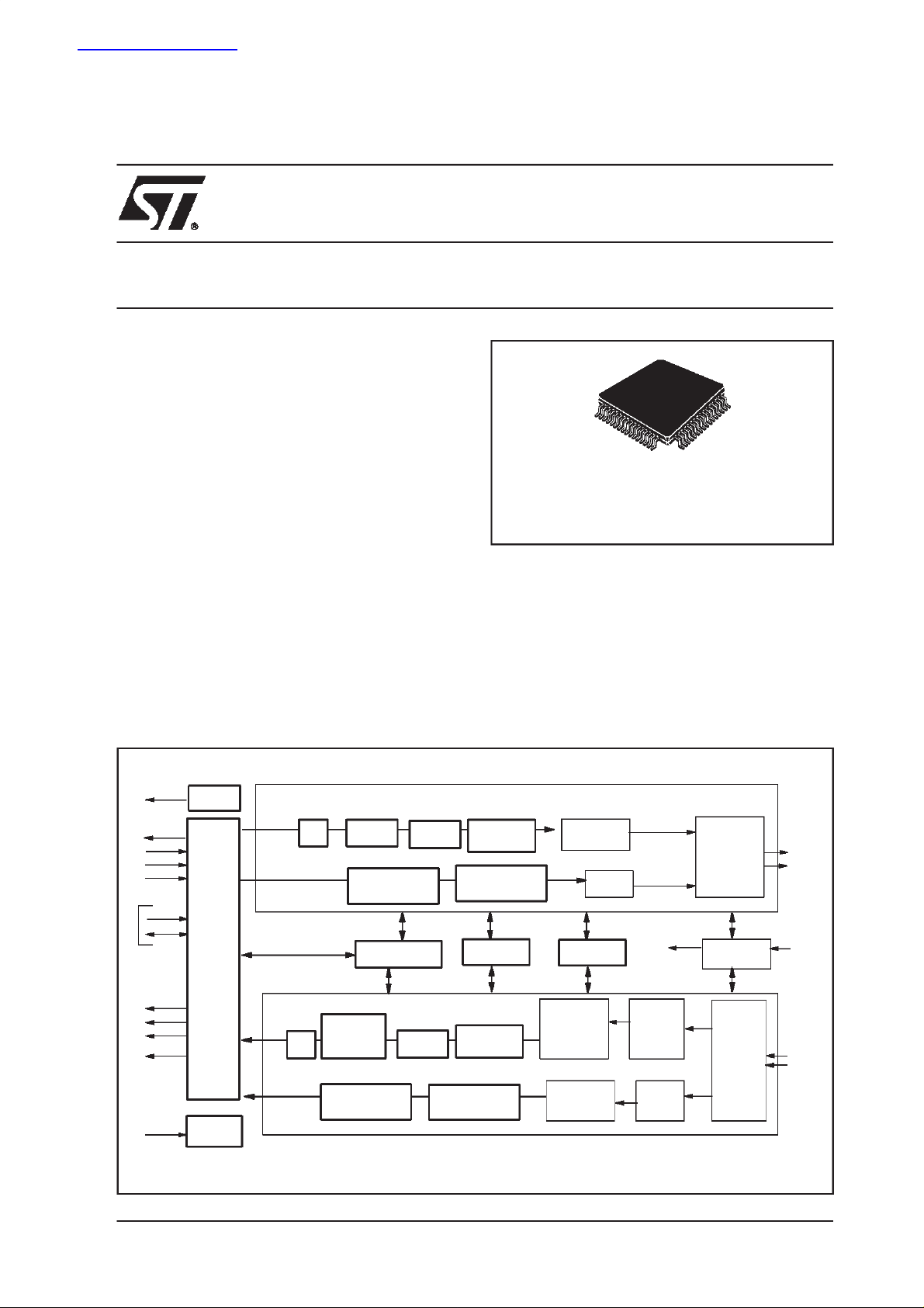
Figure 1. BLOCK DIAGRAM
LEDS
TX_CLK
TXD[3:0]
TX_ER
TX_EN
MDC
MDIO
Serial Management
RXD[3:0]
RX_ER
RX_DV
RX_CLK
HW
configuration
pins
LEDS
MII
Interface / Controller
HWConfig
PowerDown
100Mb/s
4B/5B
10Mb/s
100Mb/s
4B/5B
10Mb/s
Scrambler
NRZ ToManchester
Encoder
REGISTERS
Descrambler
CodeAlign
NRZ ToManchester
Encoder
TX Channel
Parallelto
Serial
RX Channel
Serial to
Parallel
NRZ ToNRZI
Encoder
Link Pulse
Generator
Auto
Negotiation
NRZI ToNRZ
Decoder
Link Pulse
Detector
Binary ToMLT3
Encoder
Loopback
Binary ToMLT3
Decoder
Clock Recovery
10 TX Filter
ClockRecovery
10 TX
Filter
Adaptive
Equalization
BaseLine
Wander
SMART
Squelch
TRANSMITTER
10/100
Clock
Generation
RECEIVER
10/100
TXP
TXN
System
Clock
RXP
RXN
January 2000
This ispreliminary information on a new product now in development. Details are subject to change without notice.
1/29
STE100P
2.2 Physical Layer
n Integrates the whole Physical layer functions of 100BASE-TX and 10BASE-T
n Provides Full-duplex operation on both 100Mbps and 10Mbps modes
n Provides Auto-negotiation(NWAY) function of full/half duplex operationfor both 10 and 100 Mbps
n Provides MLT-3 transceiver with DC restoration for Base-line wander compensation
n Provides transmit wave-shaper, receive filters, and adaptive equalizer
n Provides loop-back modes for diagnostic
n Builds in Stream Cipher Scrambler/ De-scrambler and 4B/5B encoder/decoder
n Supports external transmit transformer with turn ratio 1:1
n Supports external receive transformer with turn ratio 1:1
2.3 LED Display
n Provides 2 kinds of LED display mode:
•First mode - 3 LED displays for
♦ 100Mbps(on) or 10Mbps(off)
♦ Link(Keeps on when link ok) or Activity(Blink with10Hz whenreceiving or transmitting but not
collision)
♦ FD(Keeps on when in Full duplex mode) or Collision(Blink with 20Hz when colliding)
•Second mode – 4 LED displays for
♦ 100 Link(On when 100M link ok)
♦10 Link(On when 10M linkok)
♦ Activity (Blink with 10Hz when receiving or transmitting)
♦FD(Keeps on when in Full duplex mode) or Collision(Blink with 20Hz when colliding)
2.4 Miscellaneous
n Standard 64-pin QFP package pinout
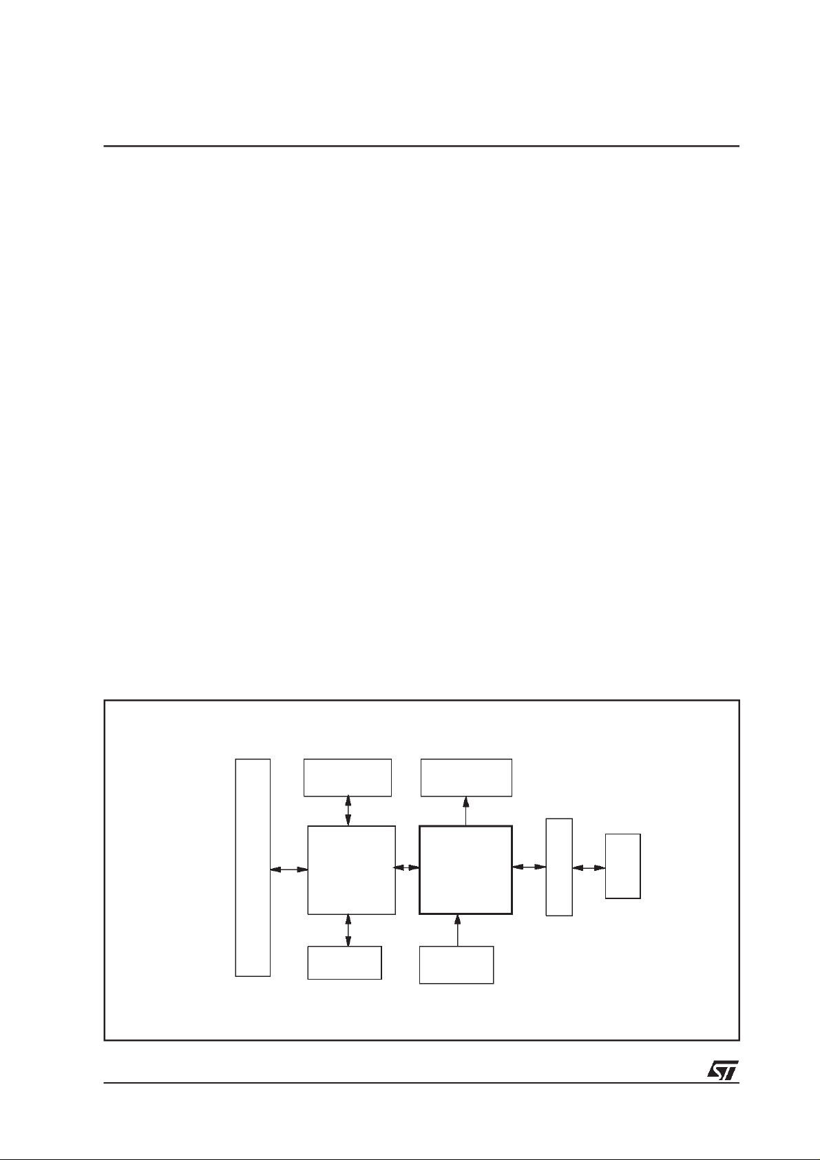
Figure 2. System Diagram of the STE100P Application
Serial
EEPROM
MAC
Device
PCI Interface
Boot ROM
STE100P
STEPHY1
25 MHz
Crystal
LEDs
RJ-45
Transformer
2/29
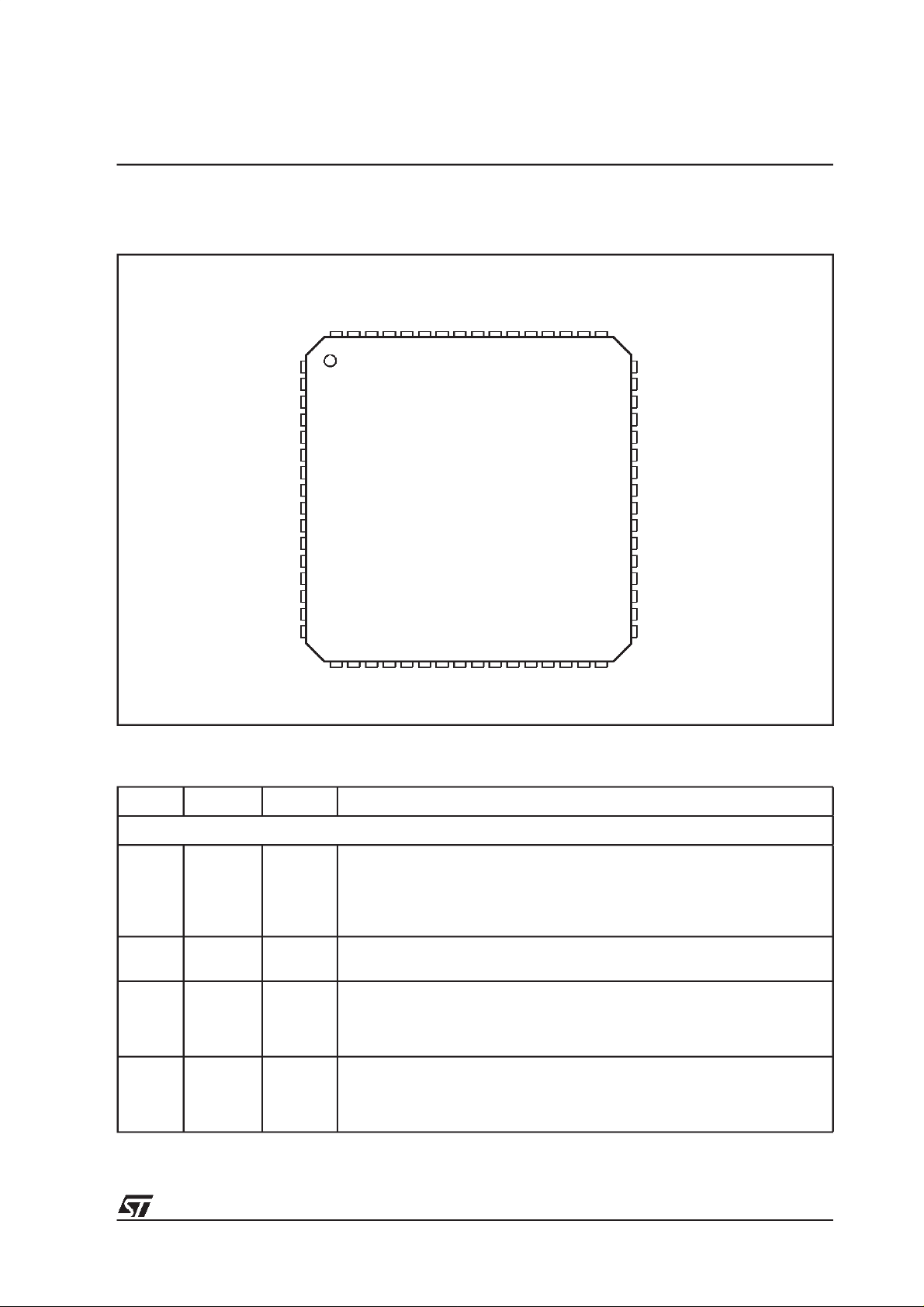
3.0 PIN ASSIGNMENT DIAGRAM
Figure 3. Pin Connection4.Pin Description
CRS
TDS/MDIR
VCCE/I
CFG1
CFG0VCCA
60
61
62
63
MF4
MF3
MF1
MF0
FDE
GNDE/I
GNDA
VCCA
GNDA
X2
X1
VCCA
GNDA
IREF
64
1
2
3
F2
4
5
6
7
8
9
10
12
13
14
15
16VCCA
17 18 19 20 21
59 58 57 56 5455 53 52 51 50 49
22 23 24 25 26
COL
TXD3
TXD2
TXD1
TXD0
TX_EN
TX_CLK
TX_ER/TXD
RX_ER/RXD
GNDE/I
271128 29 30 31 32
RX_CLK
48
47
46
45
44
43
42
41
40
39
38
37
36
35
34
33
STE100P
RX_DV
RXD0
RXD1
VCCE/I
RDX2
RDX3
MDC
MDIO
GNDE
VCCE
IEDR10
IEDTR
IEDL
IEDC
IEDS
SCAN_EN
RXN
RXP
GNDA
TXP
VCCA
TXN
GNDA
GNDE
TEST
RESET
VRDWN
RIP
N.C.
N.C.
N.C.
D99TL457
4.0 PIN DESCRIPTION
Table 1. Pin Description
Pin No. Name Type Description
MII Data Interface
59
58
57
56
55
TXD4
TXD3
TXD2
TXD1
TXD0
54 TX-EN I Transmit Enable. Thc MAC asserts this signal when it drives valid data on the
53 TX-CLK I/O Transmit Clock. Normally the STE100P drives TX-CLK. Refer to the Clock
52 TX-ER I Transmit Coding Error. The MAC asserts this input when an error has occurred
I Transmit Data. The Media Access Controller (MAC) drives data to the STE100P
using these inputs.
TXD4 is monitored only in Symbol (5B) Mode.
These signals must be synchronized to the TX-CLK.
TXD inputs. This signal mustbe synchronized to the TX-CLK.
Requirements discussion in the Functional Description section.
25 MHz for 100 Mbps operation.
2.5 MHz for 10 Mbps operation.
in the transmit data stream. Whenthe STE100P is operating at 100 Mbps, the
STE100P responds by sending invalid code symbols on the line. . In Symbol (5B)
Mode this pin is also equivalent to TXD4.
3/29

STE100P
Table 1. Pin Description
Pin No. Name Type Description
42
43
44
46
47
48 RX-DV O Receive Data Valid. ThcSTE100P asserts This signal when it drives valid data
51 RX-ER O Receive Error. The STE100P asserts this output when it receives invalid
49 RX-CLK O Receive Clock. This continuous clock provides reference for RXD. RXDV,and
60 COL O Collision Detected. The STE100P asserts this output when detecting acollision.
61 CRS O Carrier Sense. During half-duplex operation (PR0:8=0), the STE100P asserts
MII Control Interface
41 MDC I Management Data Clock. Clock for the MDIO serial data channel. Maximum
RXD4
RXD3
RXD2
RXD1
RXD0
O Receive Data. Thc STE100P drives received dataon these outputs,
synchronous to RX-CLK.
RXD4 is driven only in Symbol (5B) Mode.
on RXD. This output is synchronous to RX-CLK.
symbols from thenetwork. This signal is synchronous toRX-CLK. InSymbol (5B)
Mode this pin is also equivalent to RXD4.
RXER signals. Refer to the Clock Requirements discussion in the Functional
Description section.
25 MHz for 100 Mbps operation.
2.5 MHz for 10 Mbps operation.
This output remains High for the duration of the collision. This signal is
asynchronous and inactive during full-duplex operation.
this output when either transmit or receive medium is non idle. During full duplex
operation (PR0:8=1), CRS is asserted only when the receive medium is non-idle.
frequency is 2.5 MHz.
40 MDIO I/O Management DataInput/Output, Bi-directional serial data channel for PHY
communication.
62 MDINT OD Management DataInterrupt. When any bit in PR18= 1, an active Low output
on this pin indicates statuschange in the corresponding bits in PR17.
Interrupt is cleared by reading Register PR17
Physical (Twisted Pair) Interface
12 OSC1 I 25 MHz reference clock input. When an external 25MHz crystal is used, thispin
will be connected to one terminal of it. If an external 25 MHz clock source of
oscillator is used, then this pin will be theinput pin of it.
11 OSC2 O 25 MHz reference clock output. When an external 25MHz crystal is used, this pin
will be connected to another terminal of if. Ifan external clock source is used,
then this pin should be left open.
21
23
19
18
15 Iref O Reference Resistor connecting pin for reference current, directly connects a 5KΩ
TXP
TXN
RXP
RXN
O The differential Transmit outputs of 100BASE-TX or 10BASE-T, these pins
directly output to the transformer.
I The differential Receive inputs of 100BASE-TX or 10BASE-T,these pins directly
input from the transformer.
± 1% resistor to Vss.
4/29

Table 1. Pin Description
Pin No. Name Type Description
STE100P
37-33 LED/PAD
Pins
37 LED10/
PAD[4]
36 LEDTR/
PAD[3]
35 LEDL
/PAD[2]
34 LEDC
/
PAD[1]
I/O Pins 33-37 are multifunction pins used as LED outputs and PHY Address sensing
inputs for multiple PHY applications. PHY address sensing is achieved by
strapping a pull-up/pull-down resistor (typically 10 kΩ) to this pin as required.
The active state of each LED output driver is dependent on the logic level
sampled by the corresponding PHY address input upon power-up/reset. If a
given PAD input is resistively pulled low, the corresponding LED output will be
configured as an active high driver.Conversely, if a given PAD input is resistively
pulled high then the corresponding LEDoutput willbe configured as anactive low
driver.
These outputs are standard CMOS voltage drivers and not open-drain.
I/O LED display for 10Ms/s link status. This pin will be driven on continually when
10Mb/s network operating speed is detected.
The pull-up/pull-down status of this pin is latched into the PR20 bit 7 during
power up/reset.
LED display for Tx/Rx Activity status. This pin will be driven on with 10 Hz
blinking frequency when either effective receiving or transmitting is detected.
The status of thispin is latched into the PR20 bit 6 during power up/reset.
I/O LED display for Link Status. This pin will be driven on continually when a good
Link test is detected.
The status of thispin is latched into the PR20 bit 5 during power up/reset.
I/O LED display for Full Duplex or Collision status. This pin will be driven on
continually when a full duplex configuration is detected. This pin will be driven on
with 20 Hz blinking frequency when a collision status is detected in the half
duplex configuration.
The status of thispin is latched into the PR20 bit 4 during power up/reset.
33 LEDS
/
PAD[0]
31 CFG0 I Configuration Control 0.
32 CFG1 I Configuration Control 1.
Pin No. Name Type Description
29 RESET I Reset (Active-Low). This input must be held low for a minimum of 1 ms to reset
63 RIP O Reset In Progress. This output is used to indicate when the device has
I/O LED display for 100Ms/s link status. This pin will be driven on continually when
100Mb/s network operating speed is detected.
The status of thispin is latched into the PR20 bit 3 during power up/reset.
When A/N is enabled, CFG0 determines operating mode advertisement
capabilities in combination with CFG1 when MF0/ PR0:12 =1. (See Table2)
When A/N is disabled, CFG1 disables MLT3 and directly affects PR19:0
When CFG0 is Low,MLT3 encoder/decoder is enabled and PR19:1 =0.
When CFG0 is High, MLT3 encoder/decoder is bypassed and PR19:1 = 1.
When A/N is enabled, CFG1 determines operating mode advertisement
capabilities in combination with CFG1 when MF0/ PR0:12 =1. (See Table2)
When A/N is disabled, CFG1 enables Loopback mode and directly affects PR0
bit 14.
When CFG1 is Low,Loopback mode is disabled and PR0:14 = 0.
When CFG1 is High, Loopback mode is enabled and PR0:14 = 1.
the STE100P. During Power-up, the STE100P will be reset regardless of the
state of this pin, and this reset will not be complete until after >1ms.
completed power-up/reset and the registers and functions can be accessed.
When RIP is High, power-up/reset has been successful and the device can be
used normally
When RIP is Low, device reset is not complete.
5/29
STE100P
Table 1. Pin Description
Pin No. Name Type Description
30 PWRDWN I Power Down. WhenHigh, forces STE100P into Power Down mode. This pin is
5
4
3
2
1
6 FDE I Full-Duplex Enable.
MF0
MF1
MF2
MF3
MF4
OR’ed with the Power Down bit (PR0:11). During the Power Down mode, TXP/
TXN outputs and all LED outputs are 3-stated, and the MII interface isisolated.
I Multi-Function pins. Each MFpin internally drives different configuration
functions. The functions of the five MF inputs are as follows:
Pin Function Register & Bit Affected
MF0 Auto-Negotiation PR0:12 ANE
MF1 Enable NRZ-NRZI conversion PR19:7 ENRZI
MF2 4B/5B Coding Enable PR19:6 EN4B5B
MF3 Scrambler Operation Disable PR19:0 DISCRM
mf4 MF4 10/100 Mbps Speed Select PR0:13 SPSEL
The logic level of MF0-4 will determine the value that the affected bits will have
upon reset of the STE100P. The operating functions of CFG0, CFG1, and FDE
change depending on the state of MF0 (Auto-Negotiation enabled ordisabled).
Table 2 shows the relationship between CFG0, CFG1and FDE .
When A/N is enabled, FDE determines full-duplex advertisement capability in
combination with CFG0and CFG1. (SeeTable 2)
When A/N is disabled, FDE directly affects full-duplex operation and determines
the value of PR0 bit 8 (Full/Half Duplex Mode Select).
When FDE is High, full-duplex is enabled and PR0:8 = 1.
When FDE is Low, full-duplex is disabled and PR0:8 = 0.
Digital Power Pins
38, 45, 64 VCCE, VCCE/I
7, 25, 39, 50 GNDE, GNDE/I
Analog Power Pins
9, 13, 16, 17, 22 VCCA
8, 10, 14, 20, 24 GNDA
6/29

STE100P
5.0 HARDWARE CONTROL INTERFACE
5.1 Operating Configurations
TheHardware Control Interfaceconsistsof the MF<4:0>,CFG <1:0> andFDE input pinsas wellas theLED/
PADpins. This interfaceis used toconfigureoperatingcharacteristicsof theSTE100P. The Hardware Control
Interfaceprovides initialvalues for the MDIO registers,andthen passescontroltothe MDIO Interface. Individualchip addressing via the LED/PAD pins allowsmultipleSTE100P devicesto share the MII interface.Table 2
showshow to setup the desiredoperatingconfigurationsusing the Hardware ControlInterface.
Table 2. Operating Configurations / Auto-Negotiation Enabled
Desired
Configuration
Advertise All 1 1 1 1 1 1 1
Advertise 100 HD 1 0 0 0 1 0 0
Advertise 100 HD/FD 1 0 1 1 1 0 0
Advertise 10 HD 0 1 0 0 0 0 1
Advertise 10 HD/FD 0 1 1 0 0 1 1
CFG0 CFG1 FDE [8] TXF [7] TXH [6] 10F [5] 10H
Input Value PR4 Register Bits Affected
Advertise 10/100 HD 1 1 0 0 1 0 1
Note: If pin 5, MF0 = 0, or ANE (pinMF0 /PR0:12) = 0 (Auto-Negotiation disabled), then PR4 bits 5-8 will contain the default value indicated
in the table describing register PR4.
5.2 LED / PHY Address Interface
TheLED output pins can beusedto driveLED’s directly,or can be usedto providestatusinformationto a networkmanagementdevice. The activestate of each LED output driver is dependenton thelogic levelsampled
by the corresponding PHYaddress inputupon power-up/reset.For example, if a given PADinput isresistively
pulledlow thenthe corresponding LEDoutputwill be configured as an active highdriver. Conversely,if a given
PADinputis resistivelypulledhighthenthecorrespondingLEDoutputwill be configuredasan activelow driver.
These outputs are standard CMOS drivers and not open-drain.
The STE100P PAD[4:0]inputs provide up to 32 unique PHY address options. An address selection of all
zeros(00000) willresultin aPHY isolation condition asa result of power-on/reset
, asdocumented forPR0
bit11.
SeeSection 7 for more detaileddescriptions of deviceoperation.
6.0 REGISTERS AND DESCRIPTORS DESCRIPTION
Thereare 11 registerswith 16 bits each supportedforSTE100P. This includes7 basicregisterswhich are defined according to the clause 22 “Reconciliation Sub-layer and Media Independent Interface” and clause 28
“PhysicalLayer link signalingfor 10 Mb/s and 100Mb/s Auto-Negotiationon twisted pair” ofIEEE802.3ustandard.
Thereare 11 registerswith 16 bitseach supportedfor theSTE100P.Theseinclude 7 basicregisterswhichare
defined accordingto the clause 22 “ReconciliationSublayer and Media Independent Interface” and clause28
“PhysicalLayer link signalingfor 10 Mb/s and 100Mb/s Auto-Negotiationon twisted pair” ofIEEE802.3ustandard.
In addition, there are4 specialregistersfor advancedchip controland statusinformation.
7/29

STE100P
6.1 Register List
Table 3. Register List
Address Reg. Index Name Register Descriptions
0 PR0 XCR XCVR Control Register
1 PR1 XSR XCVR Status Register
2 PR2 PID1 PHY Identifier 1
3 PR3 PID2 PHY Identifier 2
4 PR4 ANA Auto-Negotiation Advertisement Register
5 PR5 ANLPA Auto-Negotiation Link Partner Ability Register
6 PR6 ANE Auto-Negotiation Expansion Register
17 PR17 XCIIS XCVR Configuration Information and InterruptStatus Register
18 PR18 XIE XCVR Interrupt Enable Register
19 PR19 100CTR 100BASE-TX PHY Control/Status Register
20 PR20 XMC XCVR Mode Control Register
6.2 Register Descriptions
Table 4. Register Descriptions
Bit # Name Descriptions Default Val RW Type
PR0- XCR, XCVR Control Register. The default values on power-up/resetare as listed below.
15 XRST Reset control.
1: Device will be reset. This bit will be cleared by STE100P
itself after the reset is completed.
14 XLBEN Loop-back mode select.
1: Loop-back mode is selected.
13 SPSEL Network Speed select. This bit’s selection will be ignored if
Auto-Negotiation is enabled(bit 12 of PR0 = 1).
1:100Mbps is selected.
0:10Mbps is selected.
12 ANEN Auto-Negotiation ability control.
1: Auto-Negotiation function is enabled.
0: Auto-Negotiation is disabled.
11 PDEN Power-down mode control.
1: Power-down mode is selected. Setting this bit puts the
STE100P into power-down mode. During the power-down
mode, TXP/TXNand all LED outputs are 3-stated, and the
MII interface is isolated.
0 R/W
0 R/W
1 R/W
1 R/W
0 R/W
8/29

Table 4. Register Descriptions
Bit # Name Descriptions Default Val RW Type
STE100P
10 ISOEN 0 – Normal operation.
1 – IsolatePHY from MII.
Setting this control bit isolates the STE100P from the MII,with
the exception of the serialmanagement inter-face. When this
bit is asserted, the STE100Pdoes not respond to TXD[3:0],
TX-EN, and TX-ER inputs, and it presents a high impedance
on its TX-CLK, RX-CLK, RX-DV, RX-ER, D[3:0], COL, and
CRS outputs. This bitis initialized to 0 unless the configuration
pins for the PHY address are set to 00000h during power-up
or reset.
9 RSAN Re-Start Auto-Negotiation process control.
1: Auto-Negotiation process will be re-started. This bit will be
cleared by STE100P itself afterthe Auto-negotiation
restarted.
8 DPSEL Full/Half duplex mode select.
1: full duplex mode is selected. This bit will be ignored if Auto-
Negotiation is enabled (bit 12 of PR0 = 1).
7 COLEN Collision test control.
1: collision test is enabled. 0: normal operation
This bit, when set, causes the COL signal to be asserted as a
result of the assertion of TX _EN within 512 BT.De-assertion
of TX_EN will cause the COL signal to be de-asserted within
4BT.
6~0 --- Reserved 0 RO
R/W = Read/Write able. RO = Read Only.
0 R/W
0 R/W
0 R/W
0 R/W
PR1- XSR, XCVR Status Register. All the bits of this register are read only.
15 T4 100BASE-T4 ability.
Always 0, since STE100P hasno T4ability.
14 TXFD 100BASE-TX full duplex ability.
0RO
1RO
Always1, sinceSTE100P has the100BASE-TX fullduplex ability.
13 TXHD 100BASE-TX half duplex ability.
Always1,since STE100Phas the 100BASE-TXhalfduplex ability.
12 10FD 10BASE-T full duplex ability.
Always 1, since STE100P has10Base-T full duplex ability.
11 10HD 10BASE-T half duplex ability.
Always 1, since STE100P has10Base-T half duplex ability.
10~7 --- Reserved 0 RO
6 MFPS MF Preamble Suppression
1 =Accepts management frames with pre-amble suppressed.
0 = Will not accept management frames with preamble
suppressed. Thevalue of thisbit iscontrolled by bit 1 of
PR20. Its default of 1 indicates that the SFEPHY1 accepts
management frame without preamble. A minimum of 32
preamble bits are required following power-on or hardware
reset. One IDLE bit is required between any two
management transactions as per IEEE 802.3u
specification.
1RO
1RO
1RO
1RO
9/29

STE100P
Table 4. Register Descriptions
Bit # Name Descriptions Default Val RW Type
5 ANC Auto-Negotiation Completed.
0: Auto-Negotiation process is not completed .
1: Auto-Negotiation process is completed.
4 RF Result of remote fault detection.
0: No remote fault condition detected.
1: Remote fault condition detected.
This bit is set when the Link Partner transmits a remote fault
condition (PR5 bit 13 = 1).
3 AN Auto-Negotiation ability.
Always 1, since STE100P hasthe Auto-Negotiation ability.
2 LINK Link status.
0: a failure link condition occurred. Read to set.
1: a valid link is established.
1 JAB Jabber detection.
1: jabber condition is detected (10Base-T only).
0 EXT Extended register supporting.
Always 1, since STE100P supports extended register
LL* = Latching Low and clear by read. LH* = Latching High and clear by read.
PR2- PID1,PHY Identifier 1
15~0 PHYID1 Part one of PHY Identifier.
Assigned to the 3rdto 18thbits of the Organizationally Unique
Identifier (OUI). (The ST OUI is 0080E1 hex).
0RO
0 RO/LH*
1RO
0 RO/LL*
0 RO/LH*
1RO
1C04h RO
PR3- PID2,PHY Identifier 2
15~10 PHYID2 Part two of PHY Identifier.
Assigned to the 19
Identifier (OUI).
9~4 MODEL Model number of STE100P.
Six bits manufacture’s model number.
3~0 REV Revision number of STE100P.
Four bits manufacture’s revision number.
PR4- ANA, Auto-Negotiation Advertisement
15 NXTPG Next Page ability.
Always 0: since STE100P does not provide next page ability.
14 --- Reserved
13 RF Remote Fault function.
1: with remote fault function.
12,11 --- Reserved
10 FC Flow Control function Ability.
1:supports PAUSE operation of flow control for full duplex link.
9 T4 100BASE-T4 Ability.
Always 0: since STE100P doesn’t have 100BASE-T4 ability.
th
000000b RO
to 24thbits ofthe Organizationally Unique
000001b RO
0001b RO
0RO
0 R/W
1 R/W
0RO
10/29

Table 4. Register Descriptions
Bit # Name Descriptions Default Val RW Type
STE100P
8 TXF 100BASE-TX Full duplex Ability.
1: with 100Base-TX full duplex ability.
7 TXH 100BASE-TX Half duplex Ability.
1: with 100Base-TX ability.
6 10F 10BASE-T Full duplex Ability.
1: with 10Base-T full duplex ability.
5 10H 10BASE-T Half duplex Ability.
1: with 10Base-T ability.
4~0 SF Select field. Default 00001=IEEE 802.3 00001 RO
PR5- ANLP,Auto-Negotiation Link Partner ability
15 LPNP Link partner Next Pageability.
0: link partner without next page ability.
1: link partner with next page ability.
14 LPACK Received Link Partner Acknowledge.
0: link code work had not received yet.
1 R/W
1 R/W
1 R/W
1 R/W
0RO
0RO
1:link partner successfully receivedSTE100P’sLink CodeWord.
13 LPRF Link Partner’s Remote fault status.
0: no remote fault detected.
1: remote fault detected.
12,11 --- Reserved 0 RO
10 LPFC Link Partner’s Flow control ability.
0: link partner without PAUSE function ability.
1: link partner with PAUSE function full duplex link ability.
0RO
0RO
9 LPT4 Link Partner’s 100BASE-T4 ability.
0: link partner without 100BASE-T4 ability.
1: link partner with 100BASE-T4 ability.
8 LPTXF Link Partner’s 100BASE-TX Full duplex ability.
0: link partner without 100BASE-TX full duplex ability.
1: link partner with 100BASE-TX full duplex ability.
7 LPTXH Link Partner’s 100BASE-TX Half duplex ability.
0: link partner without 100BASE-TX.
1: link partner with 100BASE-TX ability.
6 LP10F Link Partner’s 10BASE-T Full Duplex ability.
0: link partner without 10BASE-T full duplex ability.
1: link partner with 10BASE-T fullduplex ability.
5 LP10H Link Partner’s 10BASE-T Half Duplex ability.
0: link partner without 10BASE-T ability.
1: link partner with 10BASE-T ability.
4~0 LPSF Link partner select field. Default 00001=IEEE 802.3. 00001 RO
PR6- ANE, Auto-Negotiation expansion
15~5 --- Reserved 0 RO
0RO
0RO
0RO
0RO
0RO
11/29

STE100P
Table 4. Register Descriptions
Bit # Name Descriptions Default Val RW Type
4 PDF Parallel detection fault.
0: no fault detected.
1: a fault detected via parallel detection function.
3 LPNP Link Partner’s Next Page ability.
0: link partner without next page ability.
1: link partner with next page ability.
2 NP STE100P’s next Page ability.
Always 0, since STE100P without next page ability.
1 PR Page Received.
0: no new page has been received.
1: a new page has been received.
0 LPAN Link Partner Auto-Negotiation ability.
0: link partner has no Auto-Negotiation ability.
1: link partner has Auto-Negotiation ability.
LH = High Latching and cleared by reading.
PR17- XCIIS, XCVR Configuration information and Interrupt Status
0 RO/LH*
0RO
0RO
0 RO/LH*
0RO
15~10 ---- Reserved 0 RO
9 SPEED Configured information ofSpeed.
0: the speed is 10Mb/s.
1: the speed is 100Mb/s.
8 DUPLEX Configured information of Duplex.
0: the duplex mode is half.
1: the duplex mode is full.
0RO
0RO
7 PAUSE Configured information of PAUSE function for flow control.
0: PAUSEfunction is disabled.
1: PAUSEfunction is enabled
6 ANC Interrupt source of Auto-Negotiation Completed.
0: Auto-Negotiation has not completed yet.
1: Auto-Negotiation has completed.
5 RFD Interrupt source of Remote Fault Detected.
0: there is no remote fault detected.
1: remote fault is detected.
4 LS Interrupt source of Link Fail.
0: link test status is up.
1: link is down.
3 ANAR Interrupt source of Auto-Negotiation Acknowledge Received.
0: there is no link code word received.
1: link code word is receive from link partner.
2 PDF Interrupt source of Parallel Detection Fault.
0: there is no parallel detection fault.
1: parallel detection is fault.
1 ANPR Interrupt source of Auto-Negotiation Page Received.
0: there is no Auto-Negotiation page received.
1: auto-negotiation page is received.
0RO
0 RO/LH*
0 RO/LH*
0 RO/LH*
0 RO/LH*
0 RO/LH*
0 RO/LH*
12/29

Table 4. Register Descriptions
Bit # Name Descriptions Default Val RW Type
STE100P
0 REF Interrupt source of Receive Error full.
0: the receive error number is less than 64.
1: 64 error packets are received.
LH = High Latching and cleared by reading.
PR18- XIE, XCVR Interrupt Enable Register
15~7 --- Reserved
6 ANCE Auto-Negotiation Completed interrupt Enable.
0: disable Auto-Negotiation completed interrupt.
1: enable Auto-Negotiation complete interrupt.
5 RFE Remote Fault detected interrupt Enable.
0: disable remote fault detection interrupt.
1: enable remote fault detection interrupt.
4 LDE Link Down interrupt Enable.
0: disable link failinterrupt.
1: enable link failinterrupt.
3 ANAE Auto-Negotiation Acknowledge interrupt Enable.
0: disable link partner acknowledge interrupt
1: enable link partner acknowledge interrupt.
2 PDFE Parallel Detection Fault interrupt Enable.
0: disable fault parallel detection interrupt.
1: enable fault parallel detection interrupt.
1 ANPE Auto-Negotiation Page Received interrupt Enable.
0: disable Auto-Negotiation page received interrupt.
1: enable Auto-Negotiation page received interrupt.
0 RO/LH*
0 R/W
0 R/W
0 R/W
0 R/W
0 R/W
0 R/W
0 REFE RX_ERR full interrupt Enable.
0: disable rx_err fullinterrupt.
1: enable more than64 time rx_err interrupt,
PR19- 100CTR, 100BASE-TX Control Register
15,14 --- reserved
13 DISRER Disable the RX_ERR counter.
0: the receive error counter - RX_ERR is enabled.
1: the receive error counter - RX_ERR is disabled.
12 ANC Auto-Negotiation completed. This bit is the sameas PR1:5.
0: the Auto-Negotiation process has not completed yet.
1: the Auto-Negotiation process has completed.
11 RXVPP Select peak to peak voltage of receive.
0: receive voltage peak to peak 1.0 VPP
1: receive voltage peak to peak 1.4 VPP.
10 --- reserved
9 ENRLB Enable remote loop-back function. 1: enable 0: disable 0 R/W
8 ENDCR Enable DC restoration.
0: disable DC restoration.
1: enable DC restoration.
0 R/W
0 R/W
0RO
0 R/W
1 R/W
13/29

STE100P
Table 4. Register Descriptions
Bit # Name Descriptions Default Val RW Type
7 ENRZI Enable the conversions between NRZ and NRZI.
0: disable the data conversion between NRZ and NRZI.
1: enable the data conversion of NRZI to NRZ in receiving and
NRZ to NRZI in transmitting.
6 EN4B5B Enable 4B/5B encoder and decoder
0: the 4B/5B encoder and decoder are bypassed
1: the 4B/5B encoder and decoder are enabled..
5 ISOTX Transmit Isolation. When 1, isolate from MII and tx+/-. The bit
will be setto one if thePHY address is set to 00000 at power-
up/reset This bit must be 0for normal operation
4~2 CMODE Reporting of current operation mode of transceiver.
000: in auto-negotiation
001: 10Base-T half duplex
010: 100Base-TX half duplex
011: reserved
100: reserved
101: 10Base-T full duplex
110: 100Base-TX full duplex
111: isolation, auto-negotiation disable
1 DISMLT Disable MLT3.
0: the MLT3 encoder and decoder are enabled.
1: the MLT3 encoder and decoder are bypassed.
0 DISCRM Disable Scramble.
0: the scrambler and de-scrambler is enabled.
1: the scrambler and de-scrambler are disabled.
1 R/W
1 R/W
0 R/W
000 RO
0 R/W
0 R/W
PR20- XMC, XCVR Modecontrol
15~12 --- Reserved 0 RO
11 LD Long Distance mode of 10BASE-T.
0: normal squelch level.
1: reduces 10Base-T squelch level for extended cable length.
As the length of the cable increases, so does the current.
10~8 --- Reserved 0 RO
7~3 PAD4:0 PHY Address [4:0]:
The values of the PAD[4:0] pins are latched to this register at
power-up/reset. The first PHY address bit transmitted or
received is the MSB of the address (bit 4). A station
management entity connected to multiple PHY entities must
know the appropriate address of each PHY.A PHY address of
<00000> that is latched into the part at power-up/reset will
cause the Isolate bitof thePR0 (bit 10, register address 00h)
to be set.
After power up/reset the only way to enable or disable isolate
mode is to set or clear the Isolate bit (bit 10) PR0. After power
up/reset writing <00000> to bits [4:0] of this register will not
cause the part toenter isolate mode.
2 --- reserved 0 RO
0 R/W
[00001] Strap,
R/W
14/29

Table 4. Register Descriptions
Bit # Name Descriptions Default Val RW Type
STE100P
1 MFPSE MF Preamble Suppression Enable
1 = Accept management frames with pre-amble suppressed.
0 = Do not accept management frames with preamble
suppressed.
This bit also controls the value of bit 6 in PR1 (MFPS).
0 --- reserved 0 RO
1 R/W
7.0 DEVICE OPERATION
TheSTE100PintegratestheIEEE802.3ucompliantfunctionsof PCS(physicalcodingsub-layer), PMA(physical
medium attachment) sub-layer, and PMD(physical medium dependent) sub-layer for 100BASE-TX, and the
IEEE802.3compliantfunctionsof Manchesterencoding/decoding and transceiver for 10BASE-T.All thefunctionsand operationschemes are describedin the followingsections.
7.1 100BASE-TX Transmit Operation
Regarding the 100BASE-TX transmission,the device provides the transmission functionsof PCS, PMA,and
PMD for encoding of MII data nibbles to five-bit code-groups (4B/5B), scrambling, serializationof scrambled
code-groups, convertingthe serial NRZ codeinto NRZI code, converting the NRZI code into MLT3 code,and
thendrivingthe MLT3 code into the category5 UnshieldedTwistedPair cablethroughan isolation transformer
withthe turnsratio of 1.414: 1.
Data code-groups Encoder: InnormalMII modeapplication, the device receivesnibbletype4B datavia
the TxD0~3 inputs of theMII. These inputs are sampled by the device on the rising edge of Tx-clk and
passedtothe 4B/5B encoderto generatethe 5B code-groupused by 100BASE-TX.
Idle code-groups:In ordertoestablishand maintain theclocksynchronization, the device needs to keep
transmittingsignalsto the medium.The devicewillgenerateIdle code-groups fortransmissionwhenthere
is noreal datawantto be sentby MAC.
Start-of-Stream Delimiter-SSD (/J/K/): In a transmissionstream,the first16 nibbles are MAC preamble.
In orderto let partnerdelineate the boundaryof a data transmissionsequence and to authenticatecarrier
events,thedevicewillreplacethe first2 nibblesof the MAC preamblewith /J/K/code-groups.
End-of-Stream Delimiter-ESD (/T/R/): In order to indicate the terminationof the normal data transmis-
sions,the device will insert2 nibbles of /T/R/code-group after thelastnibbleof FCS.
Scrambling: All the encodeddata(includingthe idle,SSD, and ESD code-groups) is passed to thedata
scrambler to reduce the EMI andspread the powerspectrumusing a 10-bitscramblerseed loadedat the
beginning.
Data conversion of Parallel to Serial, NRZ to NRZI, NRZI to MLT3: Afterscrambled,the transmission
data with 5B typein 25MHz will be converted to serialbit streamin 125MHzby the parallel toserialfunction. Afterserialized,thetransmissionserialbitstreamwill be furtherconvertedfrom NRZto NRZIformat.
This NRZI conversionfunction can be bypassed,if the bit 7 of PR19 register is clearedas 0. AfterNRZI
converted,the NRZIbit streamis passedthrough MLT3encoderto generatethe TP-PMDspecifiedMLT3
code. Withthis MLT3 code,it lowersthe frequency and reduces the energyof the transmissionsignalin
theUTP cableandalso makes the systemeasily to meet theFCC specificationof EMI.
Wave-Shaper and Media Signal Driver: In ordertoreducethe energy ofthe harmonicfrequencyoftrans-
missionsignals,the device providesthe wave-shaper priortotheline driver to smooth but keep symmetric
the rising/falling edge of transmissionsignals. The wave-shaped signals include the 100BASE-TX and
10BASE-T both are passedto the same mediasignal driver. This designcan simplifythe external magneticconnection withsingleone.
15/29

STE100P
7.2 100BASE-TX Receiving Operation
Regardingthe100BASE-TX receivingoperation,the deviceprovidesthereceiving functionsofPMD, PMA,and
PCSfor receivingincomingdata signalsthrough category5 UTPcableand an isolation transformer with turns
ratioof 1: 1. It includesthe adaptiveequalizer and baselinewander, data conversions of MLT3to NRZI,NRZI
to NRZand serial to parallel,thePLL for clock and data recovery,the de-scrambler,and thedecoderof 5B/4B.
Adaptive Equalizer and Baseline Wander: Since thehighspeedsignalsover the unshielded(or shield-
ed)twistedPair cablewill inducetheamplitudeattenuationand phaseshifting. Furthermore,theseeffects
aredepends onthe signal frequency,cable type, cable length and the connectorsof the cabling.So a reliableadaptiveequalizerandbaselinewandertocompensateallthe amplitudeattenuationandphaseshiftingare necessary. In thetransceiver,it providesthe robust circuitsto performthese functions.
MLT3 toNRZI Decoder and PLL for Data Recovery: Afterreceivingtheproper MLT3signals,thedevice
convertsthe MLT3 to NRZI code for further processing. After adaptive equalizer, baseline wander, and
MLT3toNRZIdecoder, thecompensatedsignals withNRZItypein125MHzare passedtothe PhaseLock
Loopcircuitsto extractout the original data and synchronous clock.
Data Conversions of NRZI to NRZ and Serial to Parallel: After data is recovered, the signalswill be
passedtotheNRZIto NRZ converterto generatethe 125 MHzserialbit stream.This serialbit streamwill
bepackedto parallel5B typefor furtherprocessing. TheNRZI to NRZ conversioncan be bypassed,if the
bit 7 of PR19 registeris clearedas 0.
De-scrambling andDecoding of 5B/4B: The parallel5B type data is passed to de-scramblerand5B/4B
decoder to returntheir originalMII nibble type data.
Carrier sensing:CarrierSense(CRS)signalisassertedwhenthe STE100Pdetectsany 2 non-contiguous
zeroswithin any 10 bit boundary of the receivingbit stream.CRS is de-assertedwhenESD code-group or
Idlecode-groupis detected. Inhalf duplex mode,CRS is assertedduringpacket transmissionorreceive.
But in full duplex mode, CRS is assertedonly during packet reception.
7.3 10BASE-T Transmission Operation
This includesthe parallel to serial converter,Manchester Encoder, Link test function, Jabber function and the
transmit wave-shaper and line driver described in the section of “Wave-Shaper and Media Signal Driver” of
“100BASE-T TransmissionOperation”. It also provides Collisiondetectionand SQE testfor halfduplex application.
7.4 10BASE-T Receive Operation
Thisincludesthecarriersensefunction,receivingfilter,PLLforclockanddatarecovering,Manchesterdecoder,
andserialto parallelconverter.
7.5 Loop-back Operation
TheSTE100Pprovides internal loop-backoption forboththe 100BASE-TX and10BASE-T operations. Setting
bit14 of PR0 register to 1 canenable the loop-backoption. In thisloop-back operation, the TX±and RX±lines
areisolatedfrom the media. TheSTE100P also providesremote loop-back operationfor 100BASE-TXoperation.Settingbit 9 of PR19registerto 1 enablesthe remote loop-back operation.
In the 100BASE-TX internalloop-back operation,the data comes fromthe transmitoutputof NRZtoNRZIconverterthen loop-back tothe receive path into the input of NRZI to NRZ converter.
Inthe100BASE-TX remoteloop-back operation, thedata is receivedfromRX± pinsthroughreceivepath tothe
output of data and clock recover and then loop-back to the input of NRZI to MLT3 converter of transmit path
thentransmit out to the mediumvia thetransmit line drivers.
In the 10BASE-T loop-back operation, the data is through transmit path and loop-back from the outputof the
Manchesterencoderintothe input of PhaseLock Loop circuitof receive path.
16/29

STE100P
7.6 Full Duplex and Half Duplex Operation
TheSTE100Pcanoperate for either full duplex or half duplexnetwork application.In full duplex, both transmit
andreceivecan be operatedsimultaneously.Under full duplex mode,collision(COL) signalis ignoredand carriersense(CRS)signalis assertedonlywhen the STE100Pis receiving.
In half duplex mode, either transmitor receive can be operatedat one time. Under half duplex mode, collision
signal is assertedwhen transmit and receivesignals collidedand carrier sense assertedduring transmission
andreception.
7.7 Auto-Negotiation Operation
TheAuto-Negotiationfunctionis designedto providethe meanstoexchangeinformationbetweentheSTE100P
andthenetworkpartnerto automaticallyconfigure both to takemaximumadvantageof theirabilities,and both
aresetup accordingly.The Auto-Negotiation functioncan be controlledthrough ANE,bit12 of the PR0register,
or the MF0 pin5.
Auto-Negotiationexchanges informationwith the network partner using the FastLink Pulses(FLPs)- a burstof
linkpulses. Thereare16 bits ofsignaling informationcontained in the burst pulses to advertiseall remotepartner’scapabilitieswhich aredeterminedby theregisterof PR4.Accordingto this informationthey find outtheir
highestcommon capabilityby followingthe priority sequence as below:
1. 100BASE-TXfull duplex
2. 100BASE-TXhalf duplex
3. 10BASE-T full duplex
4. 10BASE-T half duplex
During power-up or reset,if Auto-Negotiationis foundenabledthenFLPswill be transmitted and theAuto-Negotiationfunctionwill procede. Otherwise,the Auto-Negotiationwill not occuruntil the bit 12 ofPR0 register is
setto 1. When Auto-Negotiation is disabled, then the NetworkSpeed and Duplex Mode are selectedby programmingPR0register.
7.8 Power Down Operation
To reduce the power consumption, the STE100Pis designed with a power downfeature, which can save the power
consumption significantly. Since the power supply of the 100BASE-TX and 10BASE-T circuits are separated, the
STE100P can turn off the circuit of either the 100BASE-TX or 10BASE-T when the other one of them is operating.
Thereis alsoa Power Downmode which can be selectedby PDEN in register PR0 bit 11. During the Power Down
mode, TXP/TXNoutputs and all LEDoutputsare 3-stated,and the MIIinterfaceis isolated.DuringPowerDown mode
the MIImanagement interfaceis still available for readingand writing device registers. PowerDownmode canbe exited by clearing bit 11 of registerPR0 or by a hardware or software reset (settingPR0:15=1).
7.9 LED Display Operation
TheSTE100Pprovides 2 functionsfor the LEDpins, thedetail descriptionsabout the operation are described
in the PIN Descriptionsection, and asfollows.
•Firstmode- 3 LED displaysfor:
•100Mbps (on) or 10Mbps(off)
•Link (Stayson whenlinkokay) orActivity (Blinksat 10Hz when receivingor transmitting,but notcollision)
•FD (Stayson whenin Fullduplex mode) or Collision(Blinks at 20Hz when a collisionoccurs)
•Secondmode – 4 LED displaysfor:
•100 Link (On when 100M link is okay)
•10 Link (Onwhen 10M link is okay)
•Activity(Blinks at 10Hzwhen receivingor transmitting)
•FD (Stayson whenin Fullduplex mode)or Collision(Blinks at 20Hzwhen a collisionoccurs)
17/29

STE100P
7.10Reset Operation
Thereare twowaysto resettheSTE100P. First, for hardware reset, the STE100P can be resetvia RESETpin
(pin29). Theactivelow Resetinput signalis required at least1 ms toensure properresetoperation. Second,
for softwarereset,whenbit 15 of registerPR0is setto 1,the STE100Pwill reset entirecircuitsand registersto
their default values,then clearthe bit 15 of PR0to 0, and set the RIP outputpin 63 to logic 1. Both hardware
andsoftwarereset operations initialize all registersto theirdefaultvalues.This process includesre-evaluation
of all hardware-configurableregisters. Logiclevels on severalI/O pins are detectedduringhardware reset periodto determinethe initial functionality of STE100P. Some of these pins are used as outputsafter the reset
operation. Care must be taken to ensure that the configuration setup will not interfere with normal operation.
Dedicatedconfiguration pins can be tiedto theVcc or ground directly.Configurationpins multiplexedwith LED
outputs shouldbe weaklypulled up or weaklypulleddownthroughresistorsas shown in the following circuits.
I/OPIN
I/OPIN
10kΩ
Logic Level 1
Vcc
10kΩ
Logic Level 0
7.11Preamble Suppression
Preamblesuppression modein the STEPHY1 is indicatedby a one inbit six of the PR1Register. If it is determined that allPHY devicesin the systemsupportpreamblesuppression, then a preamble is not necessaryfor
eachmanagementtransaction. The first transactionfollowingpower-up/hardwareresetrequires32 bits of preamble. Thefull 32 bit preamble is not required for eachadditional transaction. TheSTEPHY1will respondto
management accesseswithout preamble,but a minimumof one idle bit between managementtransactions is
required as specified in IEEE 802.3u.
7.12Remote Fault
Theremotefaultfunctionindicatestoalinkpartnerthatafaultconditionhas occurredbyusingtheRemoteFault
bit,whichis encodedin bit 13 of the LinkCodeWord. A local deviceindicatesto its linkpartnerthatit hasfound
a fault by setting the Remote Fault bit inthe Auto-Negotiationregister to logic one and renegotiating with the
link partner. The Remote Faultbit remains at logicone until successful negotiation with the Link Code Word
occurs. The bit will then returnto 0. Whenthe messageis sent thattheRemoteFault bit is set to logic one, the
devicewill setthe RemoteFault bit in the MII to logicone if the managementfunctionis present.
7.13Transmit Isolation
RxD
18/29
TxD
STA/STE
4/5
4/5
MII
STEPHY1
TX(100MHz)/TP(10MHz)
Ethernet
ttp
tpn

STE100P
8.0 ELECTRICAL SPECIFICATIONS AND TIMINGS
Table 5. Absolute Maximum Ratings
Parameter Value
Supply Voltage(Vcc) -0.5 V to 7.0 V
Input Voltage -0.5 V to VCC + 0.5 V
Output Voltage -0.5 V to VCC + 0.5 V
Storage Temperature -65 °C to 150 °C(-85°F to 302°F)
Ambient Temperature 0°Cto70°C(32°F to 158°F)
ESD Protection 2000V
Table 6. GeneralDC Specifications
Symbol Parameter Test Condition Min. Typ. Max. Units
General DC
Vcc Supply Voltage 3.15 3.3 3.45 V
Icc Power Supply 100 mA
10BASE-T Voltage/Current Characteristics
Rid10 Input Differential Resistance DC TBD kΩ
Vida10 Input Differential Accept Peak
Voltage
Vidr10 Input Differential Reject Peak
Voltage
Vicm10 Input Common Mode Voltage TBD V
Vod10 Output Differential Peak Voltage 2200 2800 V
Icct10 Line Driver Supply TBD mA
100BASE-TX Voltage/CurrentCharacteristics
Rid100 Input Differential Resistance TBD kΩ
Vida100 Input Differential Accept Peak
Voltage
Vidr100 Input Differential Reject Peak
Voltage
Vicm100 Input Common Mode Voltage TBD V
Vod100 Output Differential Peak Voltage 950 1050 V
5MHz ~ 10MHz 585 3100 mV
5MHz ~ 10MHz 0 585 mV
200 1000 mV
0 200 mV
Icct100 Line Driver Supply TBD mA
19/29

STE100P
Table 7. AC Specifications
Symbol Parameter Test Condition Min. Typ. Max. Units
X1 Specifications
TX1d X1 Duty Cycle 45 50 55 %
TX1p X1 Period 30 ns
TX1t X1 Tolerance PPM
10BASE-T Normal Link Pulse(NLP) Timings Specifications
TNPW NLP Width 10Mbps 100 ns
TNPC NLP Period 10Mbps 8 24 ms
Figure 4. Normal Link Pulse timings
Tnpw
Tnpc
Table 7. AC Specifications
Symbol Parameter Test Condition Min. Typ. Max. Units
Auto-Negotiation Fast Link Pulse(FLP) Timings Specifications
Tflpw FLP Width 100 ns
Tflcpp Clock pulse to clock pulse period 111 125 139 µs
Tflcpd Clock pulse to Data pulse period 55.5 62.5 69.5 µs
- Number of pulses in one burst 17 33 pulse
Tflbw Burst Width 2ms
Tflbp FLP Burst period 8 16 24 ms
20/29

Figure 5. Fast Link Pulse timing
STE100P
Tflcpp
Tflcpd
Tflpw
Tflbw
Tflbp
Table 7. AC Specifications
Symbol Parameter Test Condition Min. Typ. Max. Units
100BASE-TX Transmitter AC TimingsSpecification
Tjit TDP-TDN Differential Output
MII Management Clock Timing Specifications
Peak Jitter
t1 MDC Low PulseWidth 200 — ns
t2 MDC High Pulse Width 200 — ns
t3 MDC Period 400 — ns
t4 MDIO(I) Setup to MDC Rising
Edge
10 — ns
1.4 ps
t5 MDIO(O) Hold Time from MDC
Rising Edge
t6 MDIO(O) Valid from MDC Rising
Edge
10 — ns
0 300 ns
21/29

STE100P
Figure 6. MII Management Clock Timing
t1
t2
t3
MDC
t4 t5
MDIO(I)
t6
MDIO(O)
Table 7. AC Specifications
Symbol Parameter Test Condition Min. Typ. Max. Units
MII Receive Timing Specification
t1 RX-ER, RX-DV,RXD[3:0] Setup
to RX-CLK
t2 RX-ER, RX-DV,RXD[3:0] Hold
After RX-CLK
10 — ns
10 — ns
t3 RX-CLK High Pulse Width(100
Mbits/s)
RX-CLK High Pulse Width(10
Mbits/s)
t4 RX-CLK Low Pulse Width (100
Mbits/s)
RX-CLK Low Pulse Width (10
Mbits/s)
t5 RX-CLK Period (100 Mbits/s) 40 ns
RX-CLK Period (10 Mbits/s) 400 ns
14 26 ns
200 ns
14 26 ns
140 260 ns
22/29

STE100P
Figure 7. MII Receive Timing
Table 7. AC Specifications
Symbol Parameter Test Condition Min. Typ. Max. Units
MII Transmit Timing Specification
t1 TX-ER,TX-EN,TXD[3:0] Setup to
TX-CLK Rise
t2 TX-ER,TX-EN,TXD[3:0] Hold
After TX-CLK Rise
Figure 8. MII TransmitTiming
10 — ns
025ns
23/29

STE100P
Table 7. AC Specifications
Symbol Parameter Test Condition Min. Typ. Max. Units
Receive Timing Specification
Rt1 Receive Frame to Sampled Edge
of RX-DV
(100 Mbits/s)
Receive Frame to Sampled Edge
of RX-DV
(10 Mbits/s)
Rt2 Receive Frame to CRS High
(100Mbits/s)
Receive Frame to CRS High (10
Mbits/s)
Rt3 End of Receive Frame to
Sampled Edge of RX-DV (100
Mbits/s)
End Receive Frame to Sampled
Edge of RX-DV (10 Mbits/s)
Rt4 End of Receive Frame to CRS
Low (100 Mbits/s)
End of Receive Frame to CRS
Low (10 Mbits/s)
Figure 9. Receive Timing
— 15 bits
— 22 bits
—13Bits
— 5 bits
— 12 bits
— 4 bits
13 24 bits
— 4.5 bits
24/29

STE100P
Table 7. AC Specifications
Symbol Parameter Test Condition Min. Typ. Max. Units
Transmit TimingSpecification
t1 TX-EN Sampled to CRS High
(100 Mbits/s)
TX-EN Sampled to CRS High (10
Mbits/s)
t2 TX-EN Sampled to CRS Low
(100 Mbits/s)
TX-EN Sampled toCRS Low (10
Mbits/s)
t3 Transmit Latency (100 Mbits/s) 6 14 bits
Transmit Latency (10 Mbits/s) 4 — bits
t4 Sampled TX-EN Inactive to End
of Frame
(100 Mbits/s)
Sampled TX-EN Inactive to End
of Frame
(10 Mbits/s)
0 4 bits
— 1.5 bits
0 16 bits
— 16 bits
— 17 bits
— 5 bits
Figure 10. Transmit Timing
25/29

STE100P
Figure: 11 Transmit Timing
TXP
Parameter Sym Min Typ Max Units
TXD, TX_EN, TX_ER Setup to TX_CLK High t2A 10 - - ns
TXD, TX_EN, TX_ER Hold from TX_CLK High t2B 5 - - ns
TX_EN sampled to CRS asserted t2C - 3 4 BT
TX_EN sampled to CRS de-asserted t2D - 4 16 BT
TX_EN sampled to TXP out(Tx latency) t2E 6 10 14 BT
BT is the duration of one bitas transferred to and from the MAC and is the reciprocal of the bit rate.
26/29

Figure 12: 10Base-T Transmit Timing
TXP
STE100P
Parameter Sym Min Typ Max Units
TXD, TX_EN, TX_ER Setup to TX_CLK High t8A 10 - - ns
TXD, TX_EN, TX_ER Hold from TX_CLK High t8B 5 - - ns
TX_EN sampled to CRS asserted t8C - 0 4 BT
TX_EN sampled to CRS de-asserted t8D - 8 BT
TX_EN sampled to TXP out(Tx latency) t8E - 3-5 BT
BT is the duration of one bitas transferred to and from the MAC and is the reciprocal of the bit rate.
27/29

STE100P
28/29

STE100P
PACKAGE TYPE: TQFP 64L/ BODY 10X10X1.40mm / FOOT PRINT 1.00 mm
DIMENSIONS
DATABOOK mm DRAWINGmm DRAWING inch
REF
TYP MIN MAX TYP MIN MAX TYP MIN MAX
A
A1
A2
B
c
D
D1
D3
e
E
E1
E3
L
L1
K
1.60 1.420 1.540 .056 .061
0.05 0.15 0.100 0.065 0.135 .004 .003 .005
1.40 1.35 1.45 1.400 1.360 1.440 .055 .054 .057
0.22 0.17 0.27 0.200 0.175 0.225 .008 .007 .009
0.09 0.20 0.165 .006
12.00 12.00 11.90 12.10 .472 .469 .476
10.00 10.00 9.975 10.025 .394 .393 .395
7.50 7.500 7.450 7.550 .295 .293 .297
0.50 0.500 0.450 0.550 .020 .018 .022
12.00 12.00 11.90 12.10 .472 .469 .476
10.00 10.00 9.975 10.025 .394 .393 .395
7.50 7.500 7.450 7.550 .295 .293 .297
0.60 0.45 0.75 0.450 .018
1.00 1.000 0.938 1.063 .039 .037 .042
3.5d 0d 7d 3.5d 1.5d 5.5d 3.5d 1.5d 5.5d
Information furnished is believed to be accurate and reliable. However, STMicroelectronics assumes no responsibility for the consequences
of use of such information nor for any infringement of patents or other rights of third parties which mayresult from its use. Nolicense is granted
by implicationor otherwise under any patent or patent rights of STMicroelectronics. Specifications mentioned in this publication are subject
to change without notice. This publication supersedes and replaces all information previously supplied. STMicroelectronics products are not
authorized for use as critical components in lifesupport devices or systems without express writtenapproval of STMicroelectronics.
The ST logo is a registered trademark of STMicroelectronics
1999 STMicroelectronics - All Rights Reserved
Australia - Brazil - China - Finland - France - Germany - Hong Kong - India - Italy - Japan - Malaysia - Malta - Morocco - Singapore - Spain
29/29
STMicroelectronics GROUP OFCOMPANIES
- Sweden - Switzerland - United Kingdom - U.S.A.
http://www.st.com
 Loading...