

Page 1
STDP3100
DisplayPort to VGA converter
Data Brief
Features
■ Two lane DisplayPort™ 1.1a receiver
■ Triple 10-bit video DAC
– 162 MSPS throughput rate
– VSIS compatible
– RGB output with 0 to 700mV range
■ 3.3V HSYNC, VSYNC
■ Resolution through WUXGA
■ EDID, MCCS pass-through support
■ 3.3V DDC output signals
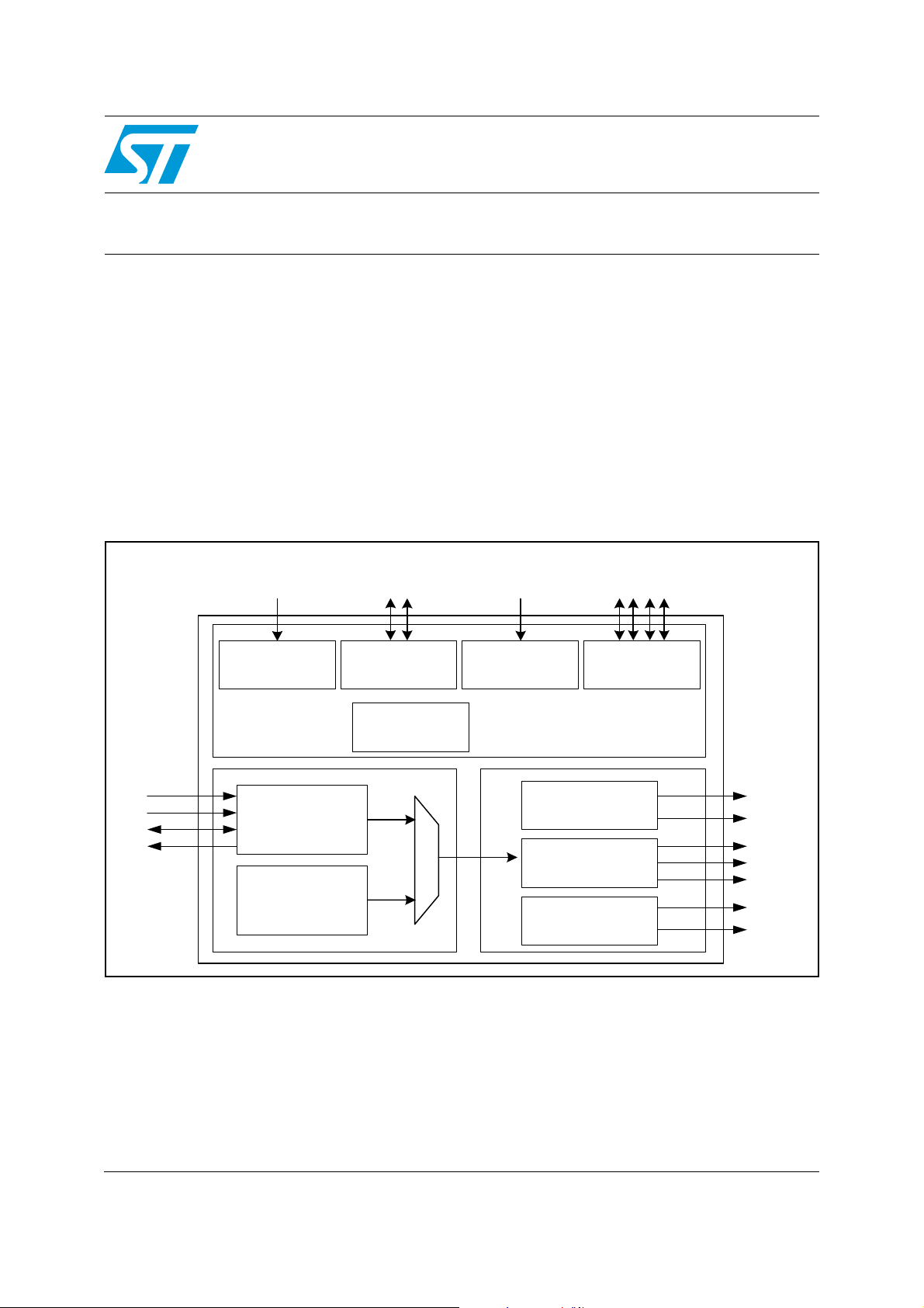
27 MHz
Crystal
Clock
Generator
SPI Flash
SPI
Controller
OCM
■ Sink detection logic
■ Low power operation – Active 400mW, standby
mode 15mW
■ Package: 64-pin LQFP, 10 x 10 mm
Applications
■ DisplayPort to VGA dongle as an attachment to
Notebook and Desktop PCs
■ DisplayPort to VGA conversion for Notebook
and Desktop PC motherboard applications
Reset
Reset
Circuit
GPIO
L0
L1
AUX
HPD
2 Lane
DisplayPort
Receiver
Pattern
Generator
HSYNC, VSYNC
Gen
DAC 10-bit color
DDC
HSYNC
VSYNC
Red
Green
Blue
DDC SDA
DDC SCL
November 2008 Rev 1 1/7
For further information contact your local STMicroelectronics sales office.
www.st.com
7
Page 2
Description STDP3100
1 Description
STDP3100 is a DisplayPort to VGA signal format converter for interfacing next generation
DisplayPort based PC and notebook computers with conventional VGA displays, such as
CRT, LCD monitors, and projectors. DisplayPort offers a unified, scalable, and cost effective
interface for embedded and external display applications. As desktop and notebook PCs are
increasingly transitioning from conventional analog type interfaces to DisplayPort,
STDP3100 facilitates the transition by offering seamless connectivity between new
DisplayPort PC and notebooks and the installed base VGA monitors and projectors.
STDP3100 is a highly integrated converter featuring a DisplayPort receiver, video DAC,
clock form generator, test pattern generator, and sink detection block. In addition,
STDP3100 includes EDID and MCCS pass-through features, forming a fully transparent
operation between the PC and display. Active power consumption of this device is as low as
400mW, and thus it can be powered by the DisplayPort source when used in dongle
application. The device has a built in sink detection feature that determines the active and
standby state. The device enters into standby (low power) state whenever the VGA cable is
disconnected and returns to normal operation when the cable is connected back.
STDP3100 supports video resolutions from VGA through WUXGA. The input DisplayPort
interface consists of two main lanes, AUX channel, and HPD signal that maps directly to a
standard DisplayPort connector via two layers PCB. The output interface consists of analog
R, G, B video, Hsync, Vsync, and DDC signals. Analog video signal amplitude ranges from 0
to 700mV from a 10 bit video DAC with maximum sampling frequency of 162 MHz. The VGA
output signal interface conforms to the VSIS standards with separate Hsync and Vsync
control signals. The DDC_SDA and DDC_CLK signals are driven from an I2C master, which
controls I2C traffic between the DisplayPort AUX channel and external slave device.
ST offers STDP3100 designers kit with complete reference hardware and firmware.
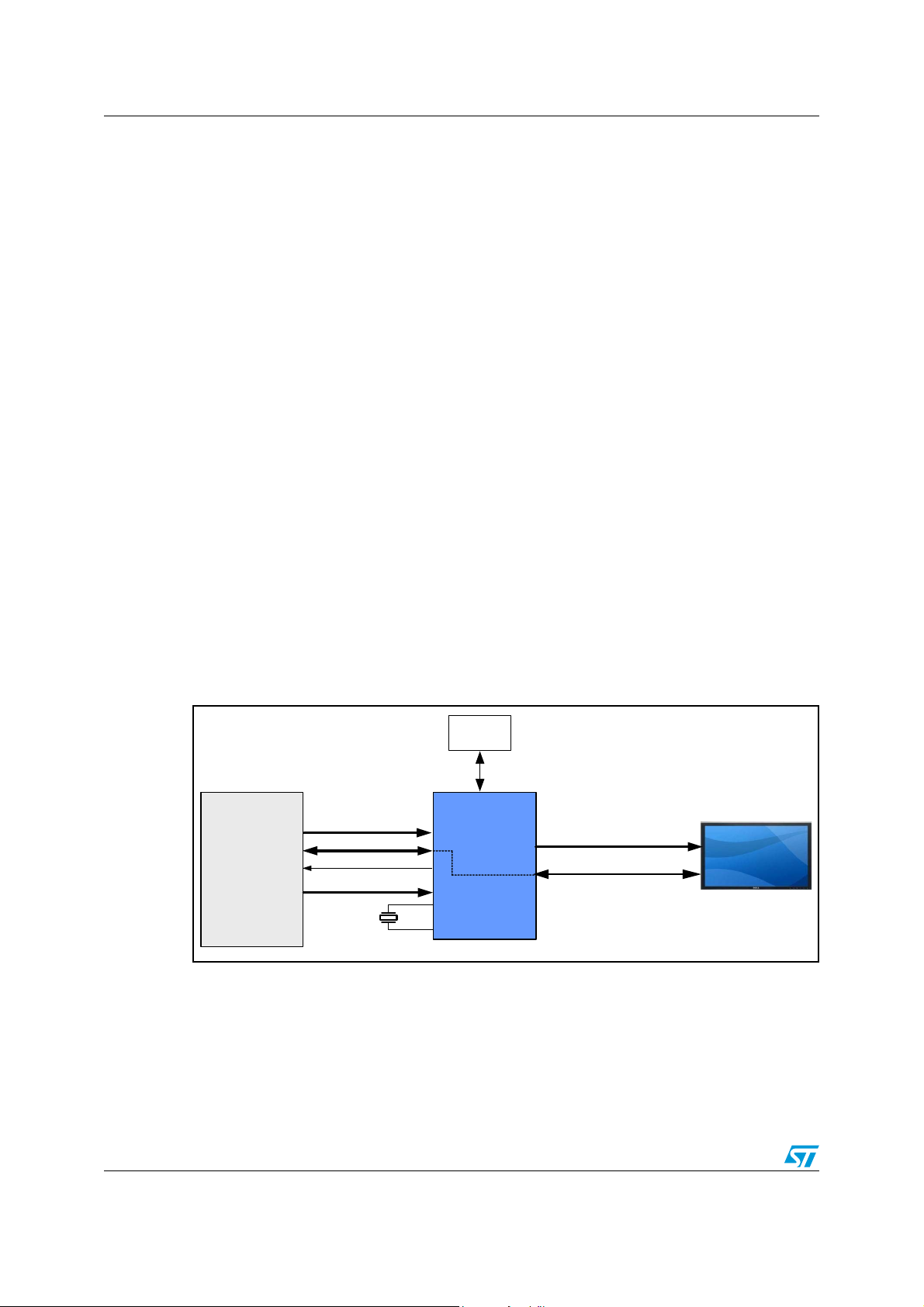
Figure 1. System diagram
SPI
Flash
SPI
Display
DP
Source
Main Link
AUX CH
HPD_out
3.3V from DP connector
27.000 MHz
Crystal
STDP3100
TCLK
XCLK
I2C maste r
Analog R,G,B
and Hsync, Vsync
DDC
2/7
Page 3

STDP3100 Benefits
2 Benefits
● Production-proven DisplayPort receiver from the DisplayPort leader
● Comprehensive feature set for DisplayPort to VGA dongle and for notebook embedded
application
● Proven interoperability with DisplayPort sources from all major graphics vendors
● Cost savings due to optimized BOM, low power, low EMI, and small form factor
● DisplayPort CTS compliant
3/7
Page 4

Feature attributes STDP3100
3 Feature attributes
● DisplayPort 1.1a compliant receiver offering 5.4 Gbps bandwidth over 2 lanes
● Integrated triple 10-bit, 162 MHz video DAC for analog VGA signal output
● Supports up to 1080p, 1920 x 1200 reduced blanking video resolution
● EDID and MCCS pass-through from PC source to display
● Spread Spectrum (de-spreading) for EMI reduction
● Automatic sink detection
● Low power standby mode operation initiated based on sink detection status
● SPI interface with external Serial Flash for storing firmware and system configuration
data for customization purposes
● Optional two-wire host interface for device configuration using external controller
● UART interface for chip debug and development purposes
● ISP over DP AUX channel
● General purpose I/O pins for system usage
● Powered from DisplayPort source
● 3.3V IO, 1.2V Core
● 64-pin LQFP (10 x 10 mm) package
4/7
Page 5

STDP3100 Ordering information
4 Ordering information
b
Table 1. Order codes
Part number Description
STDP3100 64-pin LQFP
(10 x 10 mm) Lead Free
5/7
Page 6

Revision history STDP3100
5 Revision history
Table 2. Document revision history
Date Revision Changes
4-Nov-2008 1 Initial release.
6/7
Page 7

STDP3100
Please Read Carefully:
Information in this document is provided solely in connection with ST products. STMicroelectronics NV and its subsidiaries (“ST”) reserve the
right to make changes, corrections, modifications or improvements, to this document, and the products and services described herein at any
time, without notice.
All ST products are sold pursuant to ST’s terms and conditions of sale.
Purchasers are solely responsible for the choice, selection and use of the ST products and services described herein, and ST assumes no
liability whatsoever relating to the choice, selection or use of the ST products and services described herein.
No license, express or implied, by estoppel or otherwise, to any intellectual property rights is granted under this document. If any part of this
document refers to any third party products or services it shall not be deemed a license grant by ST for the use of such third party products
or services, or any intellectual property contained therein or considered as a warranty covering the use in any manner whatsoever of such
third party products or services or any intellectual property contained therein.
UNLESS OTHERWISE SET FORTH IN ST’S TERMS AND CONDITIONS OF SALE ST DISCLAIMS ANY EXPRESS OR IMPLIED
WARRANTY WITH RESPECT TO THE USE AND/OR SALE OF ST PRODUCTS INCLUDING WITHOUT LIMITATION IMPLIED
WARRANTIES OF MERCHANTABILITY, FITNESS FOR A PARTICULAR PURPOSE (AND THEIR EQUIVALENTS UNDER THE LAWS
OF ANY JURISDICTION), OR INFRINGEMENT OF ANY PATENT, COPYRIGHT OR OTHER INTELLECTUAL PROPERTY RIGHT.
UNLESS EXPRESSLY APPROVED IN WRITING BY AN AUTHORIZED ST REPRESENTATIVE, ST PRODUCTS ARE NOT
RECOMMENDED, AUTHORIZED OR WARRANTED FOR USE IN MILITARY, AIR CRAFT, SPACE, LIFE SAVING, OR LIFE SUSTAINING
APPLICATIONS, NOR IN PRODUCTS OR SYSTEMS WHERE FAILURE OR MALFUNCTION MAY RESULT IN PERSONAL INJURY,
DEATH, OR SEVERE PROPERTY OR ENVIRONMENTAL DAMAGE. ST PRODUCTS WHICH ARE NOT SPECIFIED AS "AUTOMOTIVE
GRADE" MAY ONLY BE USED IN AUTOMOTIVE APPLICATIONS AT USER’S OWN RISK.
Resale of ST products with provisions different from the statements and/or technical features set forth in this document shall immediately void
any warranty granted by ST for the ST product or service described herein and shall not create or extend in any manner whatsoever, any
liability of ST.
ST and the ST logo are trademarks or registered trademarks of ST in various countries.
Information in this document supersedes and replaces all information previously supplied.
The ST logo is a registered trademark of STMicroelectronics. All other names are the property of their respective owners.
© 2008 STMicroelectronics - All rights reserved
STMicroelectronics group of companies
Australia - Belgium - Brazil - Canada - China - Czech Republic - Finland - France - Germany - Hong Kong - India - Israel - Italy - Japan -
Malaysia - Malta - Morocco - Singapore - Spain - Sweden - Switzerland - United Kingdom - United States of America
www.st.com
7/7
 Loading...