

1
3
1
3
3
查询STP5NK60Z供应商
N-CHANNEL 650V @Tjmax - 1.2Ω - 5A TO-220/FP/DPAK
STD5NK60Z
STP5NK60Z - STP5NK60ZFP
Zener-Protected SuperMESH™ MOSFET
Table 1: General Features
TYPE V
STP5NK60Z
STP5NK60ZFP
STD5NK60Z
■ TYPICAL R
■ EXTREMELY HIGH dv /d t CAPABILITY
■ 100% AVALANCHE TESTED
■ GATE CHARGE MINIMIZED
■ VERY LOW INTRINSIC CAPACITANCES
■ VERY GOOD MANUFACTURING
DS
@
DSS
TJmax
650 V
650 V
650 V
R
< 1.6 Ω
< 1.6 Ω
< 1.6 Ω
(on) = 1.2 Ω
DS(on)
I
5 A
5 A
5 A
P
d
TOT
90 W
25 W
90 W
REPEATIBILITY
DESCRIPTION
The SuperMESH™ series is obtained through an
extreme optimization of ST’s well established
strip-based PowerMESH™ layout. In addition to
pushing on-resistance significantly down, special
care is taken to ensure a very good dv/dt capability
for the most demanding applications. Such series
complements ST full range of high voltage MOS
-
FET s including revolutionary MDmesh™ products.
APPLICATIONS
■ HIGH CURRENT, HIGH SPEED SWITCHING
■ IDEAL F OR OFF-LINE POW E R SUPP L IES,
ADAPTORS AND PFC
■ LIGHTING
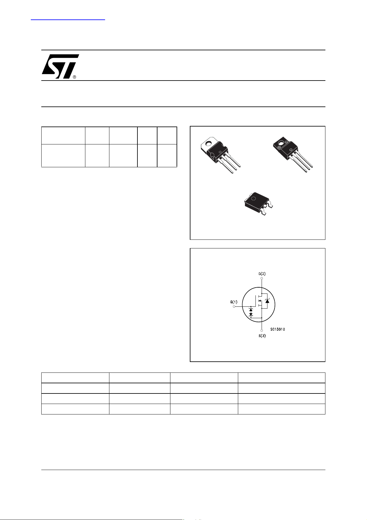
Figure 1: Package
2
TO-220
TO-220FP
1
DPAK
Figure 2: Internal Schematic Diagram
2
Table 2: Order Codes
SALES TYPE MARKING PACKAGE PACKAGING
STP5NK60Z P5NK60Z TO-220 TUBE
STP5NK60ZFP P5NK60ZFP TO-220FP TUBE
STD5NK60ZT4 D5NK60 DPAK TAPE & REEL
Rev. 7
1/14December 2005
STP5NK60Z - STP5NK60ZFP- STD5NK60Z
Table 3: Absolute Maximum ratings
Symbol Parameter Value Unit
TO-220/DPAK TO-220FP
V
DS
V
DGR
V
GS
I
D
I
D
I
DM
P
TOT
V
ESD(G-S)
dv/dt (1) Peak Diode Recovery voltage slope 4.5 V/ns
V
ISO
T
j
T
stg
(z) Pulse width l i m i ted by safe operating area
(1) ISD ≤5A, di/dt ≤200A/µs, VDD ≤ V
(*) Limited only by maximum temperature allowed
Drain-source Voltage (VGS = 0)
Drain-gate Voltage (RGS = 20 kΩ)
600 V
600 V
Gate- source Voltage ± 30 V
Drain Current (continuous) at TC = 25°C
Drain Current (continuous) at TC = 100°C
(z)
Drain Current (pulsed) 20 20 (*) A
Total Dissipation at TC = 25°C
5 5 (*) A
3.16 3.16 (*) A
90 25 W
Derating Factor 0.72 0.2 W/°C
Gate source ESD(HBM-C=100pF, R=1.5KΩ) 3000 V
Insulation Withstand Voltage (DC) - 2500 V
Operating Junction Temperature
Storage Temperature
, Tj ≤ T
(BR)DSS
JMAX.
-55 to 150 °C
Thermal Data
TO-220/DPAK TO-220FP
Rthj-case Thermal Resistance Junction-case Max 1.39 5 °C/W
Rthj-amb Thermal Resistance Junction-ambient Max 62.5 °C/W
T
l
(#) When mount ed on 1inch² FR-4, 2 Oz c opper board.
Maximum Lead Temperature For Soldering Purpose 300
°C
Table 4: Avalanche Characteristics
Symbol Parameter Max Value Unit
I
AR
Avalanche Current, Repetitive or Not-Repetitive
5 A
(pulse width limited by Tj max)
E
AS
Single Pulse Avalanche Energy
220 mJ
(starting Tj = 25 °C, ID = IAR, VDD = 50 V)
Table 5: Gate-Source Zener Diode
Symbol Parameter Test Conditions Min. Typ. Max. Unit
BV
GSO
Gate-Source Breakdown
Igs=± 1mA (Open Drain) 30 V
Voltage
PROTECTION FEATURES OF GATE-TO-SOURCE ZEN E R DIODES
The built-in back-to-back Zener diodes have sp ecifically been desig ned to enhance not only the dev ice’s
ESD capability, but also to make them safely absorb possible voltage transients that may occasionally be
applied from gate to source. In this respect the Zener voltage is appropriate to achieve an ef ficient and
cost-effective intervention t o protec t t he d ev ice’s i ntegrity. T hese integrated Zener d iodes thu s av oid the
usage of external components.
2/14
STP5NK60Z - STP5NK60Z FP- STD5NK60Z
ELECTRICAL CHARACTERISTICS (T
=25°C UNLESS OTHERWISE SPECIFIED)
CASE
Table 6: On/Off
Symbol Parameter Test Conditions Min. Typ. Max. Unit
V
(BR)DSS
Drain-source
ID = 1 mA, VGS = 0 600 V
Breakdown Voltage
I
DSS
I
GSS
Zero Gate Voltage
Drain Current (VGS = 0)
Gate-body Leaka ge
VDS = Max Rating
VDS = Max Rating, TC = 125 °C
1
50
VGS = ± 20V ±10 µA
Current (VDS = 0)
V
GS(th)
R
DS(on)
Gate Threshold Voltage
Static Drain-source On
VDS = VGS, ID = 50µA
3 3.75 4.5 V
VGS = 10V, ID = 2.5 A 1.2 1.6 Ω
Resistance
Table 7: Dynamic
Symbol Parameter Test Conditions Min. Typ. Max. Unit
g
(1) Forward Transconductance VDS = 8 V, ID = 2.5 A 4 S
fs
C
oss eq.
C
iss
C
oss
C
rss
t
d(on)
t
t
d(off)
t
t
r(Voff)
t
t
Q
Q
Q
r
r
f
c
g
gs
gd
Input Capacitance
Output Capacitance
Reverse Transfer
Capacitance
(3) Equivalent Outpu t
Capacitance
Turn-on Delay Time
Rise Time
Turn-off Delay Time
Fall Time
Off-voltage Rise Time
Fall Time
Cross-over Time
Total Gate Charge
Gate-Source Charge
Gate-Drain Charge
VDS = 25V, f = 1 MHz, VGS = 0 690
90
20
VGS = 0V, VDS = 0V to 480V 40 pF
VDD = 300 V, ID = 2.5 A
RG = 4.7Ω VGS = 10 V
(see Figure 20)
16
25
36
25
VDD = 480V, ID = 5 A,
RG = 4.7Ω, V
GS
= 10V
(see Figure 20)
VDD = 400V, ID = 5 A,
VGS = 10V
(see Figure 23)
12
10
24
26
20
34 nC
6
µA
µA
pF
pF
pF
ns
ns
ns
ns
ns
ns
ns
nC
nC
Table 8: Source Drain Diode
Symbol Parameter Test Conditions Min. Typ. Max. Unit
I
SD
I
(2)
SDM
VSD (1)
t
rr
Q
rr
I
RRM
Note: 1. Pulsed: P ul se duration = 300 µs, d ut y cy cle 1.5 %.
2. Pulse wi dt h l i m ited by safe op erating area.
3. C
Source-drain Current
Source-drain Current (pulsed)
Forward On Voltage
Reverse Recovery Time
Reverse Recovery Charge
Reverse Recovery Current
is defined as a constant equivalent capacitance giving the same charging time as C
oss eq.
.
V
DSS
ISD = 5 A, VGS = 0
ISD = 5 A, di/dt = 100A/µs
VDD = 30V, Tj = 150°C
(see Figure 21)
485
2.7
11
when VDS increases from 0 to 80%
oss
5
20
1.6 V
A
A
ns
µC
A
3/14
STP5NK60Z - STP5NK60ZFP- STD5NK60Z
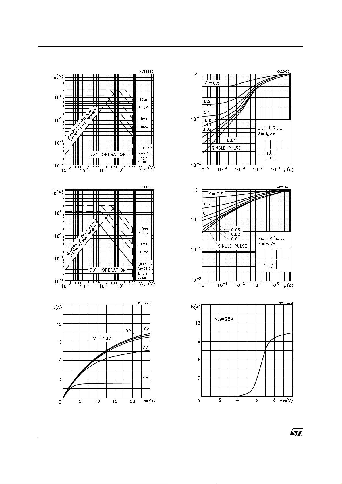
Figure 3: Safe Operating Area For TO-220/
DPAK
Figure 4: Safe Operating Area For TO-220FP
Figure 6: Thermal Impedance For TO-220/
DPAK
Figure 7: Thermal Impedance For TO-220FP
Figure 5: Output Characteristics
4/14
Figure 8: Transfer Characteristics
STP5NK60Z - STP5NK60Z FP- STD5NK60Z
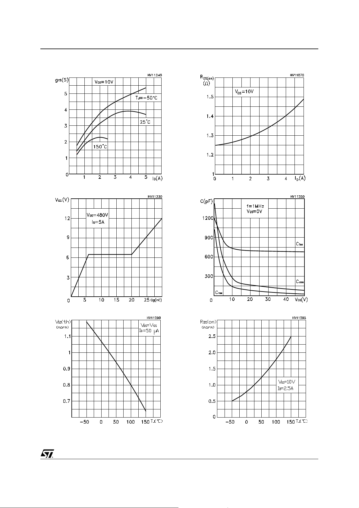
Figure 9: Transconductance
Figure 10: Gate Charge vs Gate-source Voltage
Figure 12: Static Drain-source On Resistance
Figure 13: Capacitance Variations
Figure 11: Normalized Gate Threshold Voltage
vs Tem pera tur e
Figure 14: Normal ized On R esistance vs Temperature
Figure 15:
5/14

STP5NK60Z - STP5NK60ZFP- STD5NK60Z
Figure 16: S ource-Drain Forward Char acteristics
Figure 17: Maximum Avalanche Energy vs
Temperature
Figure 18: Normalized BVdss vs Temperature
6/14

STP5NK60Z - STP5NK60Z FP- STD5NK60Z
Figure 19: Unclamped Inductive Load Test Circuit
Figure 20: Switching Times Test Circuit For
Resistive Load
Figure 22: Unclamped Inductive Wafeform
Figure 23: Gate Charge Test Circuit
Figure 21: Test Circuit For Inductive Load
Switching and Diode Recovery Times
7/14

STP5NK60Z - STP5NK60ZFP- STD5NK60Z
In order to meet environmental requirements, ST offers these devices in ECOPACK® packages. These
packages have a Lead-free second level interconnect . The category of second level interconnect is
marked on the package and on the inner box label, i n compliance with JEDEC Standard JESD97. The
maximum ratings related to soldering conditions are also marked on the inner box label. ECOPACK is an
ST trademark. ECOPACK specifications are available at:
www.st.com
8/14

STP5NK60Z - STP5NK60Z FP- STD5NK60Z
TO-220 MECHANICAL DATA
DIM.
A 4.40 4.60 0.173 0.181
b 0.61 0.88 0.024 0.034
b1 1.15 1.70 0.045 0.066
c 0.49 0.70 0.019 0.027
D 15.25 15.75 0.60 0.620
E 10 10.40 0.393 0.409
e 2.40 2.70 0.094 0.106
e1 4.95 5.15 0.194 0.202
F 1.23 1.32 0.048 0.052
H1 6.20 6.60 0.244 0.256
J1 2.40 2.72 0.094 0.107
L 13 14 0.511 0.551
L1 3.50 3.93 0.137 0.154
L20 16.40 0.645
L30 28.90 1.137
øP 3.75 3.85 0.147 0.151
Q 2.65 2.95 0.104 0.116
MIN. TYP MAX. MIN. TYP. MAX.
mm. inch
9/14

STP5NK60Z - STP5NK60ZFP- STD5NK60Z
TO-220FP MECHANICAL DATA
DIM.
A 4.4 4.6 0.173 0.181
B 2.5 2.7 0.098 0.106
D 2.5 2.75 0.098 0.108
E 0.45 0.7 0.017 0.027
F 0.75 1 0.030 0.039
F1 1.15 1.7 0.045 0.067
F2 1.15 1.7 0.045 0.067
G 4.95 5.2 0.195 0.204
G1 2.4 2.7 0.094 0.106
H 10 10.4 0.393 0.409
L2 16 0.630
L3 28.6 30.6 1.126 1.204
L4 9.8 10.6 .0385 0.417
L5 2.9 3.6 0.114 0.141
L6 15.9 16.4 0.626 0.645
L7 9 9.3 0.354 0.366
Ø 3 3.2 0.118 0.126
MIN. TYP MAX. MIN. TYP. MAX.
mm. i nch
10/14
E
A
D
B
L3
L6
L7
F1
H
F
1
G
G
F2
123
L2
L5
L4

STP5NK60Z - STP5NK60Z FP- STD5NK60Z
TO-252 (DPAK) MECHANICAL DATA
DIM.
A 2.20 2.40 0.087 0.094
A1 0.90 1.10 0.035 0.043
A2 0.03 0.23 0.001 0.009
B 0.64 0.90 0.025 0.035
B2 5.20 5.40 0.204 0.213
C 0.45 0.60 0.018 0.024
C2 0.48 0.60 0.019 0.024
D 6.00 6.20 0.236 0.244
E 6.40 6.60 0.252 0.260
G 4.40 4.60 0.173 0.181
H 9.35 10.10 0.368 0.398
L2 0.8 0.031
L4 0.60 1.00 0.024 0.039
V2 0
MIN. TYP. MAX. MIN. TYP. MAX.
o
mm inch
o
8
o
0
o
0
P032P_B
11/14
STP5NK60Z - STP5NK60ZFP- STD5NK60Z
DPAK FOOTPRINT
All dimensions are in millimeters
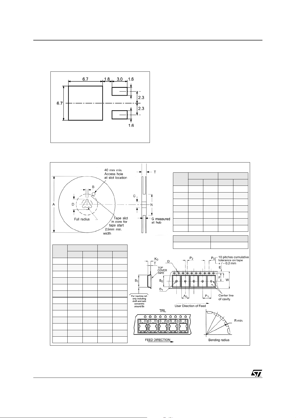
TAPE AND REEL SHIPMENT
REEL MECHANICAL DATA
DIM.
A 330 12.992
B 1.5 0.059
C 12.8 13.2 0.504 0.520
D 20.2 0.795
G 16.4 18.4 0.645 0.724
N 50 1.968
T 22.4 0.881
mm inch
MIN. MAX. MIN. MAX.
12/14
TAPE MECHANICAL DATA
DIM.
A0 6.8 7 0.267 0.275
B0 10.4 10.6 0.409 0.417
B1 12.1 0.476
D 1.5 1.6 0.059 0.063
D1 1.5 0.059
E 1.65 1.85 0.065 0.073
F 7.4 7.6 0.291 0.299
K0 2.55 2.75 0.100 0.108
P0 3.9 4.1 0.153 0.161
P1 7.9 8.1 0.311 0.319
P2 1.9 2.1 0.075 0.082
R 40 1.574
W 15.7 16.3 0.618 0.641
mm inch
MIN. MAX. MIN. MAX.
BASE QTY BULK QTY
2500 2500

Table 9: Revision History
Date Revision Descrip tion of Change s
05-Apr-2005 1 First issue
29-Apr-2005 2 Modified value in Table 7.
06-Sep-2005 3 Inserted Ecopack indication
14-Oct-2005 4 Modified value on Table 1
28-Oct-2005 5 Tape & Reel info added
14-Nov-2005 6 Modified value on Table 6
15-Dec-2005 7 Various corrections
STP5NK60Z - STP5NK60Z FP- STD5NK60Z
13/14

STP5NK60Z - STP5NK60ZFP- STD5NK60Z
I
s
o
d
b
t
t
t
a
nformation furnished is believed to be accurate and reliable. However, STMicroelectronics assumes no responsibility for the consequence
f use of such information nor for any infringement of patents or other rights of third parties which may result from its use. No license is grante
y implicat io n or ot h er wis e under an y pat e nt or pa te nt r igh ts of STMi c roe l ec tro ni c s. Sp ec i fi ca ti on s ment i o ne d in th is p ub li c ati on ar e s ub jec
o change without noti ce. This publication supersedes and replaces all information previously supplied. STMicroelectronics pro d ucts are no
uthorized for use as critical components in life support devices or systems without express written approval of STMicroelectronics.
The ST logo is a registered trademark of STMicroelectronics
All other names are the property of their respective owners
© 2005 STMicroelectronics - All Rights Reserved
STMicroelectronics group of companies
Australia - Belgium - Brazil - Canada - China - Czech Republic - Finland - France - Germany - Hong Kong - India - Israel - Italy - Japan -
Malaysia - Malta - Morocco - Singapore - Spain - Sweden - Switzerland - United Kingdom - United States of America
14/14

WWW.ALLDATASHEET.COM
Copyright © Each Manufacturing Company.
All Datasheets cannot be modified without permission.
This datasheet has been download from :
www.AllDataSheet.com
100% Free DataSheet Search Site.
Free Download.
No Register.
Fast Search System.
www.AllDataSheet.com
 Loading...