

ST STQ2HNK60ZR-AP, STF2HNK60Z, STD2HNK60Z-1 User Manual
查询STD2HNK60Z-1供应商
N-CHANNEL 600V - 4.4Ω - 2.0A TO-92/TO-220FP/IPAK
STQ2HNK60ZR-AP
STF2HNK60Z - STD2HNK60Z-1
Zener-Protected SuperMESH™ MOSFET
TYPE V
STQ2HNK60ZR-AP
STD2HNK60Z-1
STF2HNK60Z
TYPICAL RDS(on) = 4.4Ω
EXTREMELY HIGHdv/dt CAPABILITY
ESD IMPROVED CAPABILITY
100% AVALANCHE TESTED
NEW HIGH VOLTAGE BENCHMARK
GATE CHARGE MINIMIZED
600 V
600 V
600 V
DSS
R
DS(on)
<4.8Ω
<4.8Ω
<4.8Ω
I
D
0.5 A
2.0 A
2.0 A
P
W
3W
45 W
20 W
DESCRIPTION
The SuperMESH ™ series is obtained through an
extreme optimization of ST’s well established stripbased PowerMESH™ layout. In addition to pushing
on-resistance significantly down,specialcareis taken to ensure a very good dv/dt capability for the
most dem anding applications. Such series complements ST full range of high voltage MOSFETs including revolutionary MDm es h™ products.
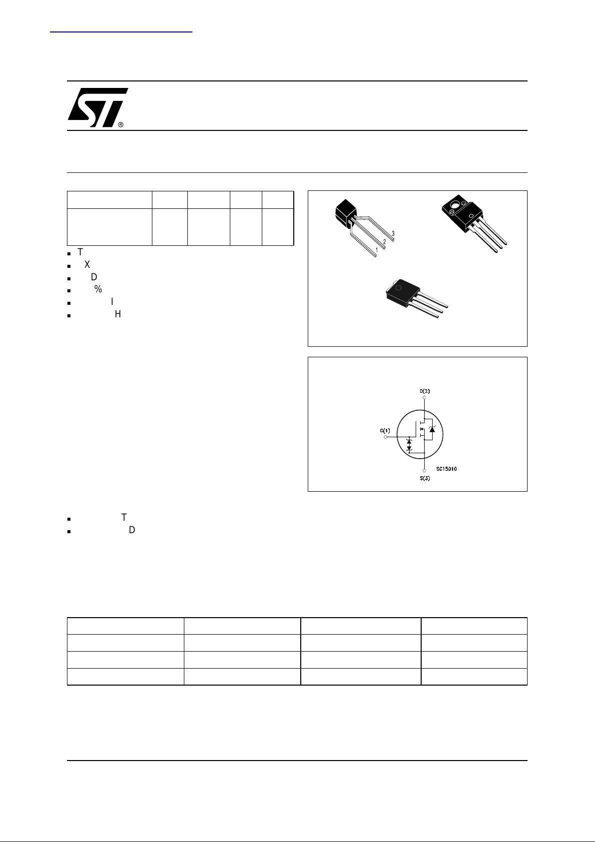
TO-92 (Ammopack)
TO-220FP
3
2
1
IPAK
INTERNAL SCHEMATIC DIAGRAM
3
2
1
APPLICATIONS
AC ADAPTORS AND BATTERY CHARGERS
SWITH MODE POWER SUPPLIES (SMPS)
ORDER CODES
PART NUMBER MARKING PACKAGE PACKAGING
STD2HNK60Z-1 D2HNK60Z IPAK TUBE
STQ2HNK60ZR-AP Q2HNK60ZR TO-92 AMMOPAK
STF2HNK60Z F2HNK60Z TO-220FP TUBE
1/12April 2004
STQ2HNK60ZR-AP - STF2HNK 60Z - STD2HNK60Z-1
ABSOLUTE MAXIMUM RATINGS
Symbol Parameter Value Unit
IPAK TO-220FP TO-92
V
DS
V
DGR
V
GS
I
D
I
D
I
DM
P
TOT
V
ESD(G-S)
dv/dt (1) Peak Diode Recovery voltage slope 4.5 V/ns
V
ISO
T
j
T
stg
() Pulse width limited by safe operating area
≤ 2A,di/dt≤ 200 A/µs, VDD≤ V
(1) I
SD
(*)Current Limitedbypackage
Drain-source Voltage (VGS=0)
Drain-gate Voltage (RGS=20kΩ)
600 V
600 V
Gate- source Voltage ± 30 V
Drain Current (continuous) at TC=25°C
Drain Current (continuous) at TC= 100°C
()
Drain Current (pulsed) 8 8 (*) 2 A
Total Dissipation at TC=25°C
2.0 2.0 (*) 0.5 A
1.26 1.26 (*) 0.32 A
45 20 3 W
Derating Factor 0.36 0.16 0.025 W/°C
Gate source ESD(HBM-C=100pF, R=1.5KΩ) 2000 V
Insulation Withstand Voltage (DC) -- 2500 -- V
Operating Junction Temperature
Storage Temperature
(BR)DSS,Tj
≤ T
JMAX.
-55 to 150 °C
THERMAL DATA
IPAK TO-220FP TO-92
Rthj-case Thermal Resistance Junction-case Max 2.77 6.25 -- °C/W
Rthj-amb Thermal Resistance Junction-ambient Max 100 62.5 120 °C/W
Rthj-lead Thermal Resistance Junction-lead Max -- -- 40 °C/W
T
Maximum Lead Temperature For Soldering
l
300 300 260 °C
Purpose
AVALANCHE CHARACTERISTICS
Symbol Parameter Max Value Unit
I
AR
E
AS
Avalanche Current, Repetitive or Not-Repetitive
(pulse width limited by T
max)
j
Single Pulse Avalanche Energy
(starting T
=25°C, ID=IAR,VDD=50V)
j
2A
120 mJ
GATE-SOURCE ZENER DIODE
Symbol Parameter Test Conditions Min. Typ. Max. Unit
BV
GSO
Gate-Source Breakdown
Voltage
Igs=± 1mA (Open Drain) 30 V
PROTECTION FEATURES OF GATE-TO-SOURCE ZENER DIODES
The built-in back-to-back Zener diodes hav e specifically been designed to enhance not only the device’s
ESD capability, but also to make them sa fely absorb possible voltage transients that may occasionally be
applied from gate to source. In this respect the Zener voltage is appropriate to achieve an efficient and
cost-effective intervention to prote ct the device’s integrity. These integrated Zener diodes thus avoid the
usage of external components.
2/12
STQ2HNK60ZR-AP - STF2HNK60Z - STD2HNK60Z-1
ELECTRICAL CHARACTERISTICS (T
=25°C UNLESS O THERWISE SPECIFIED)
CASE
ON/OFF
Symbol Parameter Test Conditions Min. Typ. Max. Unit
V
(BR)DSS
Drain-source
ID=1mA,VGS= 0 600 V
Breakdown Voltage
I
I
GSS
V
GS(th)
R
DS(on)
DSS
Zero Gate Voltage
Drain Current (V
GS
=0)
Gate-body Leakage
Current (V
DS
=0)
Gate Threshold Voltage
Static Drain-source On
V
=MaxRating
DS
=MaxRating,TC= 125 °C
V
DS
V
= ± 20V ±10 µA
GS
V
DS=VGS,ID
=50µA
3 3.75 4.5 V
1
50
VGS=10V,ID= 1.0 A 4.4 4.8 Ω
Resistance
DYNAMIC
Symbol Parameter Test Conditions Min. Typ. Max. Unit
g
(1) Forward Transconductance VDS=15V,ID= 1.0 A 1.5 S
fs
C
oss eq.
C
C
C
t
d(on)
t
d(off)
Q
Q
Q
iss
oss
rss
t
t
gd
r
f
g
gs
Input Capacitance
Output Capacitance
Reverse Transfer
Capacitance
(3) Equivalent Output
Capacitance
Turn-on Delay Time
Rise Time
Turn-off Delay Time
Fall Time
Total Gate Charge
Gate-Source Charge
Gate-Drain Charge
=25V,f=1MHz,VGS= 0 280
V
DS
38
7
VGS=0V,VDS= 0V to 480V 30 pF
=300V,ID=1.0A
V
DD
R
=4.7Ω VGS=10V
G
(Resistive Load see, Figure 3)
10
30
23
50
=480V,ID=2.0A,
V
DD
VGS=10V
11
2.25
15
6
µA
µA
pF
pF
pF
ns
ns
ns
ns
nC
nC
nC
SOURCE DRAIN DIODE
Symbol Parameter Test Conditions Min. Typ. Max. Unit
I
SD
I
SDM
VSD(1)
t
rr
Q
rr
I
RRM
t
rr
Q
rr
I
RRM
Note: 1. Pulsed: Pulse duration = 300 µs, duty cycle 1.5 %.
2. Pulse width limited by safe operating area .
3. C
Source-drain Current
(2)
Source-drain Current (pulsed)
ForwardOnVoltage
Reverse Recovery Time
Reverse Recovery Charge
Reverse Recovery Current
Reverse Recovery Time
Reverse Recovery Charge
Reverse Recovery Current
is defined as a constant equivalent capacitance giving the same charging time as C
oss eq.
.
V
DSS
ISD=2.0A,VGS=0
I
SD
V
DD
(see test circuit, Figure 5)
I
SD
V
DD
(see test circuit, Figure 5)
= 2.0 A, di/dt = 100 A/µs
=20V,Tj=25°C
=13A,di/dt=100A/µs
=20V,Tj= 150°C
178
445
5
200
500
5
when VDSincreases from 0 to 80%
oss
2.0
8.0
1.6 V
A
A
ns
nC
A
ns
nC
A
3/12
STQ2HNK60ZR-AP - STF2HNK 60Z - STD2HNK60Z-1
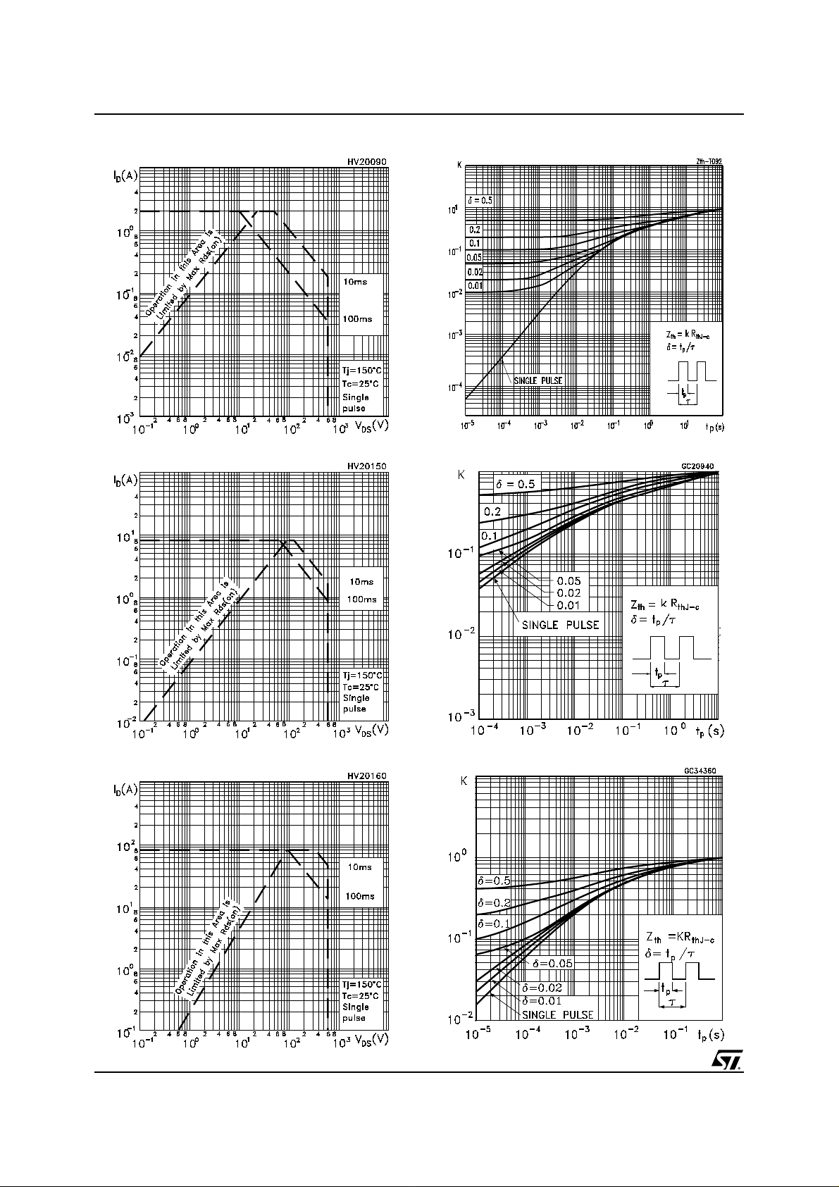
Thermal Impedance for TO-92Safe Operating Area for TO-92
Safe Operating Area for TO-220FP
Safe Operating Area for IPAK
Thermal Impedance for TO-220FP
Thermal Impedance for IPAK
4/12
 Loading...