

查询STD10NF06L供应商
STD10NF06L
N-CHANNEL 60V - 0.1Ω - 10A DPAK
STripFET™ POWER MOSFET
PRELIMINARY DATA
TYPE V
STD10NF06L 60V <0.12Ω 10A
■ TYPICAL R
■ SURFACE-MOUNTING DPAK (TO-252) POWER
DS
DSS
(on) = 0.1Ω
R
DS(on)
I
D
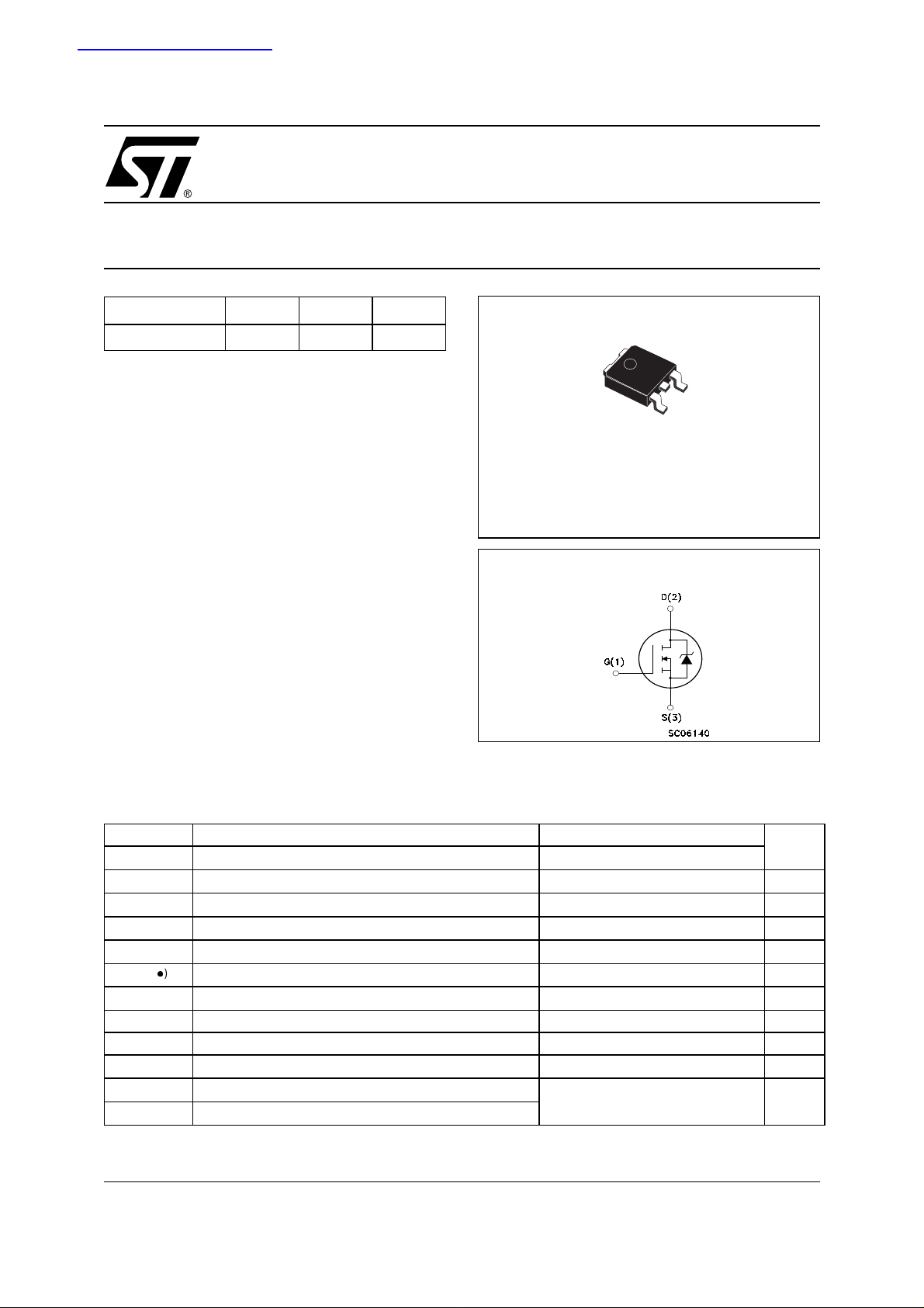
PACKAGE IN TAPE & REEL (SUFFIX “T4”)
DESCRIPTION
This MOSFET series realized with STMicroelectronics
unique STripFET
™ process has specifically been de-
signed to minimize input capacitance and gate charge.
It is therefore suitable as primary swi tch in advanced
high-efficiency, high-frequency isolated DC-DC converters for Telecom and Computer applications. It is
also intended for any applications with low gate drive
requirements.
APPLICATIONS
■ DC-DC & DC-AC CONVERTERS
■ DC MOTOR CONTROL
3
1
DPAK
INTERNAL SCHEMATIC DIAGRAM
ABSOLUTE MAXIMUM RATINGS
Symbol Parameter Value Unit
V
DS
V
DGR
V
GS
I
D
I
D
I
DM
P
TOT
dv/dt (1) Peak Diode Recovery voltage slope 30 V/ns
E
AS
T
stg
T
j
(●) Pulse width limited by safe operating area
November 2001
This is preliminary information on a new product now in development or undergoing evaluation. Details are subject to change without notice.
Drain-source Voltage (VGS = 0)
Drain-gate Voltage (RGS = 20 kΩ)
Gate- source Voltage ± 15 V
Drain Current (continuos) at TC = 25°C
Drain Current (continuos) at TC = 100°C
(l)
Drain Current (pulsed) 40 A
Total Dissipation at TC = 25°C
Derating Factor 0.2 W/°C
(2)
Single Pulse Avalanche Energy 50 mJ
Storage Temperature
Max. Operating Junction Temperature
(1) ISD ≤10A, di/dt ≤400A/µs, VDD =48V, Tj ≤ T
(2) Starting Tj = 25°C, Id = 7A, VDD=20 V
60 V
60 V
10 A
7A
30 W
– 55 to 175 °C
JMAX.
1/7
STD10NF06L
THERMA L D ATA
Rthj-case Thermal Resistance Junction-case Max 5 °C/W
Rthj-amb Thermal Resistance Junction-ambient Max 100 °C/W
T
l
ELECTRICAL CHARACTERISTICS (TCASE = 25 °C UNLESS OTHERWISE SPECIFIED)
OFF
Symbol Parameter Test Conditions Min. Typ. Max. Unit
V
(BR)DSS
I
DSS
I
GSS
ON
(1)
Symbol Parameter Test Conditions Min. Typ. Max. Unit
V
GS(th)
R
DS(on)
Maximum Lead Temperature For Soldering Purpose 275 °C
Drain-source
ID = 250 µA, VGS = 0 60 V
Breakdown Voltage
Zero Gate Voltage
Drain Current (V
GS
= 0)
Gate-body Leakage
Current (V
DS
= 0)
Gate Threshold Voltage
Static Drain-source On
Resistance
V
= Max Rating
DS
V
= Max Rating, TC = 125 °C
DS
V
= ± 15V ±100 nA
GS
V
= VGS, ID = 250µA
DS
VGS = 10V, ID = 5 A
VGS = 5 V, ID = 5 A
1V
0.1 0.12 Ω
0.12 0.14 Ω
1µA
10 µA
DYNAMIC
Symbol Parameter Test Conditions Min. Typ. Max. Unit
(1) Forward Transconductance VDS =15 V , ID=10A
g
fs
C
iss
C
oss
C
rss
Input Capacitance
Output Capacitance 54 pF
Reverse Transfer
Capacitance
V
= 25V, f = 1 MHz, VGS = 0
DS
6S
346 pF
22 pF
2/7

STD10NF06L
ELECTRICAL CHARACTERISTICS (CONTINUED)
SWITCHING ON
Symbol Parameter Test Conditions Min. Typ. Max. Unit
V
t
d(on)
Q
Q
Q
t
r
g
gs
gd
Turn-on Delay Time
Rise Time 50 ns
Total Gate Charge
Gate-Source Charge
Gate-Drain Charge
SWITCHING OFF
Symbol Parameter Test Conditions Min. Typ. Max. Unit
t
d(off)
t
f
Turn-off-Delay Time
Fall Time
SOURCE DRAIN DIODE
Symbol Parameter Test Conditions Min. Typ. Max. Unit
I
SD
I
SDM
VSD (1)
t
rr
Q
rr
I
RRM
Note: 1. Pulsed: Pu l se duration = 300 µs, duty c yc l e 1.5 %.
2. Pulse width li mited by safe operating area.
Source-drain Current 10 A
(2)
Source-drain Current (pulsed) 40 A
Forward On Voltage
Reverse Recovery Time
Reverse Recovery Charge
Reverse Recovery Current
= 30V, ID = 5A
DD
RG= 4.7Ω VGS = 4.5V
(see test circuit, Figure 3)
= 48V, ID = 10A,
V
DD
VGS = 5V
= 30V, ID = 5A,
V
DD
RG=4.7Ω, V
GS
= 4.5V
(see test circuit, Figure 5)
ISD = 10A, VGS = 0
= 10A, di/dt = 100A/µs,
I
SD
VDD = 20V, Tj = 150°C
(see test circuit, Figure 5)
10 ns
6
8
3
2.5
20
10
1.3 V
30
50
3
nC
nC
nC
ns
ns
ns
nC
A
3/7

STD10NF06L
Fig. 2: Unclamped Inductive WaveformFig. 1: Unclamped Inductive Load Test Circuit
Fig. 3: Switching Times Test Circuit For
Resistive Load
Fig. 5: Test Circuit For Inductive Load Switching
And Diode Recovery Times
Fig. 4: Gate Charge test Circuit
4/7

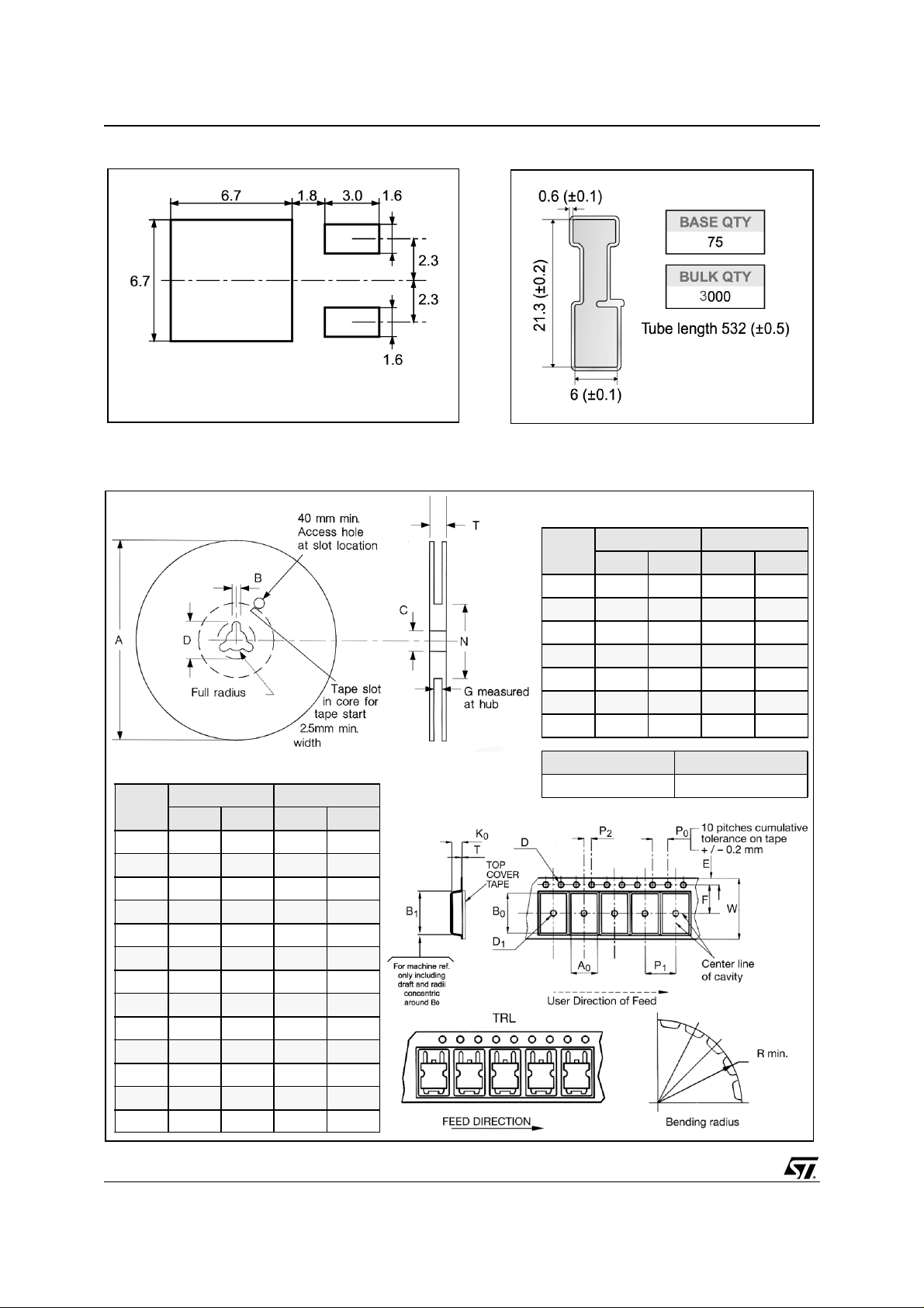
TO-252 (DPAK) MECHANICAL DATA
STD10NF06L
DIM.
A 2.20 2.40 0.087 0.094
A1 0.90 1.10 0.035 0.043
A2 0.03 0.23 0.001 0.009
B 0.64 0.90 0.025 0.035
B2 5.20 5.40 0.204 0.213
C 0.45 0.60 0.018 0.024
C2 0.48 0.60 0.019 0.024
D 6.00 6.20 0.236 0.244
E 6.40 6.60 0.252 0.260
G 4.40 4.60 0.173 0.181
H 9.35 10.10 0.368 0.398
L2 0.8 0.031
L4 0.60 1.00 0.024 0.039
V2 0
MIN. TYP. MAX. MIN. TYP. MAX.
o
mm inch
o
8
o
0
o
0
P032P_B
5/7
STD10NF06L
DPAK FOOTPRINT
All dimensions are in millimeters
TAPE AND REEL SHIPMENT (suffix ”T4”)*
TUBE SHIPMENT (no suffix)*
All dimensions
are in millimete rs
REEL MECHANICAL DATA
DIM.
A 330 12.992
B 1.5 0.059
C 12.8 13.2 0.504 0.520
D 20.2 0.795
G 16.4 18.4 0.645 0.724
N 50 1.968
T 22.4 0.881
mm inch
MIN. MAX. MIN. MAX.
TAPE MECHANICAL DATA
DIM.
A0 6.8 7 0.267 0.275
B0 10.4 10.6 0.409 0.417
B1 12.1 0.476
D 1.5 1.6 0.059 0.063
D1 1.5 0.059
E 1.65 1.85 0.065 0.073
F 7.4 7.6 0.291 0.299
K0 2.55 2.75 0.100 0.108
P0 3.9 4.1 0.153 0.161
P1 7.9 8.1 0.311 0.319
P2 1.9 2.1 0.075 0.082
R 40 1.574
W 15.7 16.3 0.618 0.641
* on s ales type
6/7
mm inch
MIN. MAX. MIN. MAX.
BASE QTY BULK QTY
1000 1000

STD10NF06L
Information furnished is believed to be accurate and reliable. However, STMicroelectronics assumes no responsibility for the consequences
of use of such informa tion n or for an y infring ement of patent s or other rig hts of third part ies which may resu lt from its use . No l i cen se i s
granted by implication or otherwise under any patent or patent rights of STMicroelectronics. Specification mentioned in this publication are
subject to change without notice. This publication supersedes and replaces all information previously supplied. STMicroelectronics products
are not authorized for use as critical compo nents in life support devices or systems without express written approval of STMicroelectronics.
Australia - Brazil - China - Finland - France - Germany - Hong Kong - India - Italy - Japan - Malaysia - Malta - Morocco -
The ST logo is a trademark of STMicroelectronics
© 2001 STMicroelectronics – Printed in Italy – All Rights Reserved
STMicroelectronics GROUP OF COMPANIES
Singapore - Spain - Sweden - Switzerland - United Kingdom - U.S.A.
http://www.st.com
7/7
 Loading...