

Features
■ Up to 40 V input voltage
■ Less than 0.5 V voltage overhead
■ Up to 2 A output current
■ PWM dimming pin
■ Shutdown pin
■ LED disconnection diagnostic
Applications
STCS2
2 A max constant current LED driver
10
1
PowerSO-10
■ LED constant current supplying for varying
input voltages
■ Low voltage lighting
■ Small appliances LED lighting
■ Car LED lights
Description
The STCS2 is a BiCMOS constant current source
designed to provide a precise constant current
starting from a varying input voltage source. The
main target is to replace discrete components
solution for driving LEDs in low voltage
applications such as 5 V, 12 V or 24 V giving
benefits in terms of precision, integration and
reliability.
The current is set with external resistor up to 2 A
with a ± 10 % precision; a dedicated pin allows
implementing PWM dimming.
An open-drain pin output provides information on
load disconnection condition.
Table 1. Device summary
Order code Package Packaging
STCS2SPR PowerSO-10 600 parts per reel
July 2008 Rev 4 1/16
www.st.com
16

Contents STCS2
Contents
1 Application diagram . . . . . . . . . . . . . . . . . . . . . . . . . . . . . . . . . . . . . . . . . 3
2 Pin configuration . . . . . . . . . . . . . . . . . . . . . . . . . . . . . . . . . . . . . . . . . . . 4
3 Maximum ratings . . . . . . . . . . . . . . . . . . . . . . . . . . . . . . . . . . . . . . . . . . . . 5
4 Electrical characteristics . . . . . . . . . . . . . . . . . . . . . . . . . . . . . . . . . . . . . 6
5 Timing . . . . . . . . . . . . . . . . . . . . . . . . . . . . . . . . . . . . . . . . . . . . . . . . . . . . . 7
6 Typical performance characteristics . . . . . . . . . . . . . . . . . . . . . . . . . . . . 8
7 Detail description . . . . . . . . . . . . . . . . . . . . . . . . . . . . . . . . . . . . . . . . . . . 9
7.1 Current setting . . . . . . . . . . . . . . . . . . . . . . . . . . . . . . . . . . . . . . . . . . . . . . 9
7.2 Enable . . . . . . . . . . . . . . . . . . . . . . . . . . . . . . . . . . . . . . . . . . . . . . . . . . . . 9
7.3 PWM dimming . . . . . . . . . . . . . . . . . . . . . . . . . . . . . . . . . . . . . . . . . . . . . . 9
7.4 Diagnostic . . . . . . . . . . . . . . . . . . . . . . . . . . . . . . . . . . . . . . . . . . . . . . . . . . 9
8 Application information . . . . . . . . . . . . . . . . . . . . . . . . . . . . . . . . . . . . . 10
8.1 Reverse polarity protection . . . . . . . . . . . . . . . . . . . . . . . . . . . . . . . . . . . . 10
8.2 Thermal considerations . . . . . . . . . . . . . . . . . . . . . . . . . . . . . . . . . . . . . . 10
9 Package mechanical data . . . . . . . . . . . . . . . . . . . . . . . . . . . . . . . . . . . . 12
10 Revision history . . . . . . . . . . . . . . . . . . . . . . . . . . . . . . . . . . . . . . . . . . . 15
2/16
STCS2 Application diagram
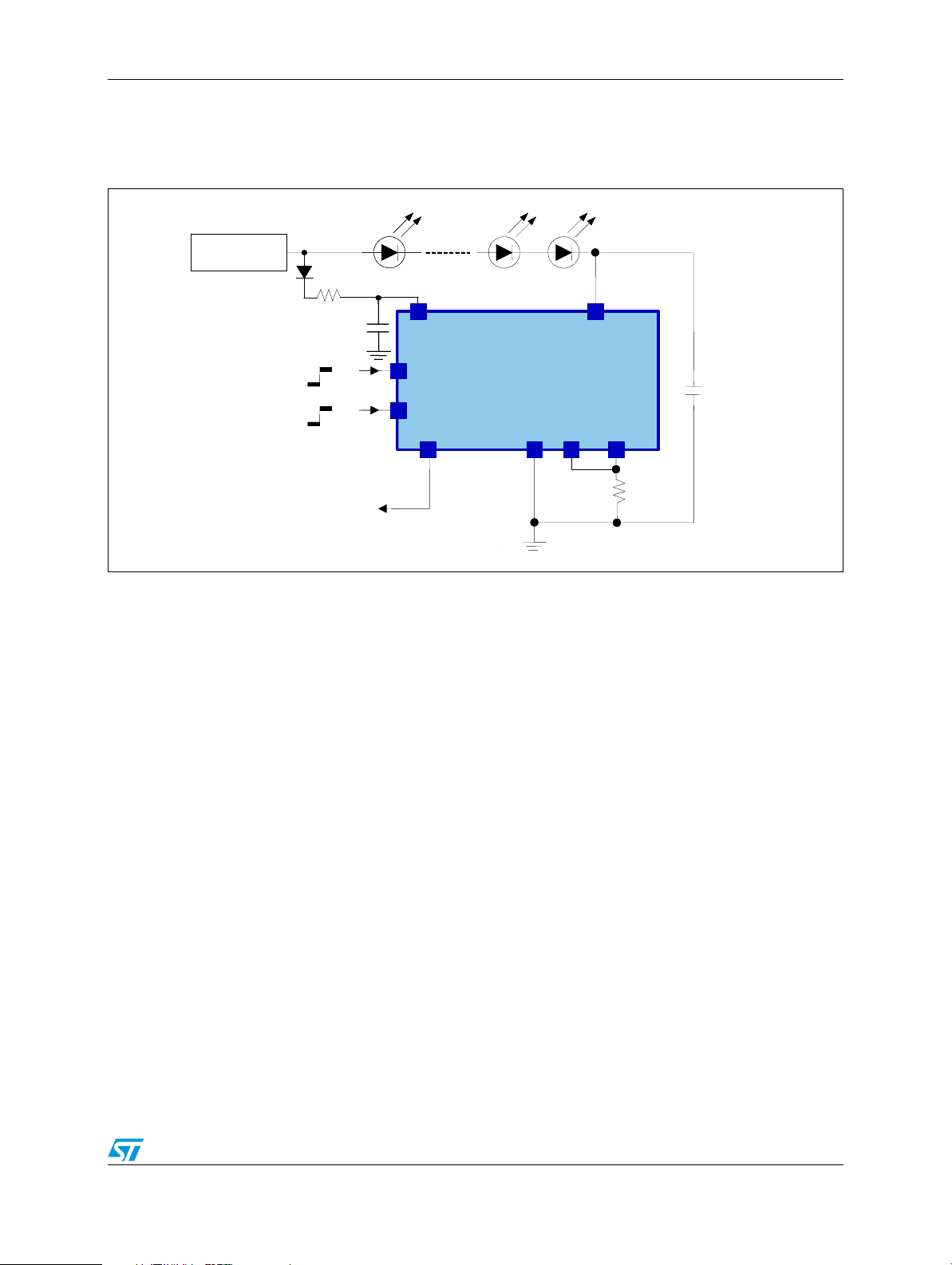
1 Application diagram
Figure 1. Typical application diagram for 2 A LED current
V
V
IN
IN
4.5V up to 40V
4.5V up to 40V
R
100 ohm
R
100 ohm
IN
IN
C
C
BYP
0.1µF
0.1µF
ON
ON
OFF
OFF
ON
ON
OFF
OFF
Load disconnection
Load disconnection
(Open Drain output)
(Open Drain output)
BYP
V
V
CC
CC
PWM
PWM
EN
EN
DISC
DISC
STCS2
STCS2
GND
GND
DRAIN
DRAIN
FB
FB
SOURCE
SOURCE
R
R
0.05 ohm
0.05 ohm
C
C
DRAIN
DRAIN
0.47µF
0.47µF
FB
FB
3/16
Pin configuration STCS2
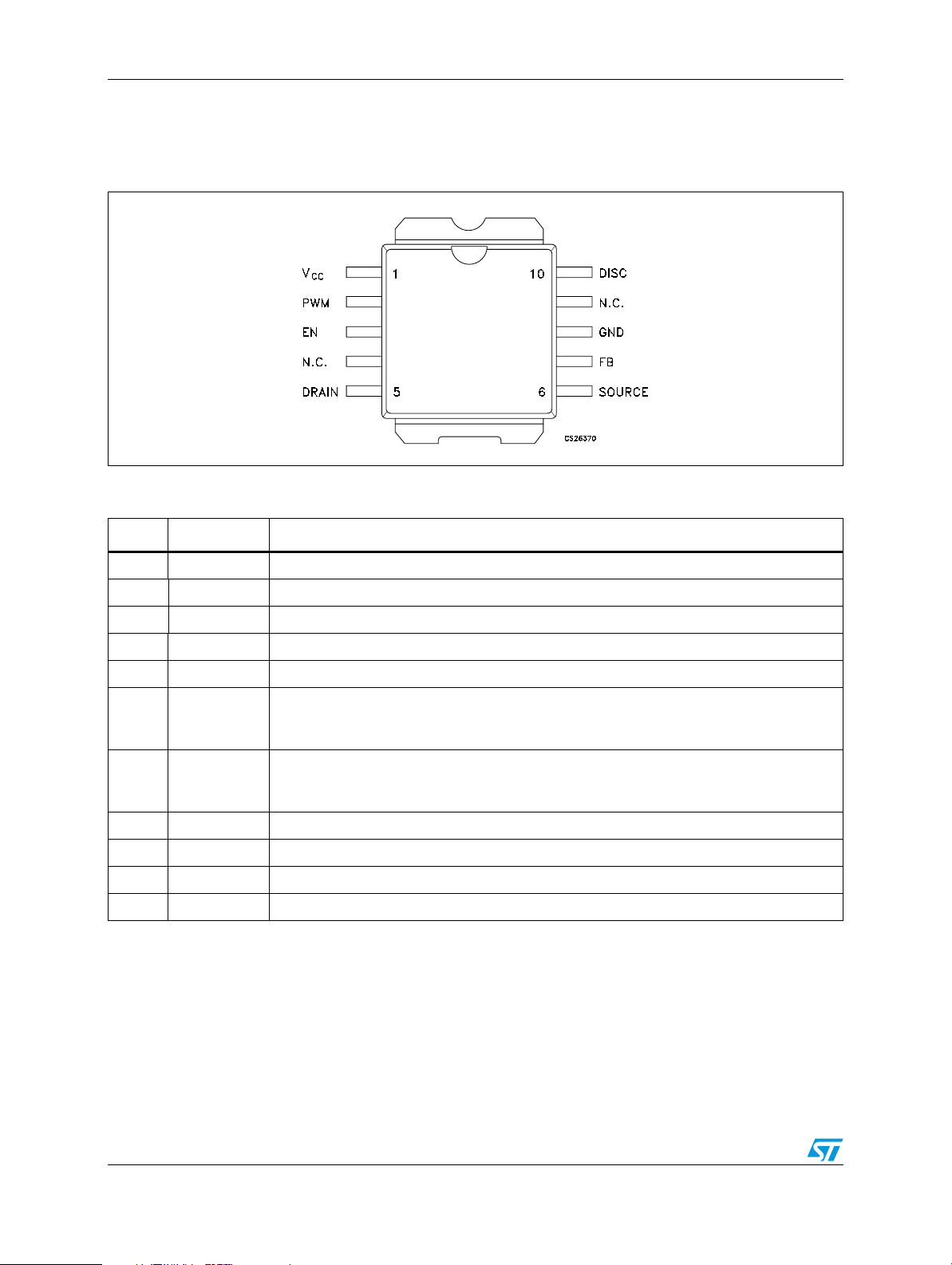
2 Pin configuration
Figure 2. Pin connections (top view)
Table 2. Pin description
Pin n° Symbol Note
1V
2 PWM PWM dimming input
3ENShutdown
4 N.C. Not connected
5 DRAIN Internal N-MOSFET drain
6 SOURCE
7FB
8 GND Ground
9 N.C. In order to guarantee the device works properly it is mandatory to leave this pin floating
10 DISC Load disconnection flag (open drain)
CC
Exp-pad Internally connected to ground
Supply voltage
Internal N-MOSFET SOURCE. Reference voltage is 100 mV. An external resistor
between SOURCE and GND pins sets different current levels for different application
needs
Feedback input. The control loop regulates the current in such a way that the average
voltage at the FB input is 100 mV (nominal). The cathode of the LED and a resistor to
ground to set the LED current should be connected at this point
4/16
STCS2 Maximum ratings
3 Maximum ratings
Table 3. Absolute maximum ratings
Symbol Parameter Value Unit
V
CC
DC supply voltage -0.3 to +45
V
DRAIN Drain pin -0.3 to +45
SOURCE Source pin -0.3 to + 3.3 V
PWM, EN, DISC Logic pins -0.3 to + V
+ 0.3 V
CC
FB Configuration pins -0.3 to + 3.3 V
ESD Human body model (all pins) ±2 kV
(1)
T
J
T
STG
1. TJ is calculated from the ambient temperature TA and the power dissipation PD according the following formula:
T
= TA + (PD x R
J
Junction temperature -40 to 150 °C
Storage temperature range -55 to 150 °C
). See Figure 12 for details of max power dissipation for ambient temperatures higher than 25°C.
thJA
Note: Absolute maximum ratings are those values beyond which damage to the device may occur.
Functional operation under these conditions is not implied.
Table 4. Thermal data
Symbol Parameter PowerSO-10 Unit
R
thJC
R
thJA
R
thJA
R
thJA
1. FR4 with using the recommended pad-layout
2. FR4 with heat sink on board (6 cm
3. FR4 with copper-filled through holes and external heat sink applied.
Thermal resistance junction-case 2 °C/W
Thermal resistance junction-ambient
Thermal resistance junction-ambient
Thermal resistance junction-ambient
2
).
(1)
(2)
(3)
50 °C/W
35 °C/W
12 °C/W
5/16
 Loading...