

ST STCS1 User Manual

Features
■ Up to 40 V input voltage
■ Less than 0.5 V voltage overhead
■ Up to 1.5 A output current
■ PWM dimming pin
■ Shutdown pin
■ LED disconnection diagnostic
Applications
STCS1
1.5 A max constant current LED driver
DFN8 (3x3 mm)
PowerSO-8
■ Supplying LEDs with constant current for
varying input voltages
■ Low voltage lighting
■ Small appliance LED lighting
■ Car LED lights
Description
The STCS1 is a BiCMOS constant current source
designed to provide a precise constant current
starting from a varying input voltage source. The
main target is to replace discrete components
solution for driving LEDs in low voltage
applications such as 5 V, 12 V or 24 V giving
benefits in terms of precision, integration and
reliability.
The current is set with external resistor up to 1.5
A with a ± 10 % precision; a dedicated pin allows
implementing PWM dimming.
An open-drain pin output provides information on
load disconnection condition.
Table 1. Device summary
Order codes Packages Packaging
STCS1PUR DFN8 (3 x 3 mm) 3000 parts per reel
STCS1PHR PowerSO-8 2500 parts per reel
July 2008 Rev 8 1/17
www.st.com
17

Contents STCS1
Contents
1 Application diagram . . . . . . . . . . . . . . . . . . . . . . . . . . . . . . . . . . . . . . . . . 3
2 Pin configuration . . . . . . . . . . . . . . . . . . . . . . . . . . . . . . . . . . . . . . . . . . . 4
3 Maximum ratings . . . . . . . . . . . . . . . . . . . . . . . . . . . . . . . . . . . . . . . . . . . . 5
4 Electrical characteristics . . . . . . . . . . . . . . . . . . . . . . . . . . . . . . . . . . . . . 6
5 Timing . . . . . . . . . . . . . . . . . . . . . . . . . . . . . . . . . . . . . . . . . . . . . . . . . . . . . 7
6 Typical performance characteristics . . . . . . . . . . . . . . . . . . . . . . . . . . . . 8
7 Detail description . . . . . . . . . . . . . . . . . . . . . . . . . . . . . . . . . . . . . . . . . . . 9
7.1 Current setting . . . . . . . . . . . . . . . . . . . . . . . . . . . . . . . . . . . . . . . . . . . . . . 9
7.2 Enable . . . . . . . . . . . . . . . . . . . . . . . . . . . . . . . . . . . . . . . . . . . . . . . . . . . . 9
7.3 PWM dimming . . . . . . . . . . . . . . . . . . . . . . . . . . . . . . . . . . . . . . . . . . . . . . 9
7.4 Diagnostic . . . . . . . . . . . . . . . . . . . . . . . . . . . . . . . . . . . . . . . . . . . . . . . . . . 9
8 Application information . . . . . . . . . . . . . . . . . . . . . . . . . . . . . . . . . . . . . 10
8.1 Reverse polarity protection . . . . . . . . . . . . . . . . . . . . . . . . . . . . . . . . . . . . 10
8.2 Thermal considerations . . . . . . . . . . . . . . . . . . . . . . . . . . . . . . . . . . . . . . 10
9 Package mechanical data . . . . . . . . . . . . . . . . . . . . . . . . . . . . . . . . . . . . 12
10 Revision history . . . . . . . . . . . . . . . . . . . . . . . . . . . . . . . . . . . . . . . . . . . 16
2/17
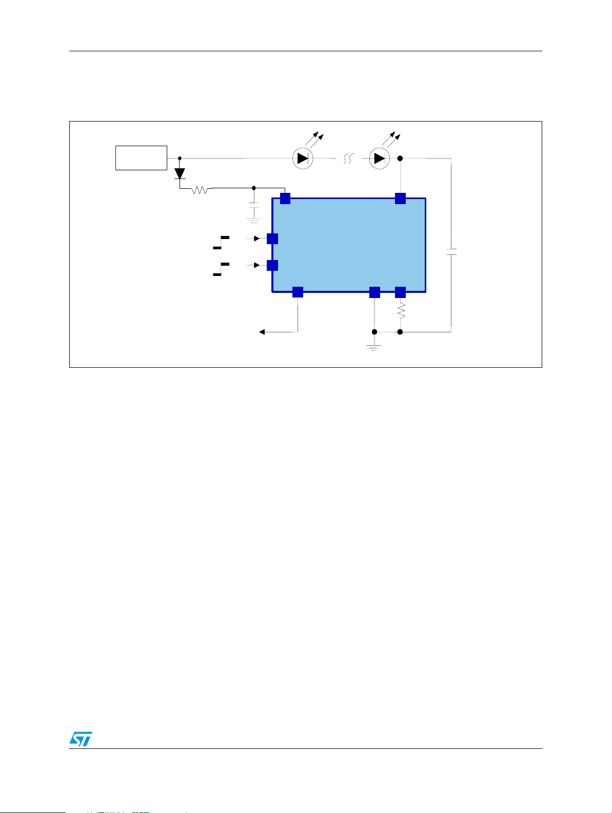
STCS1 Application diagram
1 Application diagram
Figure 1. Typical application diagram for 0.5 A LED current
V
V
IN
IN
4.5V to 40V
4.5V to 40V
BAT46ZFILM
BAT46ZFILM
RIN100 ohm
RIN100 ohm
OFF
OFF
OFF
OFF
C
C
BYP
BYP
0.1µF
0.1µF
ON
ON
ON
ON
Load disconnection
Load disconnection
(Open Drain output)
(Open Drain output)
V
V
PWM
PWM
EN
EN
CC
CC
DISC
DISC
STCS1
STCS1
GND
GND
DRAIN
DRAIN
FB
FB
R
R
FB
FB
0.2 ohm
0.2 ohm
C
C
DRAIN
DRAIN
0.47µF
0.47µF
3/17

Pin configuration STCS1
2 Pin configuration
Figure 2. Pin connections (top view)
DFN8
PowerSO-8
Table 2. Pin description
Pin n° Symbol Note
1V
2 PWM PWM dimming input
3 EN Shutdown pin
4 DRAIN Internal N-MOSFET drain
5FB
6 GND Ground
7 N.C. In order to guarantee the device works properly it is mandatory to leave this pin floating
8 DISC Load disconnection flag (open drain)
CC
Exp-pad Internally connected to ground
Supply voltage
Feedback input. The control loop regulates the current in such a way that the average
voltage at the FB input is 100 mV (nominal). The cathode of the LED and a resistor to
ground to set the LED current should be connected at this point
4/17

STCS1 Maximum ratings
3 Maximum ratings
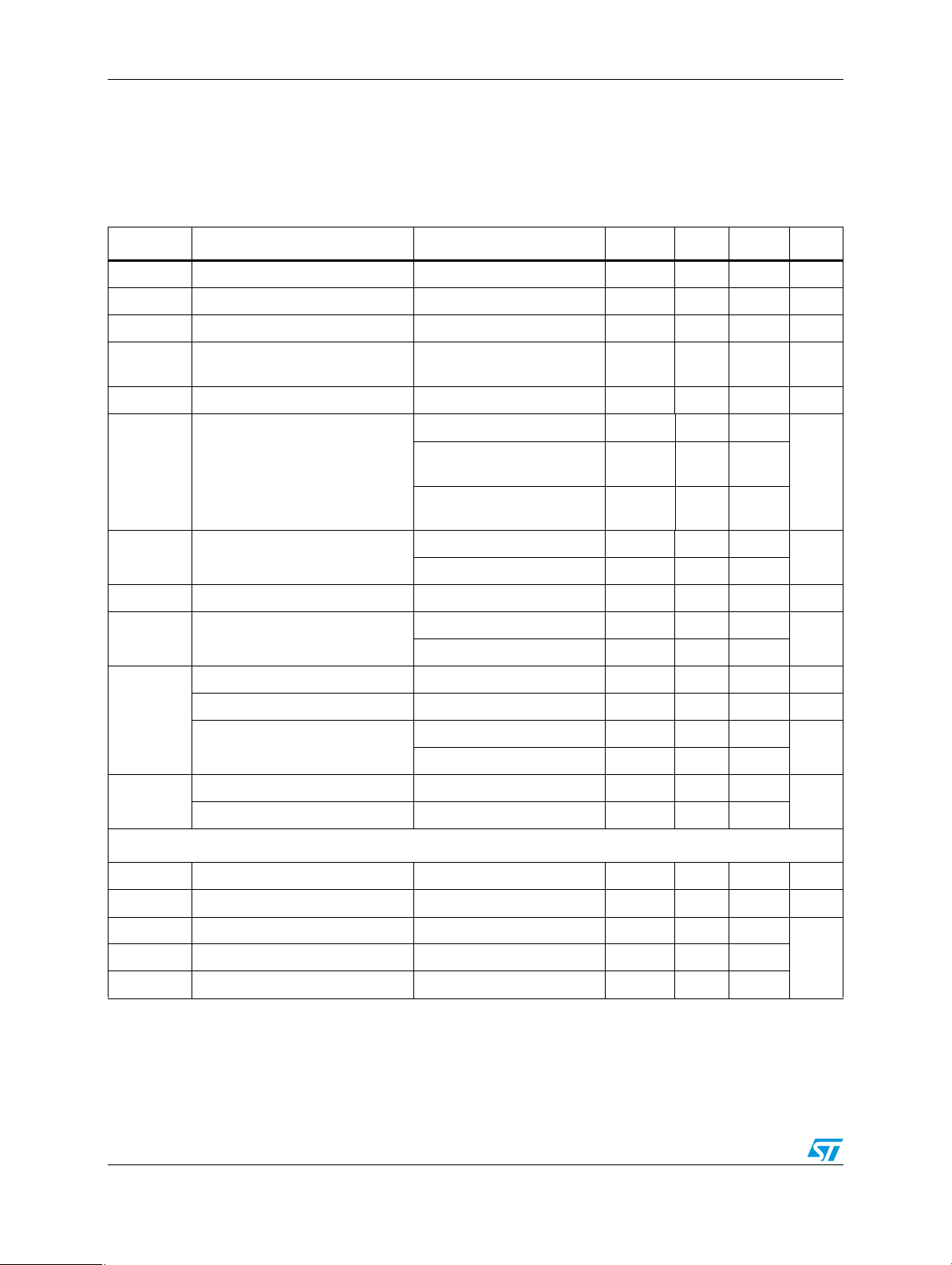
Table 3. Absolute maximum ratings
Symbol Parameter Value Unit
V
CC
DC supply voltage -0.3 to +45
V
DRAIN Drain pin -0.3 to +45
PWM, EN, DISC Logic pins -0.3 to + V
+ 0.3 V
CC
FB Configuration pins -0.3 to + 3.3 V
ESD Human body model (all pins) ±2 kV
(1)
T
J
T
STG
1. TJ is calculated from the ambient temperature TA and the power dissipation PD according the following formula:
= TA + (PD x R
T
J
than 25°C.
Junction temperature -40 to 150 °C
Storage temperature range -55 to 150 °C
). See Figure 12 and Figure 13 for details of max power dissipation for ambient temperatures higher
thJA
Note: Absolute maximum ratings are those values beyond which damage to the device may occur.
Functional operation under these conditions is not implied.
Table 4. Thermal data
Symbol Parameter DFN8 PowerSO-8 Unit
R
thJC
R
thJA
1. This value is referred to four-layer PCB, JEDEC standard test board.
2. With two sides, two planes PCB following EIA/JEDEC JESD51-7 standard.
Thermal resistance junction-case 10 12 °C/W
Thermal resistance junction-ambient 37.6
(1)
45
(2)
°C/W
5/17
Electrical characteristics STCS1
4 Electrical characteristics
Table 5. Electrical characteristics
(V
= 12 V; IO = 100 mA; TJ = -40 °C to 125 °C; V
CC
nF typical values are at T
= 25 °C, unless otherwise specified)
A
Symbol Parameter Test conditions Min. Typ. Max. Unit
DRAIN
= 1 V; C
DRAIN
= 1 µF; C
BYP
= 100
V
CC
I
O
V
FB
I
CC
V
DROP
LEAK
DRAIN
T
D
DISC
Thermal
Protection
Supply voltage range 4.5 40 V
Output current range 1 1500 mA
Output current R
Regulation (percentage with
respect to V
CC
=12V)
= 0.2 Ω 500 mA
FB
V
= 4.5 to 40 V,
CC
IO = 100 mA; V
DRAIN
= 1 V
-1 +1 %
Feedback voltage IO = 0 to 1.5A 90 100 110 mV
On Mode 450 750
Quiescent current (Measured on
VCC pin)
Shutdown Mode;
= 5 to 12V
V
CC
Shutdown Mode;
V
= 12 to 40V
CC
I
= 100 mA 0.12 0.16
Dropout voltage (V
DRAIN
to GND)
O
= 1.5 A 0.58 0.9
I
O
Drain leakage current Shutdown; V
rising, V
V
Delay on PWM signal
(see Figure 3)
Low level voltage I
Leakage current V
Load disconnection threshold
DRAIN
-GND)
(V
PWM
falling, V
V
PWM
= 5 mA 0.2 0.5 V
SINK
= 5 V 1 µA
DISC
DISC Turn-ON 75
DISC Turn-OFF 110
= 40 V 10 µA
DRAIN
= 12 V 3
CC
= 12 V 1.2
CC
1
µA
3
V
µs
mV
Shutdown temperature 155
°C
Hysteresis 25
Logic inputs (PWM and EN)
V
V
Input low level 0.4 V
L
Input high level 1.2 V
H
EN, PWM leakage current V
PWM input leakage current V
= 5 V; V
EN
= 40 V 60
EN
= 40 V 120
PWM
= 5 V 2
PWM
µAEN input leakage current V
Note: All devices 100 % production tested at TA = 25 °C. Limits over the operating temperature
range are guaranteed by design.
6/17
 Loading...