

High power white LED SuperCap™ driver with I²C interface
Features
■ Buck-boost converter with 1.5 A peak current
limiting and synchronous rectification
■ Burst mode operation when output is charged
■ Input voltage range 2.5 V to 5.5 V
■ Programmable output charging voltage up to
5.5 V
■ Full I²C control
■ Operation modes:
– Shutdown mode
– Monitoring mode with NTC and SuperCap
monitoring
– Idle mode
–Flash mode
– Torch mode: up to 320 mA
■ Controlled LED current in all modes
■ Soft and hard triggering of Flash, Torch and
Picture light modes
■ Torch dimming in 12 exponential steps
■ Flash dimming in 8 steps
■ Active balancing of SuperCap voltage
■ SuperCap status flag
■ Internally or externally timed flash operation
■ Digitally programmable safety timeout in Flash
mode
■ Torch mode safety timeout
■ LED overtemperature detection and protection
with external NTC resistor
■ Shorted LED failure detection and protection
■ Chip overtemperature detection and protection
STCF04
Datasheet − production data
TFBGA25 (3 x 3 mm)
Applications
■ Cell phones and smartphones
■ Camera flashes/strobe
■ PDAs and digital still cameras
Description
The STCF04 is a dedicated and space optimized
high efficiency solution for driving a flash LED
module in cameras, phones, PDAs and other
handheld devices using the SuperCap
technology. It is based on a DC-DC buck-boost
converter, which ensures a proper and efficient
charging control and monitoring of the SuperCap
in the whole battery voltage range. The output
current control ensures a good current regulation
over the forward voltage spread characteristics of
the flash LEDs in Torch and Flash mode
operation. The SuperCap charging current is
limited to a defined value which avoids overload of
the battery. The SuperCap discharge current
flows through the LEDs and the external
MOSFET which must be chosen according to the
desired flash current.
Table 1. Device summary
Order code Package Packaging
STCF04TBR TFBGA25 (3 x 3 mm) 3000 parts per reel
May 2012 Doc ID 022927 Rev 2 1/43
This is information on a product in full production.
www.st.com
43

Contents STCF04
Contents
1 Description (continued) . . . . . . . . . . . . . . . . . . . . . . . . . . . . . . . . . . . . . . 5
2 Diagram . . . . . . . . . . . . . . . . . . . . . . . . . . . . . . . . . . . . . . . . . . . . . . . . . . . 6
3 Pin configuration . . . . . . . . . . . . . . . . . . . . . . . . . . . . . . . . . . . . . . . . . . . . 7
4 Maximum ratings . . . . . . . . . . . . . . . . . . . . . . . . . . . . . . . . . . . . . . . . . . . 8
5 Application . . . . . . . . . . . . . . . . . . . . . . . . . . . . . . . . . . . . . . . . . . . . . . . . . 9
6 Electrical characteristics . . . . . . . . . . . . . . . . . . . . . . . . . . . . . . . . . . . . 11
7 Introduction . . . . . . . . . . . . . . . . . . . . . . . . . . . . . . . . . . . . . . . . . . . . . . . 14
8 Detailed description . . . . . . . . . . . . . . . . . . . . . . . . . . . . . . . . . . . . . . . . 15
8.1 Logic pins . . . . . . . . . . . . . . . . . . . . . . . . . . . . . . . . . . . . . . . . . . . . . . . . . 15
8.1.1 SCL, SDA pins . . . . . . . . . . . . . . . . . . . . . . . . . . . . . . . . . . . . . . . . . . . . 15
8.1.2 FLASH pin . . . . . . . . . . . . . . . . . . . . . . . . . . . . . . . . . . . . . . . . . . . . . . . 15
8.1.3 TORCH pin . . . . . . . . . . . . . . . . . . . . . . . . . . . . . . . . . . . . . . . . . . . . . . 15
8.1.4 RESET pin . . . . . . . . . . . . . . . . . . . . . . . . . . . . . . . . . . . . . . . . . . . . . . . 15
8.1.5 ATN pin . . . . . . . . . . . . . . . . . . . . . . . . . . . . . . . . . . . . . . . . . . . . . . . . . 15
8.1.6 ADD pin . . . . . . . . . . . . . . . . . . . . . . . . . . . . . . . . . . . . . . . . . . . . . . . . . 15
8.1.7 READY pin . . . . . . . . . . . . . . . . . . . . . . . . . . . . . . . . . . . . . . . . . . . . . . . 16
8.1.8 Data validity . . . . . . . . . . . . . . . . . . . . . . . . . . . . . . . . . . . . . . . . . . . . . . 17
8.1.9 START and STOP conditions . . . . . . . . . . . . . . . . . . . . . . . . . . . . . . . . . 17
8.1.10 Byte format . . . . . . . . . . . . . . . . . . . . . . . . . . . . . . . . . . . . . . . . . . . . . . 18
8.1.11 Acknowledge . . . . . . . . . . . . . . . . . . . . . . . . . . . . . . . . . . . . . . . . . . . . . 18
8.1.12 Interface protocol . . . . . . . . . . . . . . . . . . . . . . . . . . . . . . . . . . . . . . . . . . 19
8.1.13 Writing to a single register . . . . . . . . . . . . . . . . . . . . . . . . . . . . . . . . . . . 19
8.1.14 Writing to multiple registers with incremental addressing . . . . . . . . . . . 20
8.1.15 Reading from a single register . . . . . . . . . . . . . . . . . . . . . . . . . . . . . . . . 20
8.1.16 Reading from multiple registers with incremental addressing . . . . . . . . 21
9 Description of the internal registers . . . . . . . . . . . . . . . . . . . . . . . . . . . 22
9.1 Commands (CMD_REG) 00(hex) . . . . . . . . . . . . . . . . . . . . . . . . . . . . . . 22
2/43 Doc ID 022927 Rev 2

STCF04 Contents
9.1.1 PWR_ON . . . . . . . . . . . . . . . . . . . . . . . . . . . . . . . . . . . . . . . . . . . . . . . . 22
9.1.2 FLASH_ON . . . . . . . . . . . . . . . . . . . . . . . . . . . . . . . . . . . . . . . . . . . . . . 22
9.1.3 TCH_ON . . . . . . . . . . . . . . . . . . . . . . . . . . . . . . . . . . . . . . . . . . . . . . . . 23
9.1.4 NTC_ON . . . . . . . . . . . . . . . . . . . . . . . . . . . . . . . . . . . . . . . . . . . . . . . . 23
9.1.5 TCHV_H . . . . . . . . . . . . . . . . . . . . . . . . . . . . . . . . . . . . . . . . . . . . . . . . 23
9.1.6 CHRG . . . . . . . . . . . . . . . . . . . . . . . . . . . . . . . . . . . . . . . . . . . . . . . . . . 23
9.1.7 MONTR . . . . . . . . . . . . . . . . . . . . . . . . . . . . . . . . . . . . . . . . . . . . . . . . . 23
9.2 Flash register (FL_REG) 01(hex) . . . . . . . . . . . . . . . . . . . . . . . . . . . . . . . 23
9.3 AUX LED (AUX_REG) 02(hex) . . . . . . . . . . . . . . . . . . . . . . . . . . . . . . . . . 24
9.4 Status (STAT_REG) 03(hex) . . . . . . . . . . . . . . . . . . . . . . . . . . . . . . . . . . 25
9.5 Feature (FTR_REG) 04(hex) . . . . . . . . . . . . . . . . . . . . . . . . . . . . . . . . . . 26
9.6 Torch register (TRCH_REG) 05(hex) . . . . . . . . . . . . . . . . . . . . . . . . . . . . 27
10 Theory of operation . . . . . . . . . . . . . . . . . . . . . . . . . . . . . . . . . . . . . . . . 28
10.1 The state machine diagram . . . . . . . . . . . . . . . . . . . . . . . . . . . . . . . . . . . 28
10.2 Power-ON reset . . . . . . . . . . . . . . . . . . . . . . . . . . . . . . . . . . . . . . . . . . . . 29
10.2.1 RESET pin function . . . . . . . . . . . . . . . . . . . . . . . . . . . . . . . . . . . . . . . . 29
10.3 Shutdown mode and NTC mode . . . . . . . . . . . . . . . . . . . . . . . . . . . . . . . 29
10.4 Monitoring mode . . . . . . . . . . . . . . . . . . . . . . . . . . . . . . . . . . . . . . . . . . . 29
10.5 Idle mode . . . . . . . . . . . . . . . . . . . . . . . . . . . . . . . . . . . . . . . . . . . . . . . . . 30
10.6 AUX LED . . . . . . . . . . . . . . . . . . . . . . . . . . . . . . . . . . . . . . . . . . . . . . . . . 30
10.7 Single or multiple flash using external (microprocessor) temporization . . 30
10.8 External (microprocessor) temporization using the FLASH_ON bit . . . . . 31
10.9 Single flash using internal temporization . . . . . . . . . . . . . . . . . . . . . . . . . 31
10.10 Light sensor feature . . . . . . . . . . . . . . . . . . . . . . . . . . . . . . . . . . . . . . . . . 31
11 Typical performance characteristics . . . . . . . . . . . . . . . . . . . . . . . . . . . 32
12 Package mechanical data . . . . . . . . . . . . . . . . . . . . . . . . . . . . . . . . . . . . 38
13 Revision history . . . . . . . . . . . . . . . . . . . . . . . . . . . . . . . . . . . . . . . . . . . 42
Doc ID 022927 Rev 2 3/43

List of tables STCF04
List of tables
Table 1. Device summary . . . . . . . . . . . . . . . . . . . . . . . . . . . . . . . . . . . . . . . . . . . . . . . . . . . . . . . . . . 1
Table 2. Pin description . . . . . . . . . . . . . . . . . . . . . . . . . . . . . . . . . . . . . . . . . . . . . . . . . . . . . . . . . . . 8
Table 3. Absolute maximum ratings . . . . . . . . . . . . . . . . . . . . . . . . . . . . . . . . . . . . . . . . . . . . . . . . . . 9
Table 4. Thermal data. . . . . . . . . . . . . . . . . . . . . . . . . . . . . . . . . . . . . . . . . . . . . . . . . . . . . . . . . . . . . 9
Table 5. List of external components . . . . . . . . . . . . . . . . . . . . . . . . . . . . . . . . . . . . . . . . . . . . . . . . 11
Table 6. Electrical characteristics . . . . . . . . . . . . . . . . . . . . . . . . . . . . . . . . . . . . . . . . . . . . . . . . . . . 12
Table 7. I²C address table . . . . . . . . . . . . . . . . . . . . . . . . . . . . . . . . . . . . . . . . . . . . . . . . . . . . . . . . 17
Table 8. Interface protocol . . . . . . . . . . . . . . . . . . . . . . . . . . . . . . . . . . . . . . . . . . . . . . . . . . . . . . . . 20
Table 9. I²C register mapping . . . . . . . . . . . . . . . . . . . . . . . . . . . . . . . . . . . . . . . . . . . . . . . . . . . . . . 23
Table 10. Command register . . . . . . . . . . . . . . . . . . . . . . . . . . . . . . . . . . . . . . . . . . . . . . . . . . . . . . . 23
Table 11. Flash register . . . . . . . . . . . . . . . . . . . . . . . . . . . . . . . . . . . . . . . . . . . . . . . . . . . . . . . . . . . 24
Table 12. Flash mode dimming registers settings (EXT_REG = 0) . . . . . . . . . . . . . . . . . . . . . . . . . . 24
Table 13. Flash time dimming register settings . . . . . . . . . . . . . . . . . . . . . . . . . . . . . . . . . . . . . . . . . 25
Table 14. AUX LED register . . . . . . . . . . . . . . . . . . . . . . . . . . . . . . . . . . . . . . . . . . . . . . . . . . . . . . . . 25
Table 15. Auxiliary LED dimming table . . . . . . . . . . . . . . . . . . . . . . . . . . . . . . . . . . . . . . . . . . . . . . . . 25
Table 16. Auxiliary LED timing table . . . . . . . . . . . . . . . . . . . . . . . . . . . . . . . . . . . . . . . . . . . . . . . . . . 26
Table 17. Status register. . . . . . . . . . . . . . . . . . . . . . . . . . . . . . . . . . . . . . . . . . . . . . . . . . . . . . . . . . . 26
Table 18. Status register details . . . . . . . . . . . . . . . . . . . . . . . . . . . . . . . . . . . . . . . . . . . . . . . . . . . . . 27
Table 19. Feature register . . . . . . . . . . . . . . . . . . . . . . . . . . . . . . . . . . . . . . . . . . . . . . . . . . . . . . . . . 27
Table 20. Light sensor reference dimming register settings . . . . . . . . . . . . . . . . . . . . . . . . . . . . . . . . 27
Table 21. DC-DC converter output voltages (V
Table 22. DC-DC converter coil peak current limit values . . . . . . . . . . . . . . . . . . . . . . . . . . . . . . . . . 28
Table 23. Torch register . . . . . . . . . . . . . . . . . . . . . . . . . . . . . . . . . . . . . . . . . . . . . . . . . . . . . . . . . . . 28
Table 24. Torch mode dimming registers settings . . . . . . . . . . . . . . . . . . . . . . . . . . . . . . . . . . . . . . . 28
Table 25. The safety timeout for Torch mode . . . . . . . . . . . . . . . . . . . . . . . . . . . . . . . . . . . . . . . . . . . 28
Table 26. Document revision history . . . . . . . . . . . . . . . . . . . . . . . . . . . . . . . . . . . . . . . . . . . . . . . . . 42
) . . . . . . . . . . . . . . . . . . . . . . . . . . . . . . . . . . . . . . 27
OUT
4/43 Doc ID 022927 Rev 2

STCF04 List of figures
List of figures
Figure 1. Block diagram . . . . . . . . . . . . . . . . . . . . . . . . . . . . . . . . . . . . . . . . . . . . . . . . . . . . . . . . . . . . 7
Figure 2. Pin connection (top view) . . . . . . . . . . . . . . . . . . . . . . . . . . . . . . . . . . . . . . . . . . . . . . . . . . . 8
Figure 3. Application schematic . . . . . . . . . . . . . . . . . . . . . . . . . . . . . . . . . . . . . . . . . . . . . . . . . . . . . 10
Figure 4. Behavior of the READY pin in different modes . . . . . . . . . . . . . . . . . . . . . . . . . . . . . . . . . . 17
Figure 5. Data validity on the I²C bus. . . . . . . . . . . . . . . . . . . . . . . . . . . . . . . . . . . . . . . . . . . . . . . . . 18
Figure 6. Timing diagram on I²C bus . . . . . . . . . . . . . . . . . . . . . . . . . . . . . . . . . . . . . . . . . . . . . . . . . 18
Figure 7. Bit transfer . . . . . . . . . . . . . . . . . . . . . . . . . . . . . . . . . . . . . . . . . . . . . . . . . . . . . . . . . . . . . 19
Figure 8. Acknowledge on I²C bus . . . . . . . . . . . . . . . . . . . . . . . . . . . . . . . . . . . . . . . . . . . . . . . . . . . 19
Figure 9. Writing to a single register . . . . . . . . . . . . . . . . . . . . . . . . . . . . . . . . . . . . . . . . . . . . . . . . . 20
Figure 10. Writing to multiple registers with incremental addressing . . . . . . . . . . . . . . . . . . . . . . . . . . 21
Figure 11. Reading from a single register . . . . . . . . . . . . . . . . . . . . . . . . . . . . . . . . . . . . . . . . . . . . . . 21
Figure 12. Reading from multiple registers . . . . . . . . . . . . . . . . . . . . . . . . . . . . . . . . . . . . . . . . . . . . . 22
Figure 13. State machine diagram of the STCF04 . . . . . . . . . . . . . . . . . . . . . . . . . . . . . . . . . . . . . . . 29
Figure 14. Reset timing . . . . . . . . . . . . . . . . . . . . . . . . . . . . . . . . . . . . . . . . . . . . . . . . . . . . . . . . . . . . 30
Figure 15. Flash current vs. input voltage . . . . . . . . . . . . . . . . . . . . . . . . . . . . . . . . . . . . . . . . . . . . . . 33
Figure 16. Torch current vs. input voltage . . . . . . . . . . . . . . . . . . . . . . . . . . . . . . . . . . . . . . . . . . . . . . 33
Figure 17. Aux LED current vs. input voltage . . . . . . . . . . . . . . . . . . . . . . . . . . . . . . . . . . . . . . . . . . . 34
Figure 18. Charging efficiency vs. V
Figure 19. Torch time - settings compared to real values . . . . . . . . . . . . . . . . . . . . . . . . . . . . . . . . . . 35
Figure 20. Torch current - settings compared to real values . . . . . . . . . . . . . . . . . . . . . . . . . . . . . . . . 35
Figure 21. Flash time - settings compared to real values . . . . . . . . . . . . . . . . . . . . . . . . . . . . . . . . . . 35
Figure 22. Flash current - settings compared to real values . . . . . . . . . . . . . . . . . . . . . . . . . . . . . . . . 36
Figure 23. Aux LED time - settings compared to real values. . . . . . . . . . . . . . . . . . . . . . . . . . . . . . . . 36
Figure 24. Aux LED current- settings compared to real values . . . . . . . . . . . . . . . . . . . . . . . . . . . . . . 36
Figure 25. Operation in Flash mode - single flash pulse . . . . . . . . . . . . . . . . . . . . . . . . . . . . . . . . . . . 37
Figure 26. Operation in Flash mode - multiple flash pulses. . . . . . . . . . . . . . . . . . . . . . . . . . . . . . . . . 37
Figure 27. Operation in Torch mode with TCHV_H bit = 0 . . . . . . . . . . . . . . . . . . . . . . . . . . . . . . . . . 38
Figure 28. Operation in Torch mode with TCHV_H bit = 1 . . . . . . . . . . . . . . . . . . . . . . . . . . . . . . . . . 38
voltage (VIN = 3.6 V) . . . . . . . . . . . . . . . . . . . . . . . . . . . . . . 34
OUT
Doc ID 022927 Rev 2 5/43

Description (continued) STCF04
1 Description (continued)
All the functions of the device are controlled through the I²C bus which reduces the number
of logic pins of the package and saves PCB tracks on the application board. Hard and softtriggering of flash and torch are both supported. The device includes many functions to
protect the chip and the power LEDs. These include a soft-start control, chip
overtemperature detection and protection, and shorted LED detection and protection. In
addition, a digital programmable timeout function protects the LEDs in case of a wrong
command issued by the microprocessor. An optional external NTC is supported to protect
the LEDs against overheating. It is possible to separately program the current intensity in
Flash and Torch mode through I²C. In order to guarantee the proper function of Flash mode,
the SuperCap voltage should be monitored by the microprocessor using the READY pin
feature. In case of insufficient power from the SuperCap, a warning is generated. The device
is packaged in BGA 3 x 3 mm with 1 mm height.
6/43 Doc ID 022927 Rev 2

STCF04 Diagram
2 Diagram
Figure 1. Block diagram
LSIN
NTC_ON
NTC_ON
LSIN
AUXLED
AUXLED
READY
READY
TORCH
TORCH
FLASH
FLASH
ATN
ATN
RESET
RESET
SCL
SCL
SDA
SDA
ADD
ADD
AUXLED
AUXLED
VBAT
VBAT
PREREG
PREREG
& BIAS
& BIAS
CONTROL
CONTROL
LOGIC
LOGIC
I²C
I²C
INTERF
INTERF
LSCON
LSCON
PVBAT
PVBAT
CONVERTER
CONVERTER
FLASH
FLASH
FLASH
FLASH
TRIGGERING
TRIGGERING
TRIGGERING
TRIGGERING
&CURRENT
&CURRENT
&CURRENT
&CURRENT
LIMITITING
LIMITITING
LIMITITING
LIMITITING
OSCILLATOR & TIME
OSCILLATOR & TIME
COUNTER
COUNTER
PROTECTIONS &
PROTECTIONS &
DIAGNOSTICS
DIAGNOSTICS
ON - CHIP
ON - CHIP
TEMP
TEMP
BUCK
BUCK
VLX1
VLX1
OVER -
OVER -
CURRENT
CURRENT
LED
LED
FAIL
FAIL
VLX2
VLX2
BOOST
BOOST
CONVERTER
CONVERTER
TORCH
TORCH
TORCH
TORCH
DIMMING
DIMMING
DIMMING
DIMMING
NTC_W
NTC_W
NTC_H
NTC_H
+
+
-
-
+
+
-
-
SUPERCAP
SUPERCAP
BALANCING &
BALANCING &
SUPERCAP
SUPERCAP
VOLTAGE
VOLTAGE
BALANCING &
BALANCING &
CONTROL
CONTROL
VOLTAGE
VOLTAGE
CONTROL
CONTROL
REF4
REF4
NTC_ON
NTC_ON
REF5
REF5
CURRENT
CURRENT
SENSING
SENSING
NTC
NTC
BIAS
BIAS
REF
REF
120 mV..1.2 V
120 mV..1.2 V
MX
MX
MX
MX
ENABLE/
ENABLE/
1.8 V REF
1.8 V REF
VOUT
VOUT
VMID
VMID
DRIVE
DRIVE
LED
LED
PGND
PGND
ISENS
ISENS
NTCRXPGND AGND
NTCRXPGND AGND
Doc ID 022927 Rev 2 7/43
Pin configuration STCF04
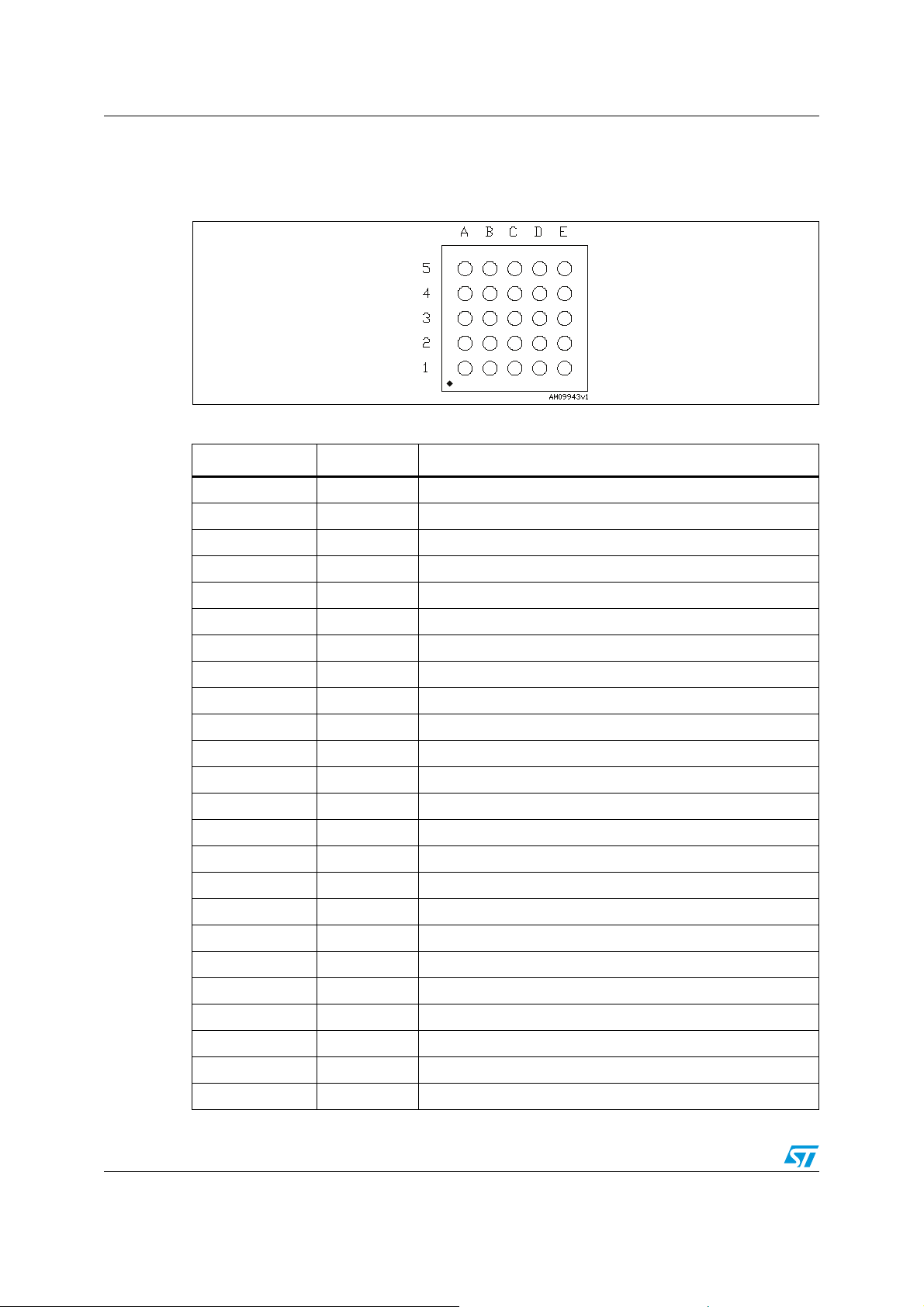
3 Pin configuration
Figure 2. Pin connection (top view)
Table 2. Pin description
Pin Symbol Description
A1 VLX1 Inductor connection 1
E1 VLX2 Inductor connection 2
D5 R
D1 VOUT SuperCap connection
C1 VMID SuperCap middle pin connection
E5 NTC NTC resistor connection
A3 READY SuperCap status flag pin
B3 SCL I²C clock signal
A4 FLASH Flash trigger input
E2 AGND Signal ground
B5 TORCH Torch trigger input
B4 RESET External reset input
D4 ISENS Flash regulator sensing connection
C3 ADD I²C address selection
E4 LED Diode module cathode connection
C4 ATN Attention (open drain output, active LOW)
B1 PVBAT Supply voltage
A5 SDA I²C data
E3 AUXLED Auxiliary red LED connection
B2 LSCON Light sensor capacitor connection
X
RX resistor connection
D3 VBAT Signal supply voltage
A2 LSIN Light sensor input
C5 DRIVE MOSFET driver output
C2, D2 PGND Power ground + die back connection
8/43 Doc ID 022927 Rev 2

STCF04 Maximum ratings
4 Maximum ratings
Table 3. Absolute maximum ratings
Symbol Parameter Value Unit
VBAT, PVBAT Signal supply voltage - 0.3 to 6 V
VLX Inductor connection - 0.3 to 6 V
VOUT SuperCap connection - 0.3 to 6 V
VDCDC DC-DC converter output - 0.3 to 6 V
VMID SuperCap middle pin connection - 0.3 to 6 V
AUXLED AUXLED connection - 0.3 to 6 V
LED LED connection - 0.3 to 6 V
SCL, SDA, ATN, ADD,
READY, TORCH,
FLASH, RESET
Logic pins - 0.3 to V
+ 0.3 V
BAT
PVBAT Power supply voltage - 0.3 to V
+ 0.3 V
BAT
DRIVE External MOSFET drive - 0.3 to 6 V
LSIN Light sensor input - 0.3 to 6 V
LSCON Light sensor capacitor connection - 0.3 to 6 V
R
X
Connection for reference resistor - 0.3 to 3 V
NTC Connection for LED temperature sensing - 0.3 to 3 V
ISENS Flash regulator sensing connection - 0.3 to 3 V
ESD Human body model ± 2kV
P
T
T
STG
TOT
OP
T
J
Continuous power dissipation (at TA=70 °C) 1 W
Operating junction temperature range - 40 to 85 °C
Junction temperature - 40 to 150 °C
Storage temperature range - 65 to 150 °C
Note: Absolute maximum ratings are those values beyond which damage to the device may occur.
Functional operation under these conditions is not implied.
Table 4. Thermal data
Symbol Parameter Value Unit
R
thJA
1. This parameter corresponds to the PCB board, 8 layers with 1 inch² of cooling area.
Thermal resistance junction-ambient
(1)
56 °C/W
Doc ID 022927 Rev 2 9/43
Application STCF04
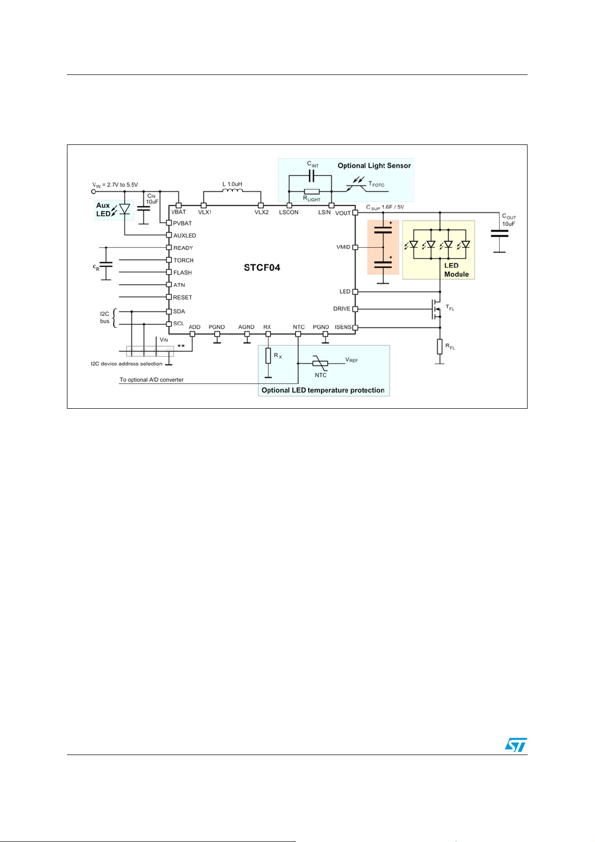
5 Application
Figure 3. Application schematic
Note: **: connect to VI, or GND or SDA or SCL to choose one of the 4 different I²C slave
addresses. Optional components to support auxiliary functions are highlighted with blue
rectangles.
Note: The anode of the AuxLED should be also connected to the V
OUT
.
10/43 Doc ID 022927 Rev 2

STCF04 Application
Table 5. List of external components
Component Manufacturer Part number Value Size
L
Murata LQM2HPN1R0MJC 1 µH / 1.5 A 2.5 x 2.0 x 1.1 mm
TDK VLS252012T-1R0N1R7 1 µH / 1.7 A 2.5 x 2.0 x 1.2 mm
CIN, COUT TDK C1608X5R0J106MT 10 µF / 6.3 V 0603
Rx Rohm MCR01MZPJ15K 15 kΩ 0402
NTC Murata NCP21WF104J03RA 100 kΩ 0805
Murata DME2W5R5K404M 400 mF / 5.5 V 20.5 x 18.5 x 3 mm
EDLC152344 550 mF / 5.5 V 44 x 23 x 1.5 mm
CSUP
TDK
EDLC272020 500 mF / 5.5 V 20 x 20 x 2.7 mm
CAP-xx GS 2 19F 1.6 F / 5 V 40 x 17 mm
LED MODULE Luxeon 4x LXCL-PWF4 White LED 0805
T
FL
R
FL
(1)
C
INT
R
* Tyco 0402
LIGHT
T
* Vishay TEMT6000 4 x 2 x 1 mm
FOTO
STMicroelectronics STL8NH3LL 8 A / 12 kΩ 3.3 x 3.3 x 0.9 mm
Tyco TL2BR01FTE 0R01 1206
TDK 10 µF / 6.3 V 0402
AUXLED Red LED 0603
C
R
1. Optional components for the auxiliary light sensor feature.
100 nF 0402
Note: The components listed above refer to a typical application. However, STCF04 operation is
not limited to the choice of these external components.
Doc ID 022927 Rev 2 11/43
Electrical characteristics STCF04
6 Electrical characteristics
TA = 25 °C, V
= 15 kΩ, V
R
X
Table 6. Electrical characteristics
= 3.6 V connected to V
IN
= 4.2 V/10 A. Unless otherwise specified, typical values are at 25 °C.
FLED
BAT
and P
VBAT
, C
IN
= 10 µF, C
= 1.6F/5 V L = 1 µH,
SUP
Symbol Parameter Test conditions Min. Typ. Max. Unit
V
V
PW_ON
RESET
IN
Operating input supply
voltage
Power-ON reset
threshold
2.5 5.5 V
VIN rising 2.3 V
Output current
Torch mode VIN=2.7 V to 5.5 V 15 320
Idle mode, VI or VO=3.3 V to 5.5 V 0 100
=2.7 V to 5.5 V, I
V
IN
= 10 mΩ
R
FL
V
=2.7 V to 5.5 V, IDC0=0 1.45
IN
=2.7 V to 5.5 V, IDC0=1 1.80
V
IN
LED
= 12 A
108 120 132 mV
V
ISENS
I
PEAK
adjustment range
I
I
O
TORCH
Auxiliary LED output
current adjustment
range I
AUXLED
Current sensing input
Switch peak current limit
Regulated voltage
range optimized for
V
=2.7 V to 5.5 V 4.5 5.5 V
IN
Flash mode
mA
A
V
OUT
I
MID
ΔI
Regulated voltage
range optimized for
Torch mode
V
tolerance
OUT
V
=2.7 V to 5.5 V
IN
Percentage with respect to
programmed voltage
V
+
FLED
0.25
-5 +5 %
V
Active balancing output VIN=2.7 V to 5.5 V -400 400 mA
Output current variation Torch mode I
O
Quiescent current in
Shutdown mode
Quiescent current in
Shutdown mode
I
Q
Quiescent current in
Monitoring mode
Quiescent current in Idle
mode
f
s
Switching frequency VIN=2.7 V 1.8 MHz
=2.7 to 5.5 V, NTC_ON=0 1
V
IN
VIN=2.7 to 5.5 V, NTC_ON=1 2
NTC_ON=0, SuperCap monitoring=1 45
NTC_ON, CHRG=0 1 mA
= 300 mA -10 10 %
LED
µA
12/43 Doc ID 022927 Rev 2

STCF04 Electrical characteristics
Table 6. Electrical characteristics (continued)
Symbol Parameter Test conditions Min. Typ. Max. Unit
Efficiency of the
converter
ν
Efficiency in Torch mode
operation
=3.7 V, VDC_0,1=1, IDC0=1 85
V
IN
=2.7 V to 4.2 V, IDC_0=1,
V
IN
TCHV_H=1 I
=2.7 V to 4.2 V, IDC_0=1,
V
IN
TCHV_H=0 I
V
SUPMAX
V
SUPHYST,
FLASH_ON=1
V
SUPMAX
V
SUPHYST,
FLASH_ON=1
V
SUPMAX
V
SUPHYST
V
SUPHYST
SuperCap regulated
voltage hysteresis
FLASH_ON=1
V
SUPMAX
V
SUPHYST
V
MONIREADY
OTP
OTHYST
SuperCap voltage ready
hysteresis
Overtemperature
protection
Overtemperature
hysteresis
PWR_ON=0, VDC_0 or/and VDC_1=1 0.2 V
=5.5 V 140 C
V
IN
=5.5 V 20 C
V
IN
V_NTCW NTC threshold warning Idle mode, I
V_NTCH NTC threshold hot Idle mode, I
VOL
Output logic signal level
low ATN, READY
I
ATN, READY
=320 mA
TORC H
=320 mA
TORC H
=5.5 V, V
SUPMIN
=5.5 V-
TCHV_H=1 or
=5.0 V, V
SUPMIN
=5.0 V-
TCHV_H=1 or
=4.5 V, V
SUPMIN
=4.5 V-
, TCHV_H=1 or
=4.2 V, V
SUPMIN
=4.2 V-
, TCHV_H=0
=2 mA max. 0.56 V
NTC
=2 mA max. 1.2 V
NTC
50
70
1.3
0.8
0.3
0.2
=+10 mA 0.3 V
%
V
I
OZ
V
IL
V
IH
I
LSCON
V
LSIN
V
DRIVE
T
ON
Output logic leakage
current ATN, READY
V
ATN, READY
=3.3 V 1 mA
Input logic signal level
SCL, SDA, TEST,
RESET, SCHRG,
=2.7 V to 5.5 V
V
IN
FLASH, TORCH, ADD
Input reset current VIN=2.7 V to 5.5 V, V
Analog input signal
range
MOSFET driver output
Reference voltage
range
LED current rise time
I
LED
=0 to I
LED
=max.
V
=2.7 V to 5.5 V 0.1 1.6 V
IN
Source: I
Sink: I
DRIVE
EXT_REG=1
= -8 mA 4.27 V
DRIVE
= +8 mA 1.05 V
(1)
Flash triggered by external trig 0.3 ms
Doc ID 022927 Rev 2 13/43
00.4
1.4 3.0
=1.6 V 10 mA
REF
0.12 1.2 V
V

Electrical characteristics STCF04
Table 6. Electrical characteristics (continued)
Symbol Parameter Test conditions Min. Typ. Max. Unit
T
RESMIN
T
LSCAPRES
Minimum RESET time VIN=2.7 V to 5.5 V 1 µs
Reset time of the light
sensor capacitor
200 µs
14/43 Doc ID 022927 Rev 2

STCF04 Introduction
7 Introduction
The STCF04 is a high efficiency buck-boost converter with input current limitation dedicated
to managing the power for Flash/Torch mode operations using the SuperCap technology
and to control the high current white LEDs in cell phone cameras and portable applications
in general.
The device operates in Free-running mode with a coil peak current limiter. It charges and
stores the energy on the SuperCap from a single cell lithium-Ion battery (2.5 V to 4.2 V). The
device contains an active balancer circuit able to regulate the middle pin of the SuperCap,
therefore guaranteeing the reliability of the SuperCap component. The device operation and
diagnostic are controlled by the I²C bus. Torch current is adjustable from 15 mA to 320 mA.
The maximum flash current is set by choosing the R
using a dedicated register. The device operates as a standalone flash SuperCap controller
able to drive one external MOSFET.
The device has two modes of managing the energy in the SuperCap during Torch mode
operation, both adjustable by I²C:
1. Torch mode 1: in this case the output current in Torch mode is regulated from V
which is set by VDC bits in the feature register (R4). This mode is optimized to give the
possibility of triggering the flash without any delay caused by a recharging of the
SuperCap.
2. Torch mode 2: in this case the output current in Torch mode is regulated from V
V
+ 0.25 V. This mode is optimized for maximum efficiency in Torch mode. The
FLED
SuperCap must be recharged after the end of Torch mode operation.
resistor and it can be adjusted by I²C
FL
OUT,
OUT
=
The device uses an external NTC resistor to sense the temperature of the white LEDs and
light sensor management to optimize the flash duration in Flash mode. These last two
functions are optional so they may not be needed in all applications, and, in such cases, the
relevant external components can be omitted. In Monitoring mode, when the voltage
Monitoring mode of the SuperCap is active, the device is working with low consumption.
When the READY pin goes HIGH, meaning that the SuperCap has been self-discharged,
the P should initiate a re-charge of the SuperCap, for example, by entering Charge mode.
Doc ID 022927 Rev 2 15/43

Detailed description STCF04
8 Detailed description
8.1 Logic pins
8.1.1 SCL, SDA pins
These are the standard CLOCK and DATA pins as defined in the I²C bus specifications.
External pull-ups are required according to I²C bus specifications.
8.1.2 FLASH pin
This input pin is internally AND-ed with the FLASH_ON bit to generate the internal signal
that activates the flash operation. This gives the user the possibility to accurately control the
flash duration using a dedicated pin, avoiding the I²C bus latencies (hard-triggering). Neither
internal pull-up nor pull-down is provided.
8.1.3 TORCH pin
This input pin is internally AND-ed with the TCH_ON bit to generate the internal signal that
activates the torch operation. Neither internal pull-up nor pull-down is provided.
8.1.4 RESET pin
This pin works as an external reset input. The microprocessor can use this pin to reset the
STCF04 at any time. Neither internal pull-up nor pull-down is provided. This pin is active
LOW.
8.1.5 ATN pin
This output pin (open drain, active LOW) is provided to better manage the information
transfer from the STCF04 to the microprocessor. Because of the limitations of a single
master I²C bus configuration, the microprocessor should regularly communicate with the
STCF04 to verify if certain operations have been completed, or to check diagnostic
information. Alternatively, the microprocessor can use the ATN pin to be advised that a new
data is available in the STAT_REG register, therefore avoiding continuous communication.
The information may then be read in the STAT_REG by a read operation via I²C which also
automatically resets the ATN pin to HIGH. The STAT_REG is also reset to 0. No internal
pull-up is provided.
8.1.6 ADD pin
This pin offers the opportunity of selecting one of the 4 possible I²C slave addresses.
Neither internal pull-up nor pull-down is provided. The pin must be connected to GND, VBAT,
SCL or SDA to select the desired I²C slave address (see
floating.
Ta bl e 7
). This pin cannot be left
16/43 Doc ID 022927 Rev 2

STCF04 Detailed description
Table 7. I²C address table
ADD pinA7A6A5A4A3A2A1A0
GND0110000R/W
VBAT0110001R/W
SDA0110010R/W
SCL0110011R/W
8.1.7 READY pin
This pin can be used to monitor the voltage on the SuperCap by the microprocessor. The
status of this pin has different meanings according to the current mode of operation of the
STCF04.
- Idle, Monitoring, Torch mode with TCHV_H=1:
The READY pin goes LOW when the SuperCap voltage reaches the threshold voltage set
by the V
voltage - 0.2 V of hysteresis. When READY is HIGH it means that it is necessary to recharge
the SuperCap in order to be able to make a flash.
- Torch mode with TCHV_H=0:
The READY pin goes LOW when the SuperCap reaches 4.2 V and is HIGH when the
SuperCap is below 4.2 V and Torch mode is not active.
register, otherwise the READY pin is HIGH when V
DC
SuperCap
goes below VDC
- FLASH:
The READY pin goes LOW as soon as the SuperCap voltage reaches the threshold voltage
set by the V
register. It stays LOW until the SuperCap voltage decreases below 4.2 V and
DC
Flash mode is not active. This feature allows the user to perform multiple flashes.
See
Figure 4
below for details.
Figure 4. Behavior of the READY pin in different modes
Doc ID 022927 Rev 2 17/43

Detailed description STCF04
Data transmission from the main microprocessor to the STCF04 and vice versa takes place
through the 2 I²C bus interface wires, consisting of the two lines SDA and SCL (pull-up
resistors to a positive supply voltage must be externally connected).
8.1.8 Data validity
As shown in
Figure 5
, the data on the SDA line must be stable during the high period of the
clock. The HIGH and LOW state of the data line can only change when the clock signal on
the SCL line is LOW.
Figure 5. Data validity on the I²C bus
8.1.9 START and STOP conditions
Both data and clock lines remain HIGH when the bus is not busy. As shown in
START condition is a HIGH to LOW transition of the SDA line while SCL is HIGH. The STOP
condition is a LOW to HIGH transition of the SDA line while SCL is HIGH. A STOP condition
must be sent before each START condition.
CS11340
Figure 6
, a
Figure 6. Timing diagram on I²C bus
18/43 Doc ID 022927 Rev 2

STCF04 Detailed description
8.1.10 Byte format
Every byte transferred to the SDA line must contain 8 bits. Each byte must be followed by an
acknowledge bit. The MSB is transferred first. One data bit is transferred during each clock
pulse. The data on the SDA line must remain stable during the HIGH period of the clock
pulse. Any change in the SDA line at this time is interpreted as a control signal.
Figure 7. Bit transfer
AM11867v 1
8.1.11 Acknowledge
The master (microprocessor) puts a resistive HIGH level on the SDA line during the
acknowledge clock pulse (see
pull down (LOW) the SDA line during the acknowledge clock pulse, so that the SDA line is
stable LOW during this clock pulse. The peripheral which has been addressed must
generate an acknowledge pulse after the reception of each byte, otherwise the SDA line
remains at the HIGH level during the ninth clock pulse duration. In this case, the master
transmitter can generate the STOP information in order to abort the transfer. The STCF04
does not generate the acknowledge bit if the V
Figure 8. Acknowledge on I²C bus
8.1.12 Interface protocol
Figure 8
). The peripheral (STCF04) that acknowledges must
supply is below 2.7 V.
I
The interface protocol is composed of (
- A START condition (START)
- A device address + R/W bit (read =1 / write =0)
- A register address byte
Doc ID 022927 Rev 2 19/43
Ta bl e 8
):

Detailed description STCF04
- A sequence of data n* (1 byte + acknowledge)
- A STOP condition (STOP)
The register address byte determines the first register in which the read or write operation
takes place. When the read or write operation is finished, the register address is
automatically incremented.
Table 8. Interface protocol
Device address + R/W bit Register address Data
76543210 76543210 76543210
S
T
M
A
S
R
B
L
S
B
W
A
R
M
C
S
K
B
T
8.1.13 Writing to a single register
Writing to a single register starts with a START bit followed by the 7-bit device address of the
STCF04. The 8
operation. The master then waits for an acknowledgement from the STCF04. The 8-bit
register address is then sent to the STCF04. It is also followed by an acknowledge pulse.
The last transmitted byte is the data to be written to the register. It is again followed by an
acknowledge pulse from the STCF04. The master then generates a STOP bit and the
communication is over. See
Figure 9. Writing to a single register
th
bit is the R/W bit, which is 0 in this case. R/W = 1 means a reading
Figure 9
DEVICE
ADDRESS
7 bits
W
R
I
T
E
below.
ADDRESS OF
REGISTER
L
A
M
S
C
S
B
K
B
DATA
L
S
B
AM11863v1
S
A
T
C
O
K
P
L
A
S
M
T
S
A
B
R
T
L
R
M
A
S
/
S
C
B
W
B
K
SDA LINE
M
A
S
C
S
C
B
K
B
K
8.1.14 Writing to multiple registers with incremental addressing
It would be impractical to send the device address and the address of the register when
writing to multiple registers several times. The STCF04 supports writing to multiple registers
with incremental addressing. When data is written to a register, the address register is
automatically incremented, so the next data can be sent without sending the device address
and the register address again. See
20/43 Doc ID 022927 Rev 2
Figure 10
below.
L
S
A
S
T
C
B
O
K
P

STCF04 Detailed description
Figure 10. Writing to multiple registers with incremental addressing
DEVIC E
ADDRESS
7 bits
W
R
ADDRESS OF
I
T
REGISTER i
E
DATA i
DATA i +1
DA TA i +2
DA TA i+ 2
DA TA i +n
L
M
A
S
M
T
S
A
B
R
T
M
R
L
A
S
/
S
C
B
W
B
K
M
A
S
S
C
S
C
B
B
K
B
K
L
M
A
S
S
C
B
B
K
SDA LINE
8.1.15 Reading from a single register
The reading operation starts with a START bit followed by the 7-bit device address of the
STCF04. The 8
the address + R/W bit by an acknowledge pulse. The address of the register that should be
read is sent afterwards and confirmed again by an acknowledge pulse of the STCF04 again.
Then the master generates a START bit again and sends the device address followed by the
R/W bit, which is now 1. The STCF04 confirms receipt of the address + R/W bit by an
acknowledge pulse and starts to send the data to the master. No acknowledge pulse from
the master is required after receiving the data. Then the master generates a STOP bit to
terminate the communication. See
Figure 11. Reading from a single register
th
bit is the R/W bit, which is 0 in this case. The STCF04 confirms receipt of
Figure 11
D EVICE
ADDRESS
7 bits
W
ADDRESS
R
T
E
OF
I
REGISTER
M
L
A
S
S
C
B
B
K
.
D EVICE
ADDRESS
7 bits
A
M
L
A
S
S
C
B
B
K
R
E
DATA
A
D
M
L
C
S
S
K
B
B
L
A
S
C
B
K
AM11864v1
S
T
O
P
S
M
T
S
A
B
R
T
R
A
L
M
/
C
S
S
W
K
B
B
S
A
L
T
C
S
A
K
B
R
T
SDA LINE
A
R
C
/
K
W
N
L
O
S
B
A
C
K
AM11865v1
S
T
O
P
8.1.16 Reading from multiple registers with incremental addressing
Reading from multiple registers starts in the same way as reading from a single register. As
soon as the first register is read, the register address is automatically incremented. If the
master generates an acknowledge pulse after receiving the data from the first register, then
reading of the next register can start immediately without sending the device address and
the register address again. The last acknowledge pulse before the STOP bit is not required.
See
Figure 12
.
Doc ID 022927 Rev 2 21/43

Detailed description STCF04
Figure 12. Reading from multiple registers
DEVIC E
ADDRESS
7 bits
W
R
I
T
E
ADDRESSOF
REGISTER i
DEVICE
ADDRESS
7 bits
R
E
DATA i
A
D
DA TA i +1
DA TA i +2
DATA i+2
DATA i +n
S
M
T
S
A
B
R
T
R
M
A
L
/
S
C
S
W
B
K
B
S
A
L
T
C
S
A
K
B
R
T
A
R
C
/
K
W
L
S
B
SDA LINE
M
A
S
C
B
K
M
A
L
S
C
S
B
K
B
M
A
L
S
C
S
B
K
B
M
A
L
S
C
S
B
K
B
L
N
S
S
O
T
B
O
A
P
C
K
AM11866v1
22/43 Doc ID 022927 Rev 2

STCF04 Description of the internal registers
9 Description of the internal registers
Table 9. I²C register mapping
Register name SUB address (hex) Operation Description
CMD_REG 00 R / W Commands
FL_REG 01 R / W Flash register
AUX_REG 02 R / W Auxiliary LED
STAT_REG 03 R only Status register
FTR_REG 04 R / W Features
TRCH_REG 05 R / W Torch register
Note: All the registers can be read only when the PWR_ON bit is 1. Reading any register when
PWR_ON = 0, gives 0 regardless of the real value of the register. This concerns command
and feature registers in Monitoring mode and Shutdown + NTC mode.
9.1 Commands (CMD_REG) 00(hex)
Table 10. Command register
CMD_REG
(Write mode)
SUB ADD=00 PWR_ON FLASH_ON TCH_ON NTC_ON TCHV_H CHRG MONTR N/A
Power-ON
RESET value
9.1.1 PWR_ON
9.1.2 FLASH_ON
MSB LSB
0 0 00000 0
When set, it activates all analog and power internal blocks including the NTC supporting
circuit, and the device is ready to operate (Idle mode). As long as PWR_ON=0, only the I²C
interface is active, minimizing Shutdown mode power consumption.
This bit is AND-ed with the FLASH pin to generate the internal signal FL_ON that activates
Flash mode. In this way, both soft-triggering and hard-triggering of the flash are possible. If
soft-triggering (through I²C) is chosen, the FLASH pin is not used and must be kept HIGH
(tied to VBAT). If hard-triggering is chosen, then the FLASH pin must be connected to a
microprocessor I/O devoted to flash timing control, and the FLASH_ON bit must be set in
advance. Both triggering modes can benefit from the internal flash time counter, which uses
the FLASH_ON bit and can work either as a safety shutdown timer or as a flash duration
timer. Flash mode can start only if PWR_ON=1. The LED current is controlled by the value
set by the FDIM_0~2 of the DIM_REG.
9.1.3 TCH_ON
Torch on: when set to 1 from Idle mode, the STCF04 enters Torch mode. The LED current is
controlled by the value set by the TDIM_0~3 of the TORCH_REG.
Doc ID 022927 Rev 2 23/43

Description of the internal registers STCF04
9.1.4 NTC_ON
This bit activates the comparators that monitor the LED temperature. NTC-related blocks
are always active regardless of this bit in Torch mode and Flash mode.
9.1.5 TCHV_H
Torch voltage HIGH: when set to 1, the SuperCap voltage is maintained to the value set by
the feature register (VDC_0~1) during Torch mode. If this bit is set to 0, voltage on the
SuperCap is regulated to maintain the desired torch current and optimize the efficiency in
Torch mode.
9.1.6 CHRG
This bit enables the charging of the SuperCap, when set to 1, the device starts to charge the
SuperCap by the limited current from the PVBAT. During this operation the active balancing
circuit is enabled.
9.1.7 MONTR
When this bit is set and the VDC voltage in the feature register is set to a non-zero value at
the same time, the device enters Monitoring mode.
9.2 Flash register (FL_REG) 01(hex)
Table 11. Flash register
(Write mode)
SUB ADD=01 FTIM_4 FTIM_3 FTIM_2 FTIM_1 FTIM_0 FDIM_2 FDIM_1 FDIM_0
Power-ON, Shutdown
mode RESET value
Table 12. Flash mode dimming registers settings (EXT_REG = 0)
F_DIM (hex)01234567
DRIVE voltage
LED current [A]*
Example LED
current (A) for
RFL = 10 mΩ
CL_REG
MSB LSB
00000000
FDIM_0~2: these 3 bits define the LED current in Flash mode with 8 values.
FTIM_0~4: these 5 bits define the flash duration timer value in Flash mode with 32 values.
[mV]**
12 48 60 72 84 96 108 120
0.012 V /
R
1.2 4.8 6 7.2 8.4 9.6 10.8 12
FL
0.048 V /
R
FL
0.060 V /
R
FL
0.072 V /
R
FL
0.084 V /
R
FL
0.096 V /
R
FL
0.108 V /
R
FL
0.120 V /
R
FL
Note: RFL is the external sensing resistor, external MOS transistor connected, see Figure 3.
24/43 Doc ID 022927 Rev 2

STCF04 Description of the internal registers
FTIM_0~4: these 5 bits define the maximum flash duration. It is intended to limit the energy
dissipated by the LED to a maximum safe value or to leave the control of the flash duration
to the STCF04 during normal operation. Values from 0~31 correspond to 0~410 ms
(according to
Ta bl e 1 3
). The timing accuracy is related to the internal oscillator frequency
that clocks the flash time counter (+/- 20%). Entering Flash mode (either by soft or hard
triggering) activates the flash time counter, which begins counting down from the value
loaded in the F_TIM register. When the counter reaches zero, Flash mode is stopped by
resetting the TRIG_EN bit, and simultaneously, the ATN pin is set to true (LOW) to alert the
microprocessor that the maximum time has been reached. The FTIM value remains
unaltered at the end of the count.
Table 13. Flash time dimming register settings
FTIM_DIM(hex)0123456789ABCDEF
Flash length[ms] 0 5 10 15 20 25 30 35 40 45 50 55 60 65 70 90
FTIM_DIM(hex)101112131415161718191A1B1C1D1E1F
Flash length[ms] 110 130 150 170 190 210 230 250 270 290 310 330 350 370 390 410
9.3 AUX LED (AUX_REG) 02(hex)
Table 14. AUX LED register
AUX_REG
(Write mode)
SUB ADD = 02 AUXI_3 AUXI_2 AUXI_1 AUXI_0 AUXT_3 AUXT_2 AUXT_1 AUXT_0
Power-ON,
Shutdown mode
RESET value
MSB LSB
00000000
AUXI_0~3: this 4-bit register defines the AUX LED current from 0 to 100 mA. See
Ta b le 1 5
AUX LED dimming for reference. Loading any value between 1 and 11 also starts the AUX
LED current source timer, if enabled. The AUX LED current source is active only in Idle
mode, and is deactivated in any other mode.
AUXT_0~3: this 4-bit register controls the timer that defines the ON-time of the AUX LED
current source. ON-time starts when the AUXI register is loaded with any value other than
zero, and stops after the time defined in the AUXT register. Values from 0 to 14 of the AUXT
register correspond to an ON-time of the AUX LED ranging from 100 to 1500 ms in 100 ms
steps. The value 15 puts the AUX LED into the continuous light mode. The
activation/deactivation of the AUX LED current source is controlled using only the AUXI
register.
Table 15. Auxiliary LED dimming table
AUXI (hex) 0123456789AB
AUX LED current
[mA]
0 6 10 15 20 25 33 40 53 67 80 100
Doc ID 022927 Rev 2 25/43

Description of the internal registers STCF04
Table 16. Auxiliary LED timing table
AUXT (hex)0123456789ABCDEF
AUX LE D
time [s]
0.0 0.1 0.2 0.3 0.4 0.5 0.6 0.7 0.8 0.9 1 1.1 1.2 1.3 1.4
∞
9.4 Status (STAT_REG) 03(hex)
Table 17. Status register
(Read mode)
SUB ADD=03 N/A F_RUN FL_R NTC_W NTC_H OT_F FL_OVR LTH
Power-ON, Shutdown
mode RESET value
STAT_REG
MSB LSB
0000000 0
F_RUN: this bit is kept HIGH by the STCF04 during Flash mode. By checking this bit, the
microprocessor can verify if the Flash mode is running or has been terminated by the time
counter.
FL_R: (FLASH ready) this bit is set to 0 if the SuperCap voltage is not high enough to make
a flash.
NTC_W: this bit is set HIGH by the STCF04 and the ATN pin is pulled down, when the
voltage seen on the pin R
exceeds V
X
= 0.56 V. This threshold corresponds to a
REF4
warning temperature value at the LED measured by the NTC. The device is still operating,
but a warning is sent to the microprocessor. This bit stays high until the temperature goes
below the threshold.
NTC_H: this bit is set HIGH by the STCF04 and the ATN pin is pulled down, when the
voltage seen on the pin R
exceeds V
X
= 1.2 V. This threshold corresponds to an excess
REF5
temperature value at the LED measured by the NTC. The device is put into Idle mode to
avoid damaging the LED. This bit is reset by the STCF04 following a read operation of the
STAT_REG.
OT_F: this bit is set HIGH by the STCF04 and the ATN pin is pulled down, when the chip
overtemperature protection (~140 °C) has put the device into Idle mode. This bit is reset by
the STCF04 following a read operation of the STAT_REG.
FL_OVR: this bit is set HIGH, if the flash operation is terminated by the light sensor.
LTH: this bit is set HIGH when the local temperature protection for the SuperCap charging
circuit is activated.
26/43 Doc ID 022927 Rev 2

STCF04 Description of the internal registers
Table 18. Status register details
Bit name
F_RUN
(STAT_REG)
FL_R
NTC_W
(STAT_REG)
NTC_H
(STAT_REG)
OT_F
(STAT_REG)
FL_OVR LTH
Default value 0 0 0 0 0 0 0
Latched
(1)
Forces Idle
mode when set
Sets ATN LOW
when set
1. YES means that the bit is set by internal signals and is reset to default by an I²C read operation of STAT_REG. NO means
that the bit is set and reset by internal signals in real-time.
NO NO YES YES YES NO NO
NO NO NO YES YES NO NO
NO YES YES YES YES YES NO
9.5 Feature (FTR_REG) 04(hex)
Table 19. Feature register
(Write mode)
SUB ADD=04 IDC_0 N/A VDC_1 VDC_0 EN_LS LS_2 LS_1 LS_0
Power-ON, Shutdown
mode RESET value
LS_REG
MSB LSB
00000000
LS_0~2: these 3 bits define the value of the internal reference voltage for the light sensor
comparator. The EN_LS bit must be set to 1 to activate the internal reference for the light
sensor comparator.
EN_LS: this bit enables the light sensor function when set HIGH.
Table 20. Light sensor reference dimming register settings
LS_DIM(hex) 0123 4 5 6 7
LSREF[mV] 200 400 600 800 1000 1200 1400 1600
VDC_0~1: these 2 bits define the output voltage of the DC-DC converter.
Table 21. DC-DC converter output voltages (V
VDC_1 VDC_0 V
OUT
)
OUT
004.5 V
015.0 V
105.5 V
Note: See Section 10.4.
IDC_0: this bit defines the peak current limit value of the DC-DC converter.
Doc ID 022927 Rev 2 27/43

Description of the internal registers STCF04
Table 22. DC-DC converter coil peak current limit values
IDC_0 I
COIL (PEAK)
01.45 A
11.80 A
9.6 Torch register (TRCH_REG) 05(hex)
Table 23. Torch register
(Read mode)
SUB ADD=05 TTRCH1 TTRCH0 TDIM_3 TDIM_2 TDIM_1 TDIM_0 N/A N/A
Power-ON, Shutdown
mode RESET value
Table 24. Torch mode dimming registers settings
VRID_REG
MSB LSB
0000000 0
TTRCH_0~1: these bits define the Torch mode time.
TDIM_0~3: these 4 bits define the LED current in Torch mode with 12 values.
TDIM (hex) 0123456789AB
LED current [mA] 15 20 30 45 60 75 100 120 160 200 240 320
Internal step 1 2 3 4 5 6 7 8 9 10 11 12
Table 25. The safety timeout for Torch mode
TTRCH1 TTRCH0 Torch time
0 0 Infinity
01 5s
10 10s
11 15s
28/43 Doc ID 022927 Rev 2

STCF04 Theory of operation
10 Theory of operation
10.1 The state machine diagram
The state machine diagram of the device describes the overall function of the logic part of
the device. It helps with the understanding of all the working modes of the complex and
efficient management of the stored energy.
Figure 13. State machine diagram of the STCF04
NTC
Status _Register
LOCK
ALARM
Fromany states
Fromany states
!P WR_ON & NTC
Aux
LED
On
read
CHRG
+ NTC
!PWR_ON || !RESET
!P WR_ON & ! NTC
NTC
!NTC & PWR_O N
AuxLed_ON
MaxTimeLed
Flash
+
MaxTimeFlash
FLASH_ ON
& READY
Shutdown
PWR_O N
CHRG
|| FLA SH_ON
|| TCH_O N
FLASH_ ON
&READY&
LS
Flash
+
CHRG
+ NTC
+ LS
Battery plug-in
IDLE
!CHRG
|| ( READY
&!FLASH_ON &
!TCH_ON )
CHRG
TCH_ON
& READY
&TCHV_H
!P WR_ON || !MONTR
!TCH_ ON
TCH_ON
&READY
&!TCHV_H
!P WR_ON & MONTR
Torch
eff.
+
CHRG
+ NTC
Torch
+
CHRG
+ NTC
Monitoring
PWR_ON = Power ON
MONTR = Monitoring ON
LS_ON = Light Sensor ON
CHRG = Charging ON
FLASH_ON = bit Flash_ON & pin Flash ON
TCH_ON = bit TCH_ON & pin Torch ON
AuxLED_ON = Auxiliary led ON
READY= Ready Pin
AM11887v1
Doc ID 022927 Rev 2 29/43

Theory of operation STCF04
10.2 Power-ON reset
This mode is initiated by applying a supply voltage above the V
value. An internal timing (~1 µs) defines the duration of this status. The logic blocks are
powered, but the device doesn't respond to any input. The registers are reset to their default
values, the ATN and SDA pins are in high-Z, and the I²C slave address is internally set by
reading the ADD pin configuration. After the internally defined time has elapsed, the
STCF04 automatically enters Shutdown mode. For the additional reset of the device, it is
also possible to use the RESET pin.
10.2.1 RESET pin function
The device is put into Reset mode when the logic level on the RESET pin is 0. The logic
blocks are powered, but the device doesn't respond to any input. The registers are reset to
their default values; the ATN and SDA pins are in high-Z. The RESET pin must stay in LOW
level for T
reset function driven by the RESET pin is not needed, the RESET pin must be connected to
the V
Figure 14. Reset timing
BAT
RESMIN
= VIN.
time (1 µs) at least to guarantee correct resetting of the device. When the
PW_ON RESET
threshold
10.3 Shutdown mode and NTC mode
In Shutdown mode only the I²C interface is live, accepting I²C commands and register
settings. The device enters this mode automatically after reset or by resetting the PWR_ON
bit from other operation modes. Power consumption is at the minimum (1 µA typ.), if NTC is
not activated (NTC_ON = 0). If the NTC_ON is set, the µP can measure the LED
temperature through an A/D converter connected to the NTC pin. When NTC circuits are
active and the V
recommended to not leave the STCF04 in this status if battery drain must be minimized.
REF-EXT
is present, the typical current consumption is increased to 2 µA. It is
10.4 Monitoring mode
When the VDC voltage set by the FTR_REG is not 0, the comparator of the SuperCap
voltage is live. This comparator checks the voltage on the SuperCap continuously. If it is
higher than the V
voltage on the SuperCap is higher than V
30/43 Doc ID 022927 Rev 2
SUPMAX
threshold, then the READY pin is pulled low and stays low until the
SUPMAX
- 200 mV.

STCF04 Theory of operation
10.5 Idle mode
In this mode all internal blocks are turned ON. The DC-DC converter can be enabled by
setting the CHRG bit to 1. If it is enabled, the SuperCap is automatically charged. The NTC
circuit can be activated to monitor the temperature of the LED and I²C commands and
register settings are allowed to be executed immediately. The device enters this mode:
● from Monitoring when setting the PWR_ON bit
● from flash operation by resetting the FLASH pin or the FLASH_ON bit, or automatically
from flash operation when the time counter reaches zero
● from torch operation by resetting the TCH_ON bit.
The device automatically enters this mode also when an overload or an abnormal condition
has been detected during flash or torch operation (see
Ta bl e 1 7
).
10.6 AUX LED
The STCF04 is capable of driving an auxiliary LED. Its cathode is always connected to the
AUXLED pin, while its anode can be connected either to the V
to the V
pin is particularly advantageous in case of high AUXLED currents. The
OUT
maximum values of AUXLED currents are guaranteed only for anode voltages higher than
3.3 V, but V
may range from 2.7 V to 5.5 V, so in some cases it may not be possible to
BAT
use maximum currents.
BAT
or V
pin. Connecting it
OUT
10.7 Single or multiple flash using external (microprocessor) temporization
To avoid the I²C bus time latency, it is recommended to use the dedicated FLASH pin to
define the flash duration (hard-triggering). The FLASH_ON bit of CMD_REG should be set
before starting each flash operation, because it may have been reset automatically in the
previous flash operation.
The flash duration is determined by the pulse length that drives the FLASH pin. As soon as
the flash is activated, the system needs typically 0.3 ms to ramp up the output current on the
power LED. The internal time counter times out flash operation and keeps the LED
dissipated energy within safe limits in case of software deadlock; the FTIM register must be
set first.
Multiple flashes are possible by strobing the FLASH pin. The timeout counter cumulates
every flash ON-time until the defined timeout is reached unless it is reloaded by updating the
CMD_REG. The number of the flashes depends on V
discharged down to 4.2 V, the device goes automatically into Idle mode. After a flash
operation is timed out, the device automatically enters Idle mode by resetting the
FLASH_ON bit, and it also resets the F_RUN bit. The ATN pin is pulled down to inform the
microprocessor that the STAT_REG has been updated. Multiple flash is possible to trigger
as long as the READY pin is LOW.
, when the SuperCap is
FLED
Doc ID 022927 Rev 2 31/43

Theory of operation STCF04
10.8 External (microprocessor) temporization using the FLASH_ON bit
Even though it is possible, it is not recommended to use the FLASH_ON bit to start and stop
the flash operation, because of I²C bus latencies: this may result in inaccurate flash timing.
Nevertheless, if this operation mode is chosen, the FLASH pin must be kept HIGH (logic
level or wired to V
mode the time counter times out flash operation and keeps the energy dissipated by the
LED within safe limits in case of software deadlock.
), leaving the whole flash control to the I²C bus. Also in this operation
BAT
10.9 Single flash using internal temporization
Flash triggering can be obtained either by the FLASH pin (hard-triggering) or by I²C
commands (soft-triggering). The first solution is recommended for an accurate start time,
while the second is less accurate because of the I²C bus time latency. Stop time is defined
by the STCF04 internal temporization and its accuracy is determined by the internal
oscillator. For hard-triggering, it is necessary to set the FLASH_ON bit in advance. For softtriggering, the FLASH pin must be kept High (logic level or wired to V
be started by setting the FTIM and the TRIG_EN through I²C (both are located in the CMD
REG). There is a delay time between the moment the flash is triggered and when it appears.
This delay is caused by the time necessary to charge up the output capacitor, which
depends on battery voltage. Once triggered, the flash operation is stopped when the time
counter reaches zero. As soon as the flash is finished, the F_RUN bit is reset, the ATN pin is
pulled down for 11 µs to inform the microprocessor that the STAT_REG has been updated
and the device goes back to Idle mode.
) and the flash can
BAT
10.10 Light sensor feature
This function works as an optional feature, which is able to optimize the length of the flash
according to the light conditions in the flashed area. It uses an external capacitor C
which is charged by a current coming from the external voltage reference, which is limited by
the light sensor (generally made by a phototransistor). Before the start of the flash
operation, the C
200 µs. During the flash operation the C
according to the light conditions in the flashed area. When the voltage level on the C
capacitor reaches the internal reference voltage, which is set by the light sensor register
(R4, LS_0~2), the STCF04 stops the operation of the flash and discharges the C
capacitor through an internal switch.
capacitor is discharged by the internal switch to the zero voltage during
INT
capacitor integrates the charging current
INT
INT
INT
INT
,
32/43 Doc ID 022927 Rev 2

STCF04 Typical performance characteristics
11 Typical performance characteristics
Figure 15. Flash current vs. input voltage
I
I
I
OUT
OUT
OUT
AM09307v1
= 1.2 A
= 4.8 A
= 8 A
8
7,5
7
6,5
6
5,5
5
4,5
[A]
4
OUT
3,5
I
3
2,5
2
1,5
1
0,5
0
2,25 2,5 2,75 33,25 3,5 3,75 4 4,25 4,5 4,75
[V]
V
IN
Figure 16. Torch current vs. input voltage
350
325
300
275
250
225
200
175
[mA]
150
OUT
I
125
100
75
50
25
0
2,25 2,5 2,75 33,25 3 ,5 3,75 4 4,25 4,5 4,75
AM09308v1
I
= 320 m A
OUT
I
= 160 mA
OUT
I
= 40 mA
OUT
[V]
V
IN
Doc ID 022927 Rev 2 33/43

Typical performance characteristics STCF04
Figure 17. Aux LED current vs. input voltage
I
I
OUT
OUT
AM09309v1
= 10 mA
= 100 mA
110
105
100
95
90
85
80
75
70
65
60
[mA]
55
50
OUT
I
45
40
35
30
25
20
15
10
5
0
2,25 2,5 2,75 33,25 3,5 3,75 4 4,25 4,5 4,75
V
[V]
IN
Figure 18. Charging efficiency vs. V
100
90
80
70
60
50
Eff. [%]
40
30
20
10
0
0123 456
voltage (VIN = 3.6 V)
OUT
[V]
V
OUT
AM09
310v1
34/43 Doc ID 022927 Rev 2

STCF04 Typical performance characteristics
Figure 19. Torch time - settings compared to real values
16
14
12
10
8
Time [s]
6
4
2
0
123 45
Step
AM09311v1
Time meas ured
Time set
Figure 20. Torch current - settings compared to real values
350
300
250
I
OUT
I
OUT
meas ured
set
AM09312v1
200
[mA]
150
OUT
I
100
50
0
02468 10 12 14
Step
Figure 21. Flash time - settings compared to real values
450
400
350
300
250
200
Time [ms]
150
100
50
0
0 5 10 15 20 25 30 35
Time meas ured
Time set
Step
AM09313v1
Doc ID 022927 Rev 2 35/43

Typical performance characteristics STCF04
Figure 22. Flash current - settings compared to real values
14
12
10
8
[A]
OUT
6
I
4
I
2
OUT
I
OUT
0
02468 10
Step
AM09314v1
meas ured
set
Figure 23. Aux LED time - settings compared to real values
1.6
1.4
1.2
Time meas ured
Time set
1
AM09315v1
0.8
Time [s]
0.6
0.4
0.2
0
051015
Step
Figure 24. Aux LED current- settings compared to real values
120
I
meas ured
100
80
[mA]
60
OUT
I
40
20
0
02468 10 12
OUT
I
set
OUT
Step
AM09
316v1
36/43 Doc ID 022927 Rev 2

STCF04 Typical performance characteristics
Figure 25. Operation in Flash mode - single flash pulse
Blue - SuperCap voltage; Green - LED current; Magenta - FLASH pin;
Figure 26. Operation in Flash mode - multiple flash pulses
Blue - SuperCap voltage; Green - LED current; Magenta - Battery current;
Doc ID 022927 Rev 2 37/43

Typical performance characteristics STCF04
Figure 27. Operation in Torch mode with TCHV_H bit = 0
Blue - SuperCap voltage; Green - LED current; Magenta - Battery current;
Figure 28. Operation in Torch mode with TCHV_H bit = 1
Blue - SuperCap voltage; Green - LED current; Magenta - Battery current.
38/43 Doc ID 022927 Rev 2

STCF04 Package mechanical data
12 Package mechanical data
In order to meet environmental requirements, ST offers these devices in different grades of
ECOPACK
specifications, grade definitions and product status are available at: www.st.com.
ECOPACK is an ST trademark.
®
packages, depending on their level of environmental compliance. ECOPACK
Doc ID 022927 Rev 2 39/43

Package mechanical data STCF04
TFBGA25 mechanical data
mm. mils.
Dim.
Min. Typ. Max. Min. Typ. Max.
A 1.0 1.1 1.16 39.4 43.3 45.7
A1 0.25 9.8
A2 0.78 0.86 30.7 33.9
b 0.25 0.300.35 9.8 11.8 13.8
D2.93.0 3.1 114.2 118.1 122.0
D1 2 78.8
E2.93.0 3.1 114.2 118.1 122.0
E1 2 78.8
e0.5 19.7
SE 0.25 9.8
40/43 Doc ID 022927 Rev 2
7539979/A

STCF04 Package mechanical data
Tape & reel TFBGA25 mechanical data
mm. inch.
Dim.
Min. Typ. Max. Min. Typ. Max.
A 330 12.992
C 12.8 13.2 0.504 0.519
D 20.2 0.795
N60 2.362
T 14.4 0.567
Ao 3.3 0.130
Bo 3.3 0.130
Ko 1.60 0.063
Po 3.9 4.1 0.153 0.161
P7.98.1 0.311 0.319
Doc ID 022927 Rev 2 41/43

Revision history STCF04
13 Revision history
Table 26. Document revision history
Date Revision Changes
14-Mar-2012 1 Initial release.
16-May-2012 2 Document status promoted from preliminary data to production data.
42/43 Doc ID 022927 Rev 2

STCF04
Please Read Carefully:
Information in this document is provided solely in connection with ST products. STMicroelectronics NV and its subsidiaries (“ST”) reserve the
right to make changes, corrections, modifications or improvements, to this document, and the products and services described herein at any
time, without notice.
All ST products are sold pursuant to ST’s terms and conditions of sale.
Purchasers are solely responsible for the choice, selection and use of the ST products and services described herein, and ST assumes no
liability whatsoever relating to the choice, selection or use of the ST products and services described herein.
No license, express or implied, by estoppel or otherwise, to any intellectual property rights is granted under this document. If any part of this
document refers to any third party products or services it shall not be deemed a license grant by ST for the use of such third party products
or services, or any intellectual property contained therein or considered as a warranty covering the use in any manner whatsoever of such
third party products or services or any intellectual property contained therein.
UNLESS OTHERWISE SET FORTH IN ST’S TERMS AND CONDITIONS OF SALE ST DISCLAIMS ANY EXPRESS OR IMPLIED
WARRANTY WITH RESPECT TO THE USE AND/OR SALE OF ST PRODUCTS INCLUDING WITHOUT LIMITATION IMPLIED
WARRANTIES OF MERCHANTABILITY, FITNESS FOR A PARTICULAR PURPOSE (AND THEIR EQUIVALENTS UNDER THE LAWS
OF ANY JURISDICTION), OR INFRINGEMENT OF ANY PATENT, COPYRIGHT OR OTHER INTELLECTUAL PROPERTY RIGHT.
UNLESS EXPRESSLY APPROVED IN WRITING BY TWO AUTHORIZED ST REPRESENTATIVES, ST PRODUCTS ARE NOT
RECOMMENDED, AUTHORIZED OR WARRANTED FOR USE IN MILITARY, AIR CRAFT, SPACE, LIFE SAVING, OR LIFE SUSTAINING
APPLICATIONS, NOR IN PRODUCTS OR SYSTEMS WHERE FAILURE OR MALFUNCTION MAY RESULT IN PERSONAL INJURY,
DEATH, OR SEVERE PROPERTY OR ENVIRONMENTAL DAMAGE. ST PRODUCTS WHICH ARE NOT SPECIFIED AS "AUTOMOTIVE
GRADE" MAY ONLY BE USED IN AUTOMOTIVE APPLICATIONS AT USER’S OWN RISK.
Resale of ST products with provisions different from the statements and/or technical features set forth in this document shall immediately void
any warranty granted by ST for the ST product or service described herein and shall not create or extend in any manner whatsoever, any
liability of ST.
ST and the ST logo are trademarks or registered trademarks of ST in various countries.
Information in this document supersedes and replaces all information previously supplied.
The ST logo is a registered trademark of STMicroelectronics. All other names are the property of their respective owners.
© 2012 STMicroelectronics - All rights reserved
STMicroelectronics group of companies
Australia - Belgium - Brazil - Canada - China - Czech Republic - Finland - France - Germany - Hong Kong - India - Israel - Italy - Japan -
Malaysia - Malta - Morocco - Philippines - Singapore - Spain - Sweden - Switzerland - United Kingdom - United States of America
www.st.com
Doc ID 022927 Rev 2 43/43
 Loading...