

Features
■ 3.3 V and 5 V power supply compatible
■ ACS, ACST, TRIAC compatible
■ Gate driver output: 28 mA max sink current
■ Adjustable gate drive current
■ Sense the AC switch voltage in both AC line
polarities
■ Diode mode failure detection for solid state AC
switches
■ Short circuit failure detection for AC switches,
relays, electromechanical switches
■ Open AC switch detection for AC switches,
relays, electromechanical switches
■ SO-8 SMD package
STCC08
AC switch failure mode detector
SO-8
Applications
■ Home appliances
■ ACS, ACST, TRIAC drive
■ AC switch failure modes detection
■ Zero voltage synchronization
Benefits
■ Enable appliances to meet IEC 60335-1 and
IEC 60730-1 standards
■ Enable appliances to meet IEC 61000-4-4
standard
■ Eliminates high DC current in inductive load, by
detecting the diode mode failure
■ Improve system safety monitoring open switch
failure with critical loads such as door locks
■ Enable MCU to sense all AC switch failure
modes and protect the appliance
■ Less MCU pin allocated to AC failure detection
multiple STCC08 designed with resistor
dividers uses one I/O
■ Easy to drive with MCU directly connected or
through an opto coupler
■ Highly compact with integrated solution in SMD
version
Description
The STCC08 is an AC switch failure mode
detector and an AC power switch driver. It drives
the AC switch and informs the MCU of switch
failure. The MCU takes the appropriate actions to
put the system in a secure state.
Diode-mode, short circuit detection and open
switch in both AC line polarities are detected.
The STCC08 helps home appliances to meet the
IEC 60335-1 safety standard.
The STCC08 can be easily interfaced to an MCU
with its CMOS input AC switch driver and CMOS
compatible output for the failure mode detector.
March 2008 Rev 1 1/13
www.st.com
13
Characteristics STCC08
1 Characteristics
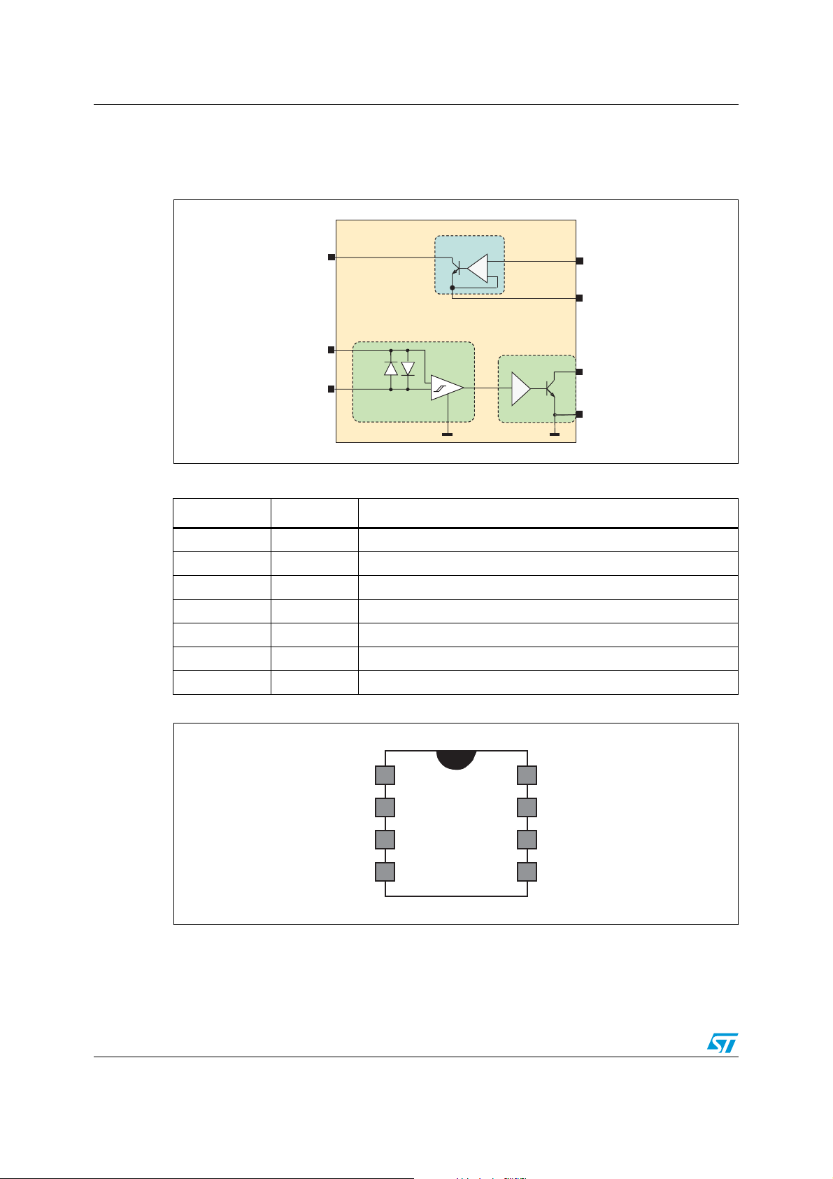
Figure 1. Circuit block diagram
G
V
CC
AC
POWER SWITCH
SIGNAL SHAPING
Table 1. Circuit pin descriptions
GATE DRIVER
+
-
AVF DRIVER
Symbol Type Description
IN SIGNAL Logic AC switch drive
AVF SIGNAL Alternating voltage feedback: AC switch status output
AC SIGNAL AC switch status sense input
V
CC
POWER Positive power supply
G SIGNAL AC switch gate driver output
IN
R
AVF
GND
IG
R
IG
SIGNAL AC switch gate current setting
GND POWER Power supply reference
Figure 2. Pin layout (top view)
IN
IN
AVF
AVF
N/C
N/C
AC
AC
2/13
GND
GND
R
R
IG
IG
G
G
V
V
CC
CC
STCC08 Characteristics
Table 2. Pin allocations
Pin # Name Description
1 IN Logic AC switch drive
2 AVF Alternating voltage feedback: AC switch status output
3 N/C Not connected
4 AC AC switch status sense input
5V
CC
6 G AC switch gate driver output
Positive power supply
7R
IG
AC switch gate current setting
8 GND Power supply reference
Table 3. Absolute ratings (T
= 25 °C unless otherwise stated, respect to GND)
amb
Symbol Pin Parameter name and conditions Value Unit
V
V
V
I
I
CC
IN
I
G
AC
AVF
AVF
V
CC
IN Switch activation voltage -0.3V to VCC +0.3 V
G Sunk driver current 30 mA
AC Input sense current peak 2.2 mA
AVF Alternative feedback voltage -0.3 to V
AVF Maximum feedback current 5 mA
Power supply voltage 0 to 6 V
+0.3 V
CC
Junction temperature range -20 to 125 °C
T
J
Table 4. Recommended operating conditions
All
Storage junction temperature range -40 to 150 °C
Symbol Pin Parameter name and conditions Value Unit
V
CC
I
G
R
IG
V
CC
G Max. sunk driver gate current 28 mA
RIG Gate current setting resistor 30 Ω
Power supply voltage respect to GND 2.97 to 5.5 V
Detector resistance for AC line = 120 V 100 kΩ
R
AC
AC
Detector resistance for AC line = 230 V 300 kΩ
R
SHUNT
T
AMB
T
J
HV biasing resistance for AC line = 120 V 100 kΩ
HV biasing resistance for AC line = 230 V 300 kΩ
All Operating ambient temperature range -20 to 85 °C
All Operating junction temperature range -20 to 125 °C
3/13
Characteristics STCC08
Table 5. Electrical characteristics
Symbol Pin Name Conditions Min Typ Max Unit
Switch drive (respect to GND, Tj=25 °C unless otherwise specified, RIG=30 Ω)
I
QUIESCENTVCC
V
ON
V
OFF
Quiescent current IN = GND 2 mA
On-state switch
IN
activation voltage
Off-state switch
IN
release voltage
0.7*V
CC
0.3*V
CC
V
V
I
IN
I
G
I
AC
V
OH
IN Input drive current Vin > V
G Gate drive current Vin > V
on
on
20 28 mA
AC Detection threshold 82 236 µA
Status output (respect to GND, T
Minimum output
AVF
voltage
=25 °C unless otherwise specified)
j
= 50 µA 0.7*V
I
AVF
I
AVF
= 50 µA
CC
(CMOS Compatible)
V
OL
AVF Maximum drop voltage
I
AVF
= 5 mA
(Opto-transistor
50 µA
0.3*V
CC
1V
compatible)
Table 6. Thermal resistance
Symbol Parameter name and conditions Value Unit
R
TH (j-a)
Table 7. System related electromagnetic compatibility ratings
SMD Thermal resistance Junction to Ambient 140 °C/W
Symbol Node Pin Parameter name and conditions Value Unit
ESD protection, IEC 61000-4-2, per input, against air
V
CC
discharge
Neutral
V
ESD
Gate through ACS; ESD protection, IEC 61000-4-2, pin to
ground, against air discharge
±8 kVG
V
V
Line AC
V
ESD
Neutral V
Neutral
V
PPB
Line AC
1. System oriented test circuits - see Application note AN2716
Alternating current through R
IEC 61000-4-2, pin to ground, against air discharge
ESD protection, IEC 61000-4-2, pin to ground, for contact
CC
discharge
V
Total Peak Pulse Voltage Burst, IEC 61000-4-4
CC
Gate through ACS; Total Peak Pulse Voltage Burst, IEC
G
61000-4-4
(1)
(1)
Alternating current through RAC; Total Peak Pulse Voltage
Burst, IEC 61000-4-4
4/13
(1)
= 300 kΩ; ESD protection,
AC
±6 kV
(1)
±4 kV

STCC08 Functional description
2 Functional description
STCC08 functional description
The STCC08 is a power circuit designed to drive up to 10 mA IGT AC switches and to detect
AC switch failure modes through MCU diagnostic.
It embeds a logic switch driver, an AC switch diode mode detection, a short circuit detection
and an AC switch open detection.
STCC08 can be powered by a 3.3 V or 5 V power supply voltage.
Switch driver
This driver is a logic level buffer (CMOS compatible) interfacing directly with the AC switch
and the microcontroller.
The AC switch must be driven in negative polarity: AC switch COM = A
= V
1
CC
The drive Boolean rule is:
V
> Von: switch = ON
in
V
< Von: switch = OFF
in
The AC switch can be driven in continuous, pulsed or angle phase modes.
In insulated applications, the input can be driven through an opto-coupler powered with a
non-insulated auxiliary power supply.
R
pin allows the AC switch gate current to be set. A resistor must be connected between
IG
this pin and the ground GND. This resistor is defined according to the miminmum ambient
temperature and the AC switch I
(see Figure 3). This optimizes the consumption of the
GT
application.
Figure 3. R
= f(T
ig
130
120
110
100
90
80
70
60
50
40
30
20
10
0
-20 -15 -10 -5 0 5 10 15 20 25 30
amb_min
R
(Ω)
IG_Max
AC switch 10 mA @ 25 °C
AC switch 5 mA @ 25 °C
) for 5/10 mA AC switches
T
_min (°C)
amb
5/13

Functional description STCC08
Failure mode detection
This function detects AC switch failure modes required by the IEC 60335 standard:
● The AC switch diode mode failure in both negative and positive AC line polarities
This failure is simulated with a diode placed in parallel with the power switch according
to the IEC 60335-1 standard.
● The AC switch short-circuit failure mode, any external shorting and any spurious power
switch turn-on
● The open AC switch failure mode
This function improves the system safety. A diode mode failure, a short circuit or an AC
switch open can lead to dangerous situations for the system or the user.
The AVF block monitors the state of the AC switch in both AC polarities. Its output AVF is
transmitted to the MCU for failure detection.
The MCU detects the failure according to the following truth table:
Table 8. STCC08 status truth table with R
IN (MCU generated) AVF MCU DIAGNOSTIC
0 Open collector AC switch OK
in parallel with the load
SHUNT
0 Open collector to 0 toggle Diode mode
0 0 Short AC switch
10AC switch OK
1 Open collector Open AC switch
For a diode mode, the AVF output toggles from open collector to GND each the half of the
AC mains. Therefore, the AVF output is a pulsed signal during a diode mode failure.
The MCU can put the system in a safe configuration, switching off the front end relay
already existing in home appliance designs.
Status reading
The AVF output is an open collector, active at low level. It can either be connected to a MCU
input, in pull up input configuration, or through an opto-coupler in insulated designs.
For inductive loads, there is a phase shift between load current and AC line voltage. When
the ACS control is removed:
● The AC switch - latch structure - still conducts and the AVF is at low level until the next
zero current crossing.
● The AVF is at low level until next zero current crossing.
● In the worst case, the load current crosses zero close to peak mains voltage. Then the
AVF signal should be read at peak mains voltage.
6/13

STCC08 Functional description
Figure 4. Failure mode detection for inductive loads in DC control mode
DIODE MODE
DIODE MODE
DIODE MODE
DIODE MODE
AC LINE
AC LINE
LOAD CURRENT
LOAD CURRENT
IN
AVF
AVF
SUGGESTED
SUGGESTED
READING TIME
READING TIME
NORMAL MODE
NORMAL MODE
NORMAL MODE
NORMAL MODE
SHORT CIRCUIT
SHORT CIRCUIT
SHORT CIRCUIT
SHORT CIRCUIT
The microcontroller can store the AC switch drive signal in a RAM register when it is driving
the STCC08 input. Therefore it can save gate energy while determining conduction state
from this RAM register and multiplexing this information with AVF signal.
AC LINE: High voltage between AC line and neutral
LOAD CURRENT: Current through the AC load
IN: MCU output driving the STCC08 IN input.
AVF: Alternating voltage feedback, output of the STCC08
7/13

Application information STCC08
3 Application information
Figure 5. Application example with an MCU direct drive + ACS
NEUTRAL
ACS
AC
LOAD
SW
R
LINE
SHUNT
R
The placement of a 100 nF capacitor between V
advised. SW is an electromechanical switch that is part of the application design, for
example, the water sensor in a washing machine.
3.1 Recommendations
The STCC08 is designed for 5 and 10 mA ACSs, ACSTs and TRIACs.
STCC08 basic application
G
V
CC
AC
POWER SWITCH
SIGNAL SHAPING
3.3V to 5V
GATE DRIVER
+
-
AVF DRIVER
and GND close to the STCC08 is
CC
IN
R
AVF
AVF
GND
GND
IG
IG
R
V
CC
MCU
V
CC
The microcontroller reads the AC switch state from the AVF output of the STCC08. The
microcontroller can power-off the application driving a front-end relay.
Figure 6. Non-insulated application
NEUTRAL
G
ACS
V
AC
LOAD
SW
R
LINE
SHUNT
R
FRONT END RELAY
8/13
CC
AC
POWER SWITCH
SIGNAL SHAPING
GATE DRIVER
+
-
AVF DRIVER
SAFETY TURN OFF
3.3V to 5V
IN
R
IG
IG
R
AVF
AVF
GND
GND
V
CC
MCU
V
CC

STCC08 Application information
This function is effective whatever the drive and the nature of the load.
Figure 7. ACS benefits
V
NEUTRAL
NEUTRAL
ACS
ACS
G
G
V
V
MAX=VCL
MAX=VCL
R
R
AC1
AC1
V
CC
CC
AC
AC
R
R
AC2
AC2
The ACS clamping capability, from 800 V to 1100 V reduces the stress across R
resistors
AC
during an AC line over-voltage. This provides a robust solution and allows setting high
voltage resistors R
to withstand the ACS clamping voltage instead of the AC line
AC
maximum over-voltage.
STCC08 AVF alarms configuration
Figure 8. Open load and Short circuit ACS discrimination
LINE
NEUTRAL
SHUNT
R
ACS
LOAD
SW
G
V
AC
R
CC
AC
POWER SWITCH
SIGNAL SHAPING
GATE DRIVER
+
-
AVF DRIVER
3.3V to 5V
IN
R
IG
IG
R
AVF
AVF
GND
GND
V
CC
MCU
V
CC
When R
is removed, the MCU cannot discriminate between an ACS short circuit and
SHUNT
open load failure. See Tab l e 9.
9/13

Application information STCC08
Table 9. STCC08 status truth table with R
SHUNT
removed
IN (MCU generated) AVF MCU DIAGNOSTIC
0 Open collector AC switch OK
0 Open collector to 0 toggle Diode mode
0 0 Short circuit or open lead
10AC switch OK
1 Open collector Open AC switch
STCC08 ZVS application
Figure 9. ZVS application schematic
NEUTRAL
ACS
LINE
G
V
CC
R
AC
AC
POWER SWITCH
SIGNAL SHAPING
GATE DRIVER
+
-
AVF DRIVER
3.3V to 5V
IN
IG
R
ZVS
GND
GND
V
CC
V
CC
MCU
The gate driver drives an ACS while the failure detector is used independently for ZVS
detection
10/13

STCC08 Package information
4 Package information
● Epoxy meets UL94, V0
®
In order to meet environmental requirements, ST offers these devices in ECOPACK
packages. These packages have a lead-free second level interconnect. The category of
second level interconnect is marked on the inner box label, in compliance with JEDEC
Standard JESD97. The maximum ratings related to soldering conditions are also marked on
the inner box label. ECOPACK is an ST trademark. ECOPACK specifications are available at
www.st.com.
Table 10. SO-8 dimensions
Dimensions
Seating
Plane
C
A
A2
A1
b
ppp C
8
1
e
D
5
E1
4
C
k
E
Figure 10. Footprint dimensions
in mm(inches)
Ref.
Min. Typ. Max. Min. Typ. Max.
h x 45°
A 1.75 0.069
A1 0.1 0.25 0.004 0.010
A2 1.25 0.049
L
b 0.28 0.48 0.011 0.019
L1
C 0.17 0.23 0.007 0.009
D 4.80 4.90 5.00 0.189 0.193 0.197
E 5.80 6.00 6.20 0.228 0.236 0.244
E1 3.80 3.90 4.00 0.150 0.154 0.157
e 1.27 0.050
h 0.25 0.50 0.010 0.020
L 0.40 1.27 0.016 0.050
L1 1.04 0.041
k0°8°0°8°
ppp 0.10 0.004
Figure 11. Marking
Millimeters Inches
6.8
(0.268)
4.2
(0.165)
0.6
(0.024)
XXXXX : Marking
XXXXX : Marking
ZZ : Manufacturing location
ZZ : Manufacturing location
Y : Year
Y : Year
WW : week
WW : week
x x x x x x
xx xx xx xx xx xx
z z y w w
zz zz yy ww ww
â
â
1.27
(0.050)
Pin 1
Pin 1
11/13

Ordering information STCC08
5 Ordering information
Table 11. Ordering information
Order code Marking Weight Base Qty Delivery Mode
STCC08 STCC08 0.08 g 100 Tube
STCC08RL STCC08 0.08 g 2500 Tape and reel 13”
6 Revision history
Table 12. Document revision history
Date Revision Changes
20-Mar-2008 1 Initial release.
12/13

STCC08
Please Read Carefully:
Information in this document is provided solely in connection with ST products. STMicroelectronics NV and its subsidiaries (“ST”) reserve the
right to make changes, corrections, modifications or improvements, to this document, and the products and services described herein at any
time, without notice.
All ST products are sold pursuant to ST’s terms and conditions of sale.
Purchasers are solely responsible for the choice, selection and use of the ST products and services described herein, and ST assumes no
liability whatsoever relating to the choice, selection or use of the ST products and services described herein.
No license, express or implied, by estoppel or otherwise, to any intellectual property rights is granted under this document. If any part of this
document refers to any third party products or services it shall not be deemed a license grant by ST for the use of such third party products
or services, or any intellectual property contained therein or considered as a warranty covering the use in any manner whatsoever of such
third party products or services or any intellectual property contained therein.
UNLESS OTHERWISE SET FORTH IN ST’S TERMS AND CONDITIONS OF SALE ST DISCLAIMS ANY EXPRESS OR IMPLIED
WARRANTY WITH RESPECT TO THE USE AND/OR SALE OF ST PRODUCTS INCLUDING WITHOUT LIMITATION IMPLIED
WARRANTIES OF MERCHANTABILITY, FITNESS FOR A PARTICULAR PURPOSE (AND THEIR EQUIVALENTS UNDER THE LAWS
OF ANY JURISDICTION), OR INFRINGEMENT OF ANY PATENT, COPYRIGHT OR OTHER INTELLECTUAL PROPERTY RIGHT.
UNLESS EXPRESSLY APPROVED IN WRITING BY AN AUTHORIZED ST REPRESENTATIVE, ST PRODUCTS ARE NOT
RECOMMENDED, AUTHORIZED OR WARRANTED FOR USE IN MILITARY, AIR CRAFT, SPACE, LIFE SAVING, OR LIFE SUSTAINING
APPLICATIONS, NOR IN PRODUCTS OR SYSTEMS WHERE FAILURE OR MALFUNCTION MAY RESULT IN PERSONAL INJURY,
DEATH, OR SEVERE PROPERTY OR ENVIRONMENTAL DAMAGE. ST PRODUCTS WHICH ARE NOT SPECIFIED AS "AUTOMOTIVE
GRADE" MAY ONLY BE USED IN AUTOMOTIVE APPLICATIONS AT USER’S OWN RISK.
Resale of ST products with provisions different from the statements and/or technical features set forth in this document shall immediately void
any warranty granted by ST for the ST product or service described herein and shall not create or extend in any manner whatsoever, any
liability of ST.
ST and the ST logo are trademarks or registered trademarks of ST in various countries.
Information in this document supersedes and replaces all information previously supplied.
The ST logo is a registered trademark of STMicroelectronics. All other names are the property of their respective owners.
© 2008 STMicroelectronics - All rights reserved
STMicroelectronics group of companies
Australia - Belgium - Brazil - Canada - China - Czech Republic - Finland - France - Germany - Hong Kong - India - Israel - Italy - Japan -
Malaysia - Malta - Morocco - Singapore - Spain - Sweden - Switzerland - United Kingdom - United States of America
www.st.com
13/13
 Loading...