

Battery charger with thermal regulation
Feature summary
■ Programmable charge current up to 800mA
■ No external MOSFET, sense resistors or
blocking diode required
■ Constant current / constant voltage operation
with thermal regulation to maximize charge
rate without risk of overheating
■ Charges single cell li-ion batteries directly from
USB port
■ Preset 4.2V charge voltage with 1% accuracy
■ Automatic recharge
■ Single charge status output pin
■ Charge current monitor output for gas gauging
■ C/10 Charge termination
■ 25µA supply current in shutdown mode
■ Low battery voltage detect for precharge
setting
■ Soft-start limits inrush current
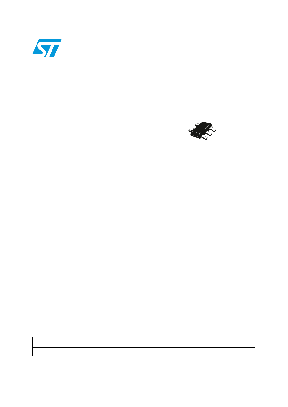
■ TSOT23-5L package
Applications
■ Cellular telephones
■ PDAs
■ Bluetooth applications
■ Battery-powered devices
Description
The STC4054 is a constant current/constant
voltage charger for single cell Li-Ion batteries. No
external sense resistor or blocking diode is
STC4054
800mA Standalone linear Li-Ion
TSOT23-5L
required and its ThinSOT package make it ideally
suited for portable applications.
The STC4054 is designed to work within USB
power specifications. An internal block regulates
the current when the junction temperature
increases, in order to protect the device when it
operates in high power or high ambient
temperature.
The charge voltage is fixed at 4.2V, and the
charge current limitation can be programmed
using a single resistor connectd between PROG
pin and GND. The charge cycle is automatically
terminated when the current flowing to the battery
is 1/10 of the programmed value. If the external
adaptor is removed, the STC4054 turns off and a
2µA current can flow from the battery to the
device. The device can be put into Shutdown
Mode, reducing the supply current to 25µA. The
device also has a charge current monitor, under
voltage lockout, automatic recharge. The device is
packaged in TSOT23-5L.
Order code
Part number Package Packaging
STC4054GR TSOT23-5L 3000 parts per reel
September 2006 Rev. 1 1/17
www.st.com
17

STC4054
Contents
1 Block diagram . . . . . . . . . . . . . . . . . . . . . . . . . . . . . . . . . . . . . . . . . . . . . . 3
2 Pin configuration . . . . . . . . . . . . . . . . . . . . . . . . . . . . . . . . . . . . . . . . . . . 4
3 Maximum ratings . . . . . . . . . . . . . . . . . . . . . . . . . . . . . . . . . . . . . . . . . . . . 5
4 Electrical characteristics . . . . . . . . . . . . . . . . . . . . . . . . . . . . . . . . . . . . . 6
5 Typical performance characteristics . . . . . . . . . . . . . . . . . . . . . . . . . . . . 8
6 Application information . . . . . . . . . . . . . . . . . . . . . . . . . . . . . . . . . . . . . 10
6.1 Charge cycle . . . . . . . . . . . . . . . . . . . . . . . . . . . . . . . . . . . . . . . . . . . . . . 10
6.2 V
6.3 Power ON pin . . . . . . . . . . . . . . . . . . . . . . . . . . . . . . . . . . . . . . . . . . . . . . 10
6.4 CHRG pin . . . . . . . . . . . . . . . . . . . . . . . . . . . . . . . . . . . . . . . . . . . . . . . . . 10
6.5 PROG pin . . . . . . . . . . . . . . . . . . . . . . . . . . . . . . . . . . . . . . . . . . . . . . . . . 11
6.6 Programming charge current . . . . . . . . . . . . . . . . . . . . . . . . . . . . . . . . . . 11
6.7 BAT pin . . . . . . . . . . . . . . . . . . . . . . . . . . . . . . . . . . . . . . . . . . . . . . . . . . . 11
6.8 Charge termination . . . . . . . . . . . . . . . . . . . . . . . . . . . . . . . . . . . . . . . . . . 11
6.9 Automatic recharge . . . . . . . . . . . . . . . . . . . . . . . . . . . . . . . . . . . . . . . . . 11
6.10 Soft start . . . . . . . . . . . . . . . . . . . . . . . . . . . . . . . . . . . . . . . . . . . . . . . . . . 12
6.11 Thermal regulation . . . . . . . . . . . . . . . . . . . . . . . . . . . . . . . . . . . . . . . . . . 12
6.12 Power dissipation . . . . . . . . . . . . . . . . . . . . . . . . . . . . . . . . . . . . . . . . . . . 12
6.13 Stability considerations . . . . . . . . . . . . . . . . . . . . . . . . . . . . . . . . . . . . . . . 12
Pin . . . . . . . . . . . . . . . . . . . . . . . . . . . . . . . . . . . . . . . . . . . . . . . . . . . 10
CC
7 Package mechanical data . . . . . . . . . . . . . . . . . . . . . . . . . . . . . . . . . . . . 13
8 Revision history . . . . . . . . . . . . . . . . . . . . . . . . . . . . . . . . . . . . . . . . . . . 16
2/17
STC4054 Block diagram
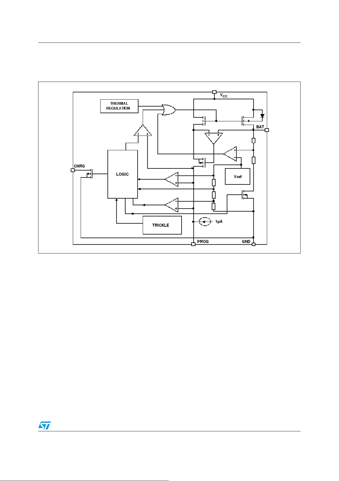
1 Block diagram
Figure 1. Block diagram
3/17
Pin configuration STC4054
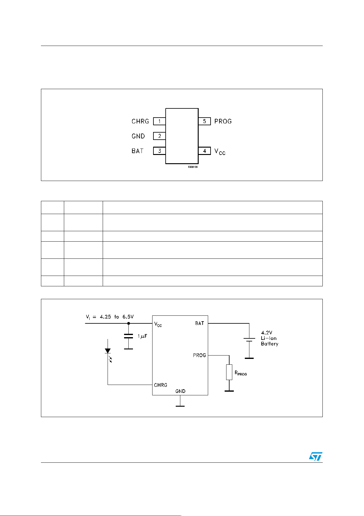
2 Pin configuration
Figure 2. Pin connections (top view)
Table 1. Pin description
Pln N° Symbol Note
1 CHRG
2 GND Ground pin
3BAT
4V
5 PROG Charge current program. Charge Current monitor and Shutdown pin
CC
Open Drain. This pin goes in low impedance when the STC4054 is in precharge or
charge mode
This pin provides an accurate 4.2V output voltage and the charge current to the battery.
Only 2µA reverse current can flow in to the device when in Shutdown mode
Input Supply voltage. The input range is from 4.25V to 6.5V. If VCC<V
device enters Shutdown mode and the sinked I
is less than 2µA
BAT
Figure 3. Application circuit
+30mV the
BAT
4/17
STC4054 Maximum ratings
3 Maximum ratings
Table 2. Absolute maximum ratings
Symbol Parameter Value Unit
V
V
V
PROG
V
CHRG
I
BAT
I
PROG
CC
BAT
Input supply voltage From -0.3 to 10 V
BAT pin voltage From -0.3 to 7 V
PROG pin voltage From -0.3 to VCC+0.3 V
CHRG pin voltage From -0.3 to 7 V
BAT pin current 800 mA
PROG pin current 800 µA
BAT short circuit duration Continuous
T
T
P
D
T
J
STG
OP
Power dissipation Internally Limited mW
Max junction temperature 125 °C
Storage temperature range -65 to 125 °C
Operating junction temperature range -40 to 85 °C
Table 3. Thermal Data
Symbol Parameter Value Unit
R
R
thJC
thJA
Thermal resistance junction-case 81 °C/W
Thermal resistance junction-ambient 255 °C/W
5/17
Electrical characteristics STC4054
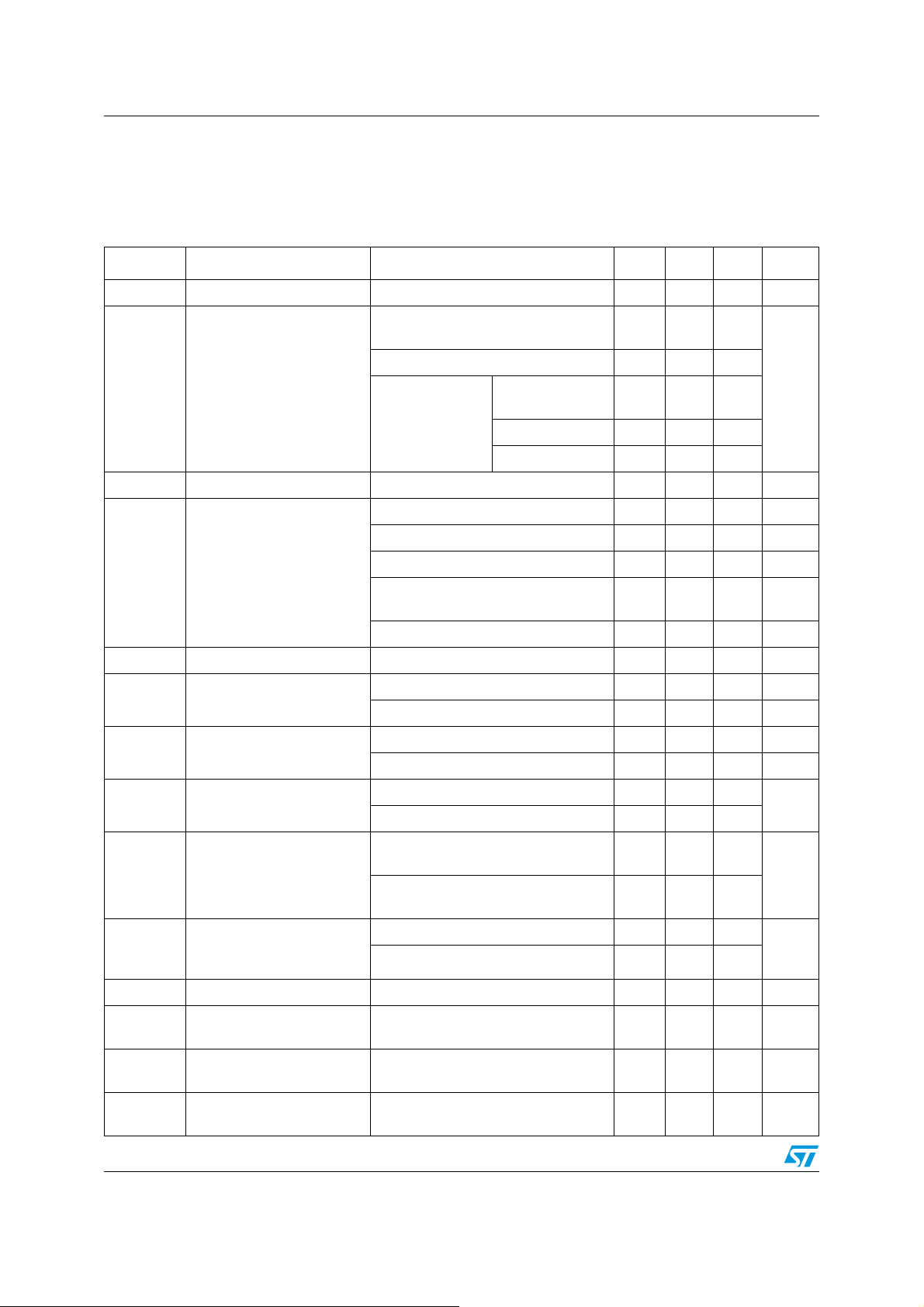
4 Electrical characteristics
Table 4. Electrical characteristics
(V
= 5V, CI = 1µF, TJ = -40 to 85° unless otherwise specified) (
CC
Symbol Parameter Test Min. Typ. Max. Unit
Note 1
).
V
V
V
V
I
I
BAT
I
PRE
V
MSD
CC
CC
BAT
PRE
UV
Supply voltage 4.25 6.5 V
Charge mode, R
= 3.5V
V
BAT
PROG
=10KΩ,
150 500
Standby mode (charge terminated) 150 300
Supply current (
Termination output voltage V
BAT pin current
Pre-charge current V
Pre-charge threshold
VCC Undervoltage lockout
Note 2
)
Shutdown mode
CC
Current mode R
Current mode R
Standby mode V
Shutdown mode (R
connected), T
Sleep mode, V
BAT
R
PROG
Hysteresis R
V
CC
Hysteresis R
= 4.3V to 6.5V, R
PROG
PROG
BAT
=25°C
J
=0V, TJ=25°C ±1 ±2µA
CC
<2.8V R
=10KΩ V
=2KΩ TJ=25°C 20 45 70 mA
PROG
BAT
=10KΩ 70 100 130 mV
PROG
Low to High R
=10KΩ 50 180 300 mV
PROG
not
R
PROG
connected
< V
V
CC
BAT
V
< V
CC
UV
=10KΩ 4.158 4.2 4.242 V
PROG
21 40
17 50
17 40
=10KΩ 90 100 110 mA
=2KΩ 465 500 535 mA
=4.2V 0 -2.5 -6 µA
not
PROG
±1 ±2µA
falling 2.8 2.9 3.0 V
=10KΩ 3.7 3.8 3.9 V
PROG
µA
PROG Pin Rising 1.15 1.21 1.30
Manual shutdown threshold
PROG Pin Falling 0.85 0.95 1.05
V
∆V
6/17
V
ASD
I
TERM
V
PROG
I
CHRG
V
CHRG
RECHRG
Low to High TJ=25°C
V
CC
=10KΩ
R
VCC-V
Lockout threshold
BAT
C/10 Termination current
threshold (I
Note 3
)
(
BAT/IBATC10
)
PROG
V
High to Low TJ=25°C
CC
=10KΩ
R
PROG
R
=10KΩ 0.1
PROG
R
=2KΩ 0.1
PROG
PROG pin voltage Current Mode R
CHRG Pin current weak
pull-down
CHRG Pin pull-down
voltage
Recharger battery threshold
voltage
V
=5V, V
CHRG
R
PROG
I
CHRG
V
FLOAT-VRECHRG
R
PROG
BAT
=10KΩ
=5mA 0.35 0.6 V
=10KΩ
50 85 120
53050
=10KΩ 0.93 1.0 1.07 V
PROG
=4.3V,
, TJ=25°C
82035µA
200 mV
mV
mA/mA

STC4054 Electrical characteristics
Table 4. Electrical characteristics
(V
= 5V, CI = 1µF, TJ = -40 to 85° unless otherwise specified) (
CC
Symbol Parameter Test Min. Typ. Max. Unit
Note 1
).
T
LIM
R
ON
t
SS
T
RECHARGE
t
TERM
I
PROG
Junction temperature in
constant current mode
Power Fet “ON” resistance
(Between V
and BAT)
CC
Soft-start time I
Recharge comparator filter
time
Note 4
Termination comparator
filter time
Note 4
=0 to I
BAT
V
High to Low 0.75 2 4.5 ms
BAT
I
Falling Below I
BAT
=1000V/R
BAT
100 µs
PROG
/10 400 1000 2500 µs
CHG
120 °C
600 mΩ
PROG pin pull-up current 1 µA
Note: 1 The STC4054 was tested using a battery simulator and an output capacitor value about
4.7µF
2 Supply current includes PROG pin current but not include any current delivered to the
battery through the V
3I
is expressed as a fraction of measured full charge current with indicated PROG
TERM
BAT
pin
resistor
4 Guaranteed by design
7/17

Typical performance characteristics STC4054
5 Typical performance characteristics
Figure 4. I
Figure 6. I
vs Supply voltage Figure 5. V
BAT
vs temperature Figure 7. V
BAT
vs V
BAT
PROG
CC
vs temperature
Figure 8. I
8/17
BAT/IPROG
vs temperature Figure 9. I
BAT
vs V
PROG

STC4054 Typical performance characteristics
Figure 10. I
Figure 12. I
BAT/IPROG
CHRG
vs V
CC
vs temperature (CHRG pin
weak pull down current)
Figure 11. V
vs temperature (CHRG pin
CHRG
output low voltage)
Figure 13. Power FET “ON” resistance
Figure 14. I
BAT
vs V
BAT
Figure 15. Recharge battery threshold voltage
vs. temperature
9/17

Application information STC4054
6 Application information
The STC4054 uses an internal P-Channel MOSFET to work in constant current and
constant voltage method. It is able to provide up to 800mA with a final regulated output
voltage of 4.2V
required. It is also possible to use an USB port as power supply voltage.
6.1 Charge cycle
A charge cycle begins when the voltage at the VCC pin rises above the UVLO threshold
level, the R
and when a battery is connected to the charger output. If the battery voltage is below 2.9V,
the charger enters in Trickle Charge mode. In this condition, the device supplies 1/10 of the
programmed charge current to bring the battery voltage up to safe level otherwise the life of
a battery is reduced. If the BAT pin voltage is higher than 2.9V the charger enters in
Constant Current Mode. When the BAT pin voltage is close to the final float voltage (4.2V)
the device enters in Constant Voltage Mode and the charge current begins to decrease. The
charge cycle is terminated when the current drops to 1/10 of the programmed value.
± 1% in full temperature range. No blocking diode and sensing resistor are
program resistor of 1% is connected between the PROG pin to GND pin
PROG
6.2 VCC Pin
Input Supply Voltage. This pin is used to supplie the device in the range from 4.25V to 6.5V
voltage. A bypass capacitor of 1µF is recommended for use. When V
30mV of the BAT pin voltage, the device enters in Shutdown Mode, dropping I
than 2µA.
6.3 CHRG pin
This is a flag open drain. It indicates three different status of the output. When the charge is
in progress this pin is pulled low instead at the end of the charge cycle, a weak pull down of
approximately 20µA is connected to the CHRG pin, indicating a present supply power; if the
flag is forced high impedance an under voltage condition is detected.
6.4 PROG pin
Charge Current Program, Charge Current Monitor and Shutdown Pin. The charge current is
programmed by connecting a 1% resistor, R
constant current, the value of voltage on this pin is 1.0V. In other conditions, the voltage on
this pin can be used to measure the charge current using the following formula:
The PROG pin is used to shut down the device, disconnecting the program resistor from
ground a 1µA current flows to pull the PROG pin high. If the value of this Pin is 1.21V
(shutdown threshold voltage), the device enters Shutdown mode and the input supply
current drops to 25µA. Driving this pin to voltage beyond 2.4V a current of 35µA flows into
the device from PROG pin.
I
BAT
= (V
PROG/RPROG
value drops of
CC
BAT
, to ground. When the device is charging in
PROG
)*1000
to less
10/17

STC4054 Application information
6.5 Programming charge current
The R
1000 times the Prog pin current value. The program resistor and the charge current are
calculated using the following formula:
R
PROG
The charge current out of the BAT pin can be monitored through the PROG pin voltage
using the following equation:
I
=(V
BAT
resistor is used to set the charge current value. The battery charge current is
PROG
=1000*V
PROG/RPROG
PROG/IBAT
;
)x1000
6.6 Charge status indicator (CHRG)
The charge status output has three different states: Strong pull-down (~10mA), weak pulldown (20µA) and high impedance. The strong pull-down indicates that the device is
charging the battery. Weak pull-down indicates that V
device is ready to charge. The last status high impedance indicates an insufficient voltage is
applied to the V
pin or the voltage on VCC is less than 100mV above the BAT pin voltage.
CC
6.7 BAT pin
Charge Current Output pin. It provides charge current to the battery and regulates the final
float voltage to 4.2V. An internal precision resistor is used as a feedback loop to compare
the V
with the reference.
O
meets the UVLO conditions and the
CC
6.8 Charge termination
A charge cycle is terminated when the final float voltage is reached consequently the charge
current falls to 1/10th of the programmed value. The charge is over when the PROG pin
voltage falls below 100mV for longer time than t
off, the device enters in standby mode and the input supply current drops to 200µA.
6.9 Automatic recharge
The device restarts the charge cycle when the battery voltage falls below 4.05V to maintain
the battery capacity value higher than 80%. During the recharge time, the CHRG pin goes
low state.
6.10 Soft start
When a charge cycle starts, a internal soft start circuit minimizes the inrush current. At
starting phase, the charge current ramps from zero to the full scale in a 100µs period time.
(~1ms). The charge current is latched
TERM
11/17

Application information STC4054
6.11 Thermal regulation
An internal thermal feedback loop reduces the output current if the die temperature attempts
to rise above a present value of approximately 120°C. This feature protects the device from
excessive temperature and allows the user to push the limits of the power handling
capability of a given circuit board without risk of damaging the device.
6.12 Power dissipation
It is very important to use a good thermal PC board layout to maximize the available output
current. The thermal path for the heat generated by the IC is from the die to the copper lead
frame through the package leads and exposed pad to the PC board copper. The PC board
copper is the heat sink. The footprint copper pads should be as wide as possible and
expand out to larger copper areas to spread and dissipate the heat to the surrounding
ambient. Feed through vias to inner or backside copper layers are also useful in improving
the overall thermal performance of the device. Other heat sources on the board, not related
to the device, must also be considered when designing a PC board layout because they will
affect overall temperature rise and the maximum output current.
6.13 Stability considerations
The STC4054 contains two control loops: constant voltage and constant current. The
constant-voltage loop is stable without any compensation when a battery is connected with
low impedance leads. Excessive lead length, however, may add enough series inductance
to require a bypass capacitor of at least 1µF from BAT to GND. Furthermore, a 4.7µF
capacitor with a 0.2Ω to 1Ω series resistor from BAT to GND is required to keep ripple
voltage low when the battery is disconnected.
12/17

STC4054 Package mechanical data
7 Package mechanical data
In order to meet environmental requirements, ST offers these devices in ECOPACK®
packages. These packages have a Lead-free second level interconnect. The category of
second Level Interconnect is marked on the package and on the inner box label, in
compliance with JEDEC Standard JESD97. The maximum ratings related to soldering
conditions are also marked on the inner box label. ECOPACK is an ST trademark.
ECOPACK specifications are available at: www.st.com.
13/17

Package mechanical data STC4054
TSOT23-5L MECHANICAL DATA
mm. mils
DIM.
MIN. TYP MAX. MIN. TYP. MAX.
A 1.1 43.3
A1 0 0.1 3.9
A2 0.7 1.0 27.6 39.4
b 0.3 0.5 11.8 19.7
C 0.08 0.2 3.1 7.9
D 2.9 114.2
E 2.8 110.2
E1 1.6 63.0
e0.95 37.4
e1 1.9 74.8
L 0.3 0.6 11.8 23.6
14/17
7282780B

STC4054 Package mechanical data
Tape & Reel SOT23-xL MECHANICAL DATA
DIM.
MIN. TYP MAX. MIN. TYP. MAX.
A 180 7.086
C 12.8 13.0 13.2 0.504 0.512 0.519
D 20.2 0.795
N 60 2.362
T 14.4 0.567
Ao 3.13 3.23 3.33 0.123 0.127 0.131
Bo 3.07 3.17 3.27 0.120 0.124 0.128
Ko 1.27 1.37 1.47 0.050 0.054 0.0.58
Po 3.9 4.0 4.1 0.153 0.157 0.161
P 3.9 4.0 4.1 0.153 0.157 0.161
mm. inch
15/17

Revision history STC4054
8 Revision history
Table 5. Revision history
Date Revision Changes
04-Sep-2006 1 Initial release.
16/17

STC4054
Please Read Carefully:
Information in this document is provided solely in connection with ST products. STMicroelectronics NV and its subsidiaries (“ST”) reserve the
right to make changes, corrections, modifications or improvements, to this document, and the products and services described herein at any
time, without notice.
All ST products are sold pursuant to ST’s terms and conditions of sale.
Purchasers are solely responsible for the choice, selection and use of the ST products and services described herein, and ST assumes no
liability whatsoever relating to the choice, selection or use of the ST products and services described herein.
No license, express or implied, by estoppel or otherwise, to any intellectual property rights is granted under this document. If any part of this
document refers to any third party products or services it shall not be deemed a license grant by ST for the use of such third party products
or services, or any intellectual property contained therein or considered as a warranty covering the use in any manner whatsoever of such
third party products or services or any intellectual property contained therein.
UNLESS OTHERWISE SET FORTH IN ST’S TERMS AND CONDITIONS OF SALE ST DISCLAIMS ANY EXPRESS OR IMPLIED
WARRANTY WITH RESPECT TO THE USE AND/OR SALE OF ST PRODUCTS INCLUDING WITHOUT LIMITATION IMPLIED
WARRANTIES OF MERCHANTABILITY, FITNESS FOR A PARTICULAR PURPOSE (AND THEIR EQUIVALENTS UNDER THE LAWS
OF ANY JURISDICTION), OR INFRINGEMENT OF ANY PATENT, COPYRIGHT OR OTHER INTELLECTUAL PROPERTY RIGHT.
UNLESS EXPRESSLY APPROVED IN WRITING BY AN AUTHORIZED ST REPRESENTATIVE, ST PRODUCTS ARE NOT
RECOMMENDED, AUTHORIZED OR WARRANTED FOR USE IN MILITARY, AIR CRAFT, SPACE, LIFE SAVING, OR LIFE SUSTAINING
APPLICATIONS, NOR IN PRODUCTS OR SYSTEMS WHERE FAILURE OR MALFUNCTION MAY RESULT IN PERSONAL INJURY,
DEATH, OR SEVERE PROPERTY OR ENVIRONMENTAL DAMAGE. ST PRODUCTS WHICH ARE NOT SPECIFIED AS "AUTOMOTIVE
GRADE" MAY ONLY BE USED IN AUTOMOTIVE APPLICATIONS AT USER’S OWN RISK.
Resale of ST products with provisions different from the statements and/or technical features set forth in this document shall immediately void
any warranty granted by ST for the ST product or service described herein and shall not create or extend in any manner whatsoever, any
liability of ST.
ST and the ST logo are trademarks or registered trademarks of ST in various countries.
Information in this document supersedes and replaces all information previously supplied.
The ST logo is a registered trademark of STMicroelectronics. All other names are the property of their respective owners.
© 2006 STMicroelectronics - All rights reserved
STMicroelectronics group of companies
Australia - Belgium - Brazil - Canada - China - Czech Republic - Finland - France - Germany - Hong Kong - India - Israel - Italy - Japan -
Malaysia - Malta - Morocco - Singapore - Spain - Sweden - Switzerland - United Kingdom - United States of America
www.st.com
17/17
 Loading...