


Overvoltage protection device with thermal shutdown
Features
■ Input overvoltage protection up to 28 V
■ Integrated high voltage N-channel MOSFET
switch
■ Low R
■ Integrated charge pump
■ Thermal shutdown protection
■ Softstart feature to control the inrush current
■ Enable input (EN)
■ Fault indication output (FLT)
■ IN input ESD withstand voltage up to ±15 kV
(air discharge), up to ±8 kV (contact discharge)
in typical application circuit with 1µF input
capacitor (±2 kV HBM for standalone device)
■ Certain overvoltage options compliant with the
China Communications Standard YD/T 15912006 (overvoltage protection only)
■ Small, RoHS compliant 2.5 x 2 mm TDFN –
10-lead package.
DS(on)
of 90 mΩ
STBP120
TDFN – 10-lead (2.5 x 2 mm)
Applications
■ Smart phones
■ Digital cameras
■ PDA and palmtop devices
■ MP3 players
■ Low-power handheld devices.
September 2009 Doc ID15492 Rev 5 1/36
www.st.com
1

Contents STBP120
Contents
1 Description . . . . . . . . . . . . . . . . . . . . . . . . . . . . . . . . . . . . . . . . . . . . . . . . . 6
2 Pin descriptions . . . . . . . . . . . . . . . . . . . . . . . . . . . . . . . . . . . . . . . . . . . . 7
2.1 Input (IN) . . . . . . . . . . . . . . . . . . . . . . . . . . . . . . . . . . . . . . . . . . . . . . . . . . 7
2.2 Power output (OUT) . . . . . . . . . . . . . . . . . . . . . . . . . . . . . . . . . . . . . . . . . . 7
2.3 Fault indication output (FLT
2.4 Enable input (EN
2.5 No Connect (NC) . . . . . . . . . . . . . . . . . . . . . . . . . . . . . . . . . . . . . . . . . . . . 8
2.6 Ground (GND) . . . . . . . . . . . . . . . . . . . . . . . . . . . . . . . . . . . . . . . . . . . . . . 8
) . . . . . . . . . . . . . . . . . . . . . . . . . . . . . . . . . . . . . . . . . . . . 8
) . . . . . . . . . . . . . . . . . . . . . . . . . . . . . . . . . . . . 7
3 Operation . . . . . . . . . . . . . . . . . . . . . . . . . . . . . . . . . . . . . . . . . . . . . . . . . 10
3.1 Power-up . . . . . . . . . . . . . . . . . . . . . . . . . . . . . . . . . . . . . . . . . . . . . . . . . 10
3.2 Normal operation . . . . . . . . . . . . . . . . . . . . . . . . . . . . . . . . . . . . . . . . . . . 10
3.3 Undervoltage lockout (UVLO) . . . . . . . . . . . . . . . . . . . . . . . . . . . . . . . . . 10
3.4 Overvoltage lockout (OVLO) . . . . . . . . . . . . . . . . . . . . . . . . . . . . . . . . . . . 11
3.5 Thermal shutdown . . . . . . . . . . . . . . . . . . . . . . . . . . . . . . . . . . . . . . . . . . 11
4 Application information . . . . . . . . . . . . . . . . . . . . . . . . . . . . . . . . . . . . . 12
4.1 Calculating the power dissipation . . . . . . . . . . . . . . . . . . . . . . . . . . . . . . . 12
4.2 Calculating the junction temperature . . . . . . . . . . . . . . . . . . . . . . . . . . . . 12
4.3 PCB layout recommendations . . . . . . . . . . . . . . . . . . . . . . . . . . . . . . . . . 12
5 Maximum rating . . . . . . . . . . . . . . . . . . . . . . . . . . . . . . . . . . . . . . . . . . . . 13
6 DC and AC parameters . . . . . . . . . . . . . . . . . . . . . . . . . . . . . . . . . . . . . . 15
7 Timing diagrams . . . . . . . . . . . . . . . . . . . . . . . . . . . . . . . . . . . . . . . . . . . 17
8 Typical application performance (STBP120DVDK6F) . . . . . . . . . . . . . 19
9 Typical thermal characteristics (STBP120DVDK6F) . . . . . . . . . . . . . . . 24
10 Package mechanical data . . . . . . . . . . . . . . . . . . . . . . . . . . . . . . . . . . . . 28
2/36 Doc ID 15492 Rev 5

STBP120 Contents
11 Tape and reel specification . . . . . . . . . . . . . . . . . . . . . . . . . . . . . . . . . . 30
12 Part numbering . . . . . . . . . . . . . . . . . . . . . . . . . . . . . . . . . . . . . . . . . . . . 33
13 Package marking information . . . . . . . . . . . . . . . . . . . . . . . . . . . . . . . . 34
14 Revision history . . . . . . . . . . . . . . . . . . . . . . . . . . . . . . . . . . . . . . . . . . . 35
Doc ID 15492 Rev 5 3/36

List of tables STBP120
List of tables
Table 1. Pin description and signal names. . . . . . . . . . . . . . . . . . . . . . . . . . . . . . . . . . . . . . . . . . . . . 8
Table 2. Absolute maximum ratings . . . . . . . . . . . . . . . . . . . . . . . . . . . . . . . . . . . . . . . . . . . . . . . . . 13
Table 3. Thermal data. . . . . . . . . . . . . . . . . . . . . . . . . . . . . . . . . . . . . . . . . . . . . . . . . . . . . . . . . . . . 14
Table 4. Operating and AC measurement conditions . . . . . . . . . . . . . . . . . . . . . . . . . . . . . . . . . . . . 15
Table 5. DC and AC characteristics . . . . . . . . . . . . . . . . . . . . . . . . . . . . . . . . . . . . . . . . . . . . . . . . . 15
Table 6. TDFN – 10-lead, 2.5 x 2.0 x 0.75 mm body, pitch 0.50 mm,
package mechanical data dimensions . . . . . . . . . . . . . . . . . . . . . . . . . . . . . . . . . . . . . . . . 29
Table 7. Carrier tape dimensions . . . . . . . . . . . . . . . . . . . . . . . . . . . . . . . . . . . . . . . . . . . . . . . . . . . 30
Table 8. Further tape and reel information . . . . . . . . . . . . . . . . . . . . . . . . . . . . . . . . . . . . . . . . . . . . 30
Table 9. Reel dimensions . . . . . . . . . . . . . . . . . . . . . . . . . . . . . . . . . . . . . . . . . . . . . . . . . . . . . . . . . 31
Table 10. Ordering information scheme . . . . . . . . . . . . . . . . . . . . . . . . . . . . . . . . . . . . . . . . . . . . . . . 33
Table 11. Marking description. . . . . . . . . . . . . . . . . . . . . . . . . . . . . . . . . . . . . . . . . . . . . . . . . . . . . . . 34
Table 12. Document revision history . . . . . . . . . . . . . . . . . . . . . . . . . . . . . . . . . . . . . . . . . . . . . . . . . 35
4/36 Doc ID 15492 Rev 5

STBP120 List of figures
List of figures
Figure 1. Logic diagram . . . . . . . . . . . . . . . . . . . . . . . . . . . . . . . . . . . . . . . . . . . . . . . . . . . . . . . . . . . . 6
Figure 2. Pinout . . . . . . . . . . . . . . . . . . . . . . . . . . . . . . . . . . . . . . . . . . . . . . . . . . . . . . . . . . . . . . . . . . 6
Figure 3. Block diagram . . . . . . . . . . . . . . . . . . . . . . . . . . . . . . . . . . . . . . . . . . . . . . . . . . . . . . . . . . . . 9
Figure 4. Typical application circuit . . . . . . . . . . . . . . . . . . . . . . . . . . . . . . . . . . . . . . . . . . . . . . . . . . . 9
Figure 5. Maximum MOSFET current at T
and T
= 125 °C . . . . . . . . . . . . . . . . . . . . . . . . . . . . . . . . . . . . . . . . . . . . . . . . . . . . . . . . . 14
J
Figure 6. Startup . . . . . . . . . . . . . . . . . . . . . . . . . . . . . . . . . . . . . . . . . . . . . . . . . . . . . . . . . . . . . . . . 17
Figure 7. Overvoltage protection . . . . . . . . . . . . . . . . . . . . . . . . . . . . . . . . . . . . . . . . . . . . . . . . . . . . 17
Figure 8. Disable (EN
Figure 9. FLT
behavior in disable (EN = high) . . . . . . . . . . . . . . . . . . . . . . . . . . . . . . . . . . . . . . . . . . 18
Figure 10. Startup delay, t
Figure 11. FLT
indication delay (OK), t
Figure 12. Output turn-off time, t
Figure 13. FLT
indication delay (FAULT), t
Figure 14. Disable time, t
= high). . . . . . . . . . . . . . . . . . . . . . . . . . . . . . . . . . . . . . . . . . . . . . . . . . . . . . . 18
. . . . . . . . . . . . . . . . . . . . . . . . . . . . . . . . . . . . . . . . . . . . . . . . . . . . . . . . 19
on
. . . . . . . . . . . . . . . . . . . . . . . . . . . . . . . . . . . . . . . . . . . . . . . . . . . 20
off
. . . . . . . . . . . . . . . . . . . . . . . . . . . . . . . . . . . . . . . . . . . . . . . . . . . . . . . . 21
dis
Figure 15. Startup to overvoltage and startup V
Figure 16. Startup inrush current . . . . . . . . . . . . . . . . . . . . . . . . . . . . . . . . . . . . . . . . . . . . . . . . . . . . 22
Figure 17. Output short-circuit . . . . . . . . . . . . . . . . . . . . . . . . . . . . . . . . . . . . . . . . . . . . . . . . . . . . . . . 22
Figure 18. Output short-circuit detail . . . . . . . . . . . . . . . . . . . . . . . . . . . . . . . . . . . . . . . . . . . . . . . . . . 23
Figure 19. I
Figure 20. I
Figure 21. I
Figure 22. V
Figure 23. V
Figure 24. V
Figure 25. R
vs. temperature. . . . . . . . . . . . . . . . . . . . . . . . . . . . . . . . . . . . . . . . . . . . . . . . . . . . . . . 24
CC
CC(STDBY)
CC(UVLO)
OVLO
UVLO
OL(FLT)
DS(on)
vs. temperature . . . . . . . . . . . . . . . . . . . . . . . . . . . . . . . . . . . . . . . . . . . . . . . . . 24
at 2.9 V vs. temperature . . . . . . . . . . . . . . . . . . . . . . . . . . . . . . . . . . . . . . . . . . . 25
vs. temperature . . . . . . . . . . . . . . . . . . . . . . . . . . . . . . . . . . . . . . . . . . . . . . . . . . . . 25
vs. temperature . . . . . . . . . . . . . . . . . . . . . . . . . . . . . . . . . . . . . . . . . . . . . . . . . . . . 26
at 1 mA vs. temperature . . . . . . . . . . . . . . . . . . . . . . . . . . . . . . . . . . . . . . . . . . . . 26
at 1 A vs. temperature . . . . . . . . . . . . . . . . . . . . . . . . . . . . . . . . . . . . . . . . . . . . . . 27
Figure 26. TDFN – 10-lead, 2.5 x 2.0 x 0.75 mm body, pitch 0.50 mm,
package mechanical drawing . . . . . . . . . . . . . . . . . . . . . . . . . . . . . . . . . . . . . . . . . . . . . . . 28
Figure 27. Tape and reel . . . . . . . . . . . . . . . . . . . . . . . . . . . . . . . . . . . . . . . . . . . . . . . . . . . . . . . . . . . 30
Figure 28. Reel dimensions . . . . . . . . . . . . . . . . . . . . . . . . . . . . . . . . . . . . . . . . . . . . . . . . . . . . . . . . . 31
Figure 29. Tape trailer/leader. . . . . . . . . . . . . . . . . . . . . . . . . . . . . . . . . . . . . . . . . . . . . . . . . . . . . . . . 32
Figure 30. Pin 1 orientation . . . . . . . . . . . . . . . . . . . . . . . . . . . . . . . . . . . . . . . . . . . . . . . . . . . . . . . . . 32
= 85 °C for various PCB thermal performance
A
. . . . . . . . . . . . . . . . . . . . . . . . . . . . . . . . . . . . . . . . . . . . . 19
start
. . . . . . . . . . . . . . . . . . . . . . . . . . . . . . . . . . . . . . . . . . 20
stop
delay . . . . . . . . . . . . . . . . . . . . . . . . . . . . . . . 21
O(FLT)
Doc ID15492 Rev 5 5/36
Description STBP120
1 Description
The STBP120 device provides overvoltage protection for input voltage up to +28 V. Its low
R
failures of the DC power supplies in accordance with the China MII Communications
Standard YD/T 1591-2006.
In the event of an input overvoltage condition, the device immediately disconnects the DC
power supply by turning off an internal low R
to protected systems.
In addition, the device also monitors its own junction temperature and switches off the
internal MOSFET if the junction temperature exceeds the specified limit.
The device can be controlled by the microcontroller and can also provide status information
about fault conditions.
The STBP120 is offered in a small, RoHS-compliant TDFN – 10-lead (2.5 mm x 2 mm)
package.
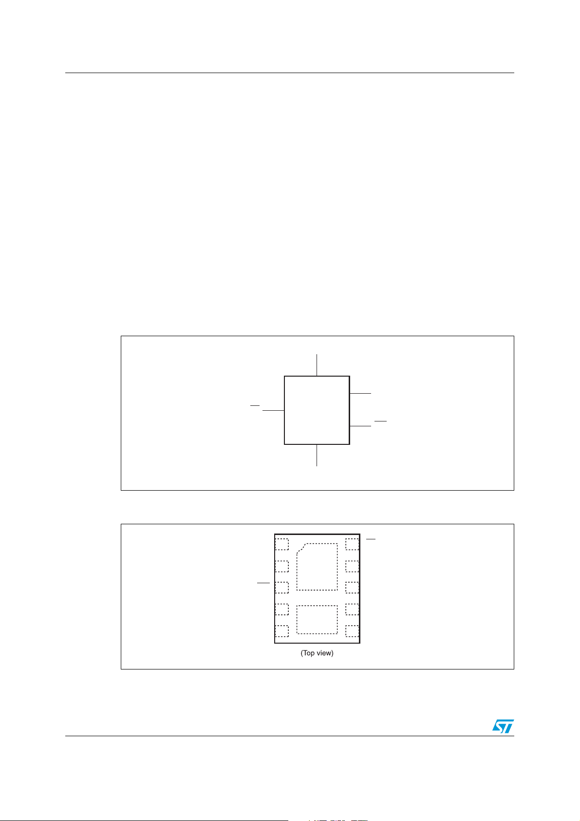
Figure 1. Logic diagram
N-channel MOSFET switch protects the systems connected to the OUT pin against
DS(on)
N-channel MOSFET to prevent damage
DS(on)
Figure 2. Pinout
(1)
IN
1
2
3
4
5
STBP120
GND
PAD1
PAD2
10
9
8
7
6
EN
NC
GND NC
FLT
IN OUT
IN
EN
NC
OUT
OUT
OUT
FLT
AM00240
1. Pin 1, PAD1 and PAD2 are No Connect (NC) and may be tied to IN or GND.
6/36 Doc ID 15492 Rev 5
AM00239

STBP120 Pin descriptions
2 Pin descriptions
2.1 Input (IN)
Input voltage pin. This pin is connected to the DC power supply. External low ESR ceramic
capacitor of minimum value 1 µF must be connected between IN and GND. This capacitor is
for decoupling and also protects the IC against dangerous voltage spikes and ESD events.
This capacitor should be located as close to the IN pins as possible.
All IN pins (4, 5) must be hardwired to common supply.
2.2 Power output (OUT)
Output voltage pin. This pin is connected to the input through a low R
MOSFET switch.
If no fault is detected and the STBP120 is not disabled (controlled by the EN
switch is turned on and the output voltage follows the input voltage.
The output is disconnected from the input when the input voltage is under the UVLO
threshold or above the OVLO threshold, when the chip temperature is above the thermal
shutdown threshold or when the chip is disabled by the EN
There is a 50 ms delay, t
specified range and the power output is connected to the input (see Figure 6).
All OUT pins (6, 7) must be hardwired to common supply.
, between input voltage or junction temperature returns to
on
2.3 Fault indication output (FLT)
The fault indication output (active-low - open-drain) provides information on the STBP120
state to the application controller. When FLT
STBP120 is in the undervoltage or overvoltage condition or thermal shutdown mode is
active. When the input voltage and junction temperature is in specified range, the FLT
is in high impedance (Hi-Z) state.
There is an additional 50 ms delay, t
and the FLT
Since the FLT
the controller supply voltage. If there is no need to use this output, it may be left
disconnected. The suitable R
To improve safety and to prevent damage to application circuits in the event of extreme
voltage or current conditions, an optional protective resistor R
the FLT
to 100 kΩ
output is deactivated (i.e. in Hi-Z state) (see Figure 6).
output is of open-drain type, it may be pulled up by an external resistor RP to
resistor value is in range of 10 kΩ to 1 MΩ .
P
output and the controller input. The suitable R
.
, between the power output is connected to the input
start
N-channel
DS(on)
input), this
input.
is active (i.e. driven low), this indicates the
output
can be connected between
FLT
resistor value is in range of 22 kΩ
FLT
The function of the FLT
output is not affected by the EN input state (see Figure 9).
Doc ID 15492 Rev 5 7/36
Pin descriptions STBP120
2.4 Enable input (EN)
This logical input (active-low) can be used to enable or disable the device. When EN input is
driven high, the STBP120 enters the standby mode and the power output is disconnected
from the input. When EN
limits, the power output is connected to the input.
input is driven low and all operating conditions are within specified
Since the EN
input has no internal pull-down resistor, its logical level must be defined by the
controller or by an external resistor. If there is no need to use this input, it should be
connected to the GND.
To improve safety and to prevent damage to application circuits in the event of extreme
voltage or current conditions, an optional protective resistor R
the EN
100 kΩ
The EN
input and the controller output. The suitable resistor value is in range of 22 kΩ to
.
input level has no impact on the functionality of FLT output (see Figure 8 and
Figure 9).
2.5 No Connect (NC)
Pins 1, 8, 9 and exposed pads PAD1, PAD2 are No Connect. Pin 1 and exposed pads PAD1,
PAD2 may be tied to IN or GND if necessary.
2.6 Ground (GND)
Ground. All voltages are referenced to GND.
Table 1. Pin description and signal names
Pin Name Type Function
can be connected between
EN
1, PAD1, PAD2 NC — No Connect. May be tied to IN or GND.
2 GND Supply Ground
3FLT
4, 5 IN Input / supply Input voltage
6, 7 OUT Output Output voltage
8, 9 NC — No Connect
10 EN
8/36 Doc ID 15492 Rev 5
Output Fault indication output (open-drain)
Input Enable input (no internal pull-down resistor)
STBP120 Pin descriptions
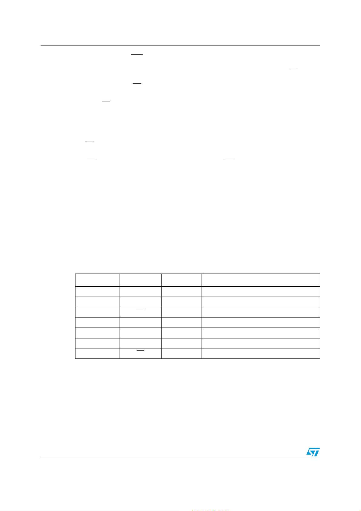
Figure 3. Block diagram
IN
ESD
protection
Core
negative
protection
V
REF
Temperature
detector
SUPPLY
REGULATOR
V
VOLTAGE
REFERENCE
Input overvoltage
Input undervoltage
Thermal shutdown
Figure 4. Typical application circuit
CC
(1),(2)
OSCILLATOR
COUNTERS
CONTROL LOGIC
GND
CHARGE PUMP
MOSFET DRIVER
MCU
INTERFACE
protection
ESD
OUT
OFF
FLT
EN
ESD
protection
AM00306
PERIPHERAL
SYSTEM
AC
adapter
POWERED
PERIPHERALS
1. Optional resistors R
required. Low ESR ceramic capacitor C1 is necessary to ensure proper function of the STBP120. Capacitor C2 is not
CONNECTOR
, R
EN
FLT
OR
prevent damage to the controller under extreme voltage or current conditions and are not
SUPPLY CURRENT
CHARGING CURRENT
IN OUT
C1
1 µF
STBP120
FLT
EN
GND
C2
1 µF
CHARGER
R
FLT
R
EN
DC-DC
EN
IC
ENABLE
BATTERY
PA CK
R
SUPPLY
CIRCUITS
PU
CONTROLLER
APPLICATION
AM00314a
necessary for STBP120 but may be required by the charger IC.
2. The STBP120 MOSFET switch topology allows the current to also flow in the reverse direction, from OUT to IN, which can
be useful for powering external peripherals from the system connector. The charger IC should not contain the reverse
diode to prevent the battery pack voltage from appearing on the system connector. If the reverse current (supply current) is
undesirable, it may be prevented by connecting a Schottky diode in series with the OUT pin. The voltage drop between IN
and charger is increased by the voltage drop across the diode.
Doc ID 15492 Rev 5 9/36

Operation STBP120
3 Operation
The STBP120 provides overvoltage protection for positive input voltage up to 28 V using
a built-in low R
3.1 Power-up
At power-up, with EN = low, the MOSFET switch is turned on after a 50 ms delay, ton, after
the input voltage exceeds the UVLO threshold to ensure the input voltage is stabilized. After
an additional 50 ms delay, t
The FLT
output state is valid for VIN input voltage 1.2 V or higher.
3.2 Normal operation
The device continuously monitors the input voltage and its own internal temperature so the
output voltage is kept within the specified range. Internal MOSFET switch is turned on and
the FLT
The STBP120 enters normal operation state if the input voltage returns to the interval
between V
T
conditions have stabilized. Then, after an additional 50 ms delay, t
deactivated (i.e. driven high). This behavior is equivalent to the startup shown on Figure 6.
output is not active.
UVLO
HYS(OFF)
. Internal MOSFET is turned on after the 50 ms delay ton to ensure that the
N-channel MOSFET switch.
DS(on)
, the FLT indication output is deactivated (see Figure 6).
start
and V
OVLO
- V
HYS(OVLO)
and the junction temperature falls below T
, the FLT output is
start
OFF
-
Note: The STBP120 MOSFET switch topology allows the current to also flow in the reverse
direction, i.e. from OUT to IN, which can be useful e.g. for powering external peripherals
from the system connector (see the supply current in Figure 4). At first, the current flows
through the MOSFET body diode. If the voltage that appears on the IN terminal is above the
UVLO threshold, the MOSFET is (after the 50 ms startup delay) turned on so the voltage
drop across STBP120 is significantly reduced. The charger IC should not contain the
reverse diode to prevent the battery pack voltage from appearing on the system connector.
If the reverse current is undesirable, it may be prevented by connecting a properly rated low
drop Schottky diode in series with the OUT pin. The voltage drop between IN and charger is
increased by the voltage drop across the diode.
Due to the MOSFET body diode, thermal shutdown protection is not functional for the
supply current.
3.3 Undervoltage lockout (UVLO)
To ensure proper operation under any conditions, the STBP120 has an undervoltage lockout
(UVLO) threshold. For rising input voltage, the output remains disconnected from input until
V
voltage exceeds the V
IN
as V
is below the UVLO threshold (assuming the input voltage is above 1.2 V). For falling
IN
input voltage, the UVLO circuit has a 50 mV hysteresis, V
immunity under transient conditions.
threshold (3.25 V typ). The FLT output is driven low as long
UVLO
HYS(UVLO)
, to improve noise
10/36 Doc ID 15492 Rev 5

STBP120 Operation
3.4 Overvoltage lockout (OVLO)
If the input voltage VIN rises above the threshold level V
immediately turned off (see Figure 7). At the same time, the fault indication output FLT
activated (i.e. driven low). This device is equipped with hysteresis, V
noise immunity under transient conditions.
For available OVLO thresholds and hystereses, please see the Ta b l e 5 .
3.5 Thermal shutdown
If the STBP120 internal junction temperature exceeds the T
switch is turned off and the fault indication output FLT
To improve thermal stability, this circuit has a 20 °C hysteresis, T
, the MOSFET switch is
OVLO
threshold, internal MOSFET
OFF
is driven low.
HYS(OFF)
HYS(OVLO)
.
is
, to improve
Doc ID 15492 Rev 5 11/36

Application information STBP120
4 Application information
4.1 Calculating the power dissipation
The maximum power dissipation of the STBP120 internal power MOSFET can be calculated
using following formula:
= I2 x R
P
D
DS(on)(max)
,
Where I is current flowing through the MOSFET and R
MOSFET resistance.
Example:
= 5 Ω, VIN = 5 V, R
R
load
/ (R
I = V
IN
DS(on)(max)
= 0.972 x 0.15 = 0.14 W
P
D
DS(on)(max)
+ R
load
= 150 mΩ
) = 5 / (5 + 0.150) = 0.97 A
The power dissipation of reverse diode (in powering peripherals mode) can be estimated as
P
= (V
D
- VIN) x I ≈ 0.7 x I.
OUT
4.2 Calculating the junction temperature
The maximum junction temperature for given power dissipation, ambient temperature and
thermal resistance junction - to - ambient can be calculated as
= TA + 1.15 x PD x R
T
J
where T
and R
is junction temperature, TA is given ambient temperature, 1.15 is a derating factor
J
is thermal resistance junction - to - ambient, depending on shape, dimension and
thJA
design of PCB. Two examples of PCB with appropriate thermal resistance are listed in
Ta bl e 3 . The junction temperature may not exceed 125 °C (see Table 4), due to T
(thermal shutdown threshold temperature).
= TA + 1.15 x I2 x R
thJA
DS(on)(max)
DS(on)(max)
x R
thJA
is maximum value of
,
OFF
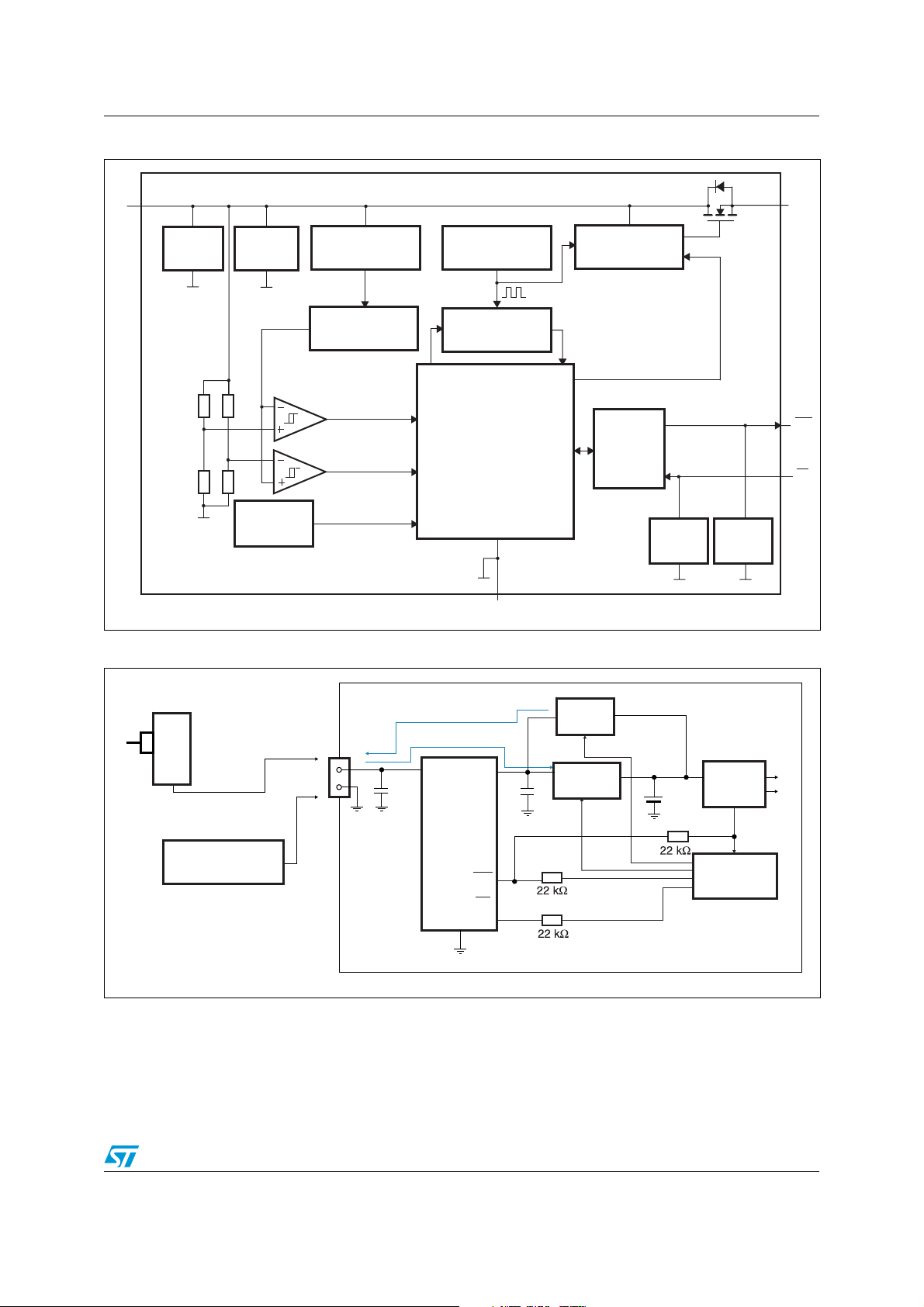
Maximum allowed MOSFET current for ambient temperature T
values are listed in Figure 5.
Example: For conditions listed in previous example, well designed PCB (R
and T
= 85 °C, the maximum junction temperature is
A
85 + 1.15 x 0.14 x 82 = 98.2 °C.
4.3 PCB layout recommendations
● This device is intended as a protection device to the application from overvoltage.
It must be ensured that the clearances between PCB tracks satisfy the high voltage
design rules.
● Input capacitor, C1, should be located as close as possible to the STBP120 device.
It should be a Low-ESR ceramic capacitor. Also the protective resistors R
(if used) should be located close to the STBP120.
● For good thermal performance, it is recommended to connect the STBP120 exposed
thermal pads with the PCB ground plane. In most designs, this requires thermal vias
between the copper pads on PCB and the ground plane.
12/36 Doc ID 15492 Rev 5
= 85 °C and various R
A
= 82 °C/W)
thJA
, REN
FLT
thJA

STBP120 Maximum rating
5 Maximum rating
Stressing the device above the rating listed in the “absolute maximum ratings” table may
cause permanent damage to the device. These are stress ratings only and operation of the
device at these or any other conditions above those indicated in the operating sections of
this specification is not implied. Exposure to absolute maximum rating conditions for
extended periods may affect device reliability. Refer also to the STMicroelectronics SURE
Program and other relevant quality documents.
Table 2. Absolute maximum ratings
Symbol Parameter Value Unit
T
STG
T
SLD
(2)
T
J
T
A
V
IN
V
IO(OUT)
V
IO
I
,
IN
I
OUT(MOSFET)
I
(FLT)
V
ESD
1. Reflow at peak temperature of 260 °C. The time above 255 °C must not exceed 30 seconds.
2. Maximum junction temperature is internally limited by the thermal shutdown circuit (not valid for reverse
current, see Chapter 3.2).
3. System-level value (see Figure 4, C1 ≥ 1 µF low ESR ceramic capacitor).
4. Human body model, 100 pF discharged through a 1.5kΩ resistor according the JESD22/A114
specification.
5. Machine model, 200 pF discharged through all pins according the JES D22/A115 specification.
Storage temperature (VIN off) –55 to 150 C
(1)
Lead solder temperature for 10 seconds 260 C
Operating junction temperature range –40 to 150 C
Operating ambient temperature range –40 to 85 C
Input voltage (pins IN) –0.3 to 30 V
Input / output voltage (pins OUT) –0.3 to 12 V
Input / output voltage (other pins) –0.3 to 7 V
Input / output current through MOSFET (pins IN, OUT) 2000 mA
Output current (pin FLT )15mA
ESD withstand voltage (IEC 61000-4-2, pins IN only)
Human body model (HBM), Model = 2
Machine model (MM), Model = B
(4)
(5)
(3)
±15 (air),
±8 (contact)
2000 V
200 V
kV
Doc ID 15492 Rev 5 13/36
Maximum rating STBP120
.
Table 3. Thermal data
Symbol Parameter Value Unit
(1)
R
thJA
Thermal resistance (junction to ambient)
204
82
(2)
°C/W
R
thJC
1. The package is mounted on a 2-layers (1S) JEDEC board as per JESD51-7 without thermal vias
underneath the exposed pads.
2. The package is mounted on a 4-layers (2S2P) JEDEC board as per JESD51-7 with 2 thermal vias (one
underneath each exposed pad) as per JESD-51-5. Thermal vias connected from exposed pad to 1'st
buried copper plane of PCB.
Thermal resistance (junction to case) 43 °C/W
Figure 5. Maximum MOSFET current at TA = 85 °C for various PCB thermal
I
(MOSFET)
[A]
performance and T
2.10
1.90
1.70
1.50
1.30
1.10
0.90
0.70
50 100 150 200 250 300 350
= 125 °C
J
R
thJA
[˚C/W]
AM00428b
14/36 Doc ID 15492 Rev 5

STBP120 DC and AC parameters
6 DC and AC parameters
This section summarizes the operating measurement conditions, and the DC and AC
characteristics of the device. The parameters in the DC and AC characteristics tables that
follow are derived from tests performed under the measurement conditions summarized in
Ta bl e 4 . Designers should check that the operating conditions in their circuit match the
operating conditions when relying on the quoted parameters.
Table 4. Operating and AC measurement conditions
Parameter Value Unit
Input voltage (V
Ambient operating temperature (T
Junction operating temperature (T
Output load resistance (R
Table 5. DC and AC characteristics
)5V
IN
) –40 to 85 °C
A
) –40 to 125 °C
J
)5Ω
load
Symbol Description Test condition
V
IN
V
UVLO
V
HYS(UVLO)
V
OVL O
V
HYS(OVLO)
R
DS(on)
I
CC
I
CC(STDBY)
I
CC(UVLO)
V
OL(FLT)
I
L(FLT)
V
IL(EN)
V
IH(EN)
I
L(EN)
Input voltage range 1.2 28 V
Input undervoltage
lockout threshold
Undervoltage lockout
hysteresis
V
rises up OVLO threshold, OVLO option A 5.25 5.375 5.50
IN
rises up OVLO threshold, OVLO option B 5.30 5.50 5.70
V
Overvoltage lockout
threshold
IN
rises up OVLO threshold, OVLO option C 5.71 5.90 6.10
V
IN
rises up OVLO threshold, OVLO option D 5.70 6.02 6.40
V
IN
Input overvoltage
hysteresis
IN to OUT resistance EN = 0 V, V
= 5 V, R
IN
Operating current EN = 0 V, no load on OUT, VIN = 5 V 170 250 µA
Standby current EN = 5 V, no load on OUT, VIN = 5 V 96 150 µA
UVLO operating current VIN = 2.9 V 70 100 µA
FLT output low level
voltage
FLT output leakage
current
1.2 V < V
< V
IN
UVLO
> V
V
IN
OVLO
V
, I
(FLT)
SINK(FLT)
EN low level input
voltage
EN high level input
voltage
EN input leakage
current
V
= 0 V or 5 V 5 nA
(EN)
(1)
Min Typ Max Unit
3.1 3.25 3.4 V
20 50 100 mV
V
30 60 90 mV
connected to OUT 90 150 mΩ
load
, I
SINK(FLT)
= 50 µA 20 400 mV
= 1 mA 400 mV
= 5 V 5 nA
0.4 V
1.2 V
Doc ID 15492 Rev 5 15/36

DC and AC parameters STBP120
Table 5. DC and AC characteristics (continued)
Symbol Description Test condition
Timing parameters
Time measured from V
to V
= 0.3 V (see Figure 6)
OUT
Time measured from V
to V
V
increasing from 5.0 V to 8.0 V at 3.0 V/µs,
IN
R
load
V
increasing from 5.0 V to 8.0 V at 3.0 V/µs,
IN
R
load
= 1.2 V (see Figure 6)
(FLT)
IN
connected to OUT. (see Figure 7)
IN
connected to OUT. (see Figure 7)
Time measured from V
to V
< 0.3 V. R
OUT
load
t
t
stop
t
t
t
start
off
dis
on
(2)
(2)
(2)
Startup delay
FLT indication delay
(OK)
Output turn-off time
FLT indication delay
(FAULT)
Disable time
Time measured from V
Time measured from V
(see Figure 8)
Thermal shutdown
T
OFF
T
HYS(OFF)
Thermal shutdown
threshold temperature
Thermal shutdown
hysteresis
(1)
> V
> V
IN
OUT
OVL O
OVLO
(EN)
> V
to V
to V
≥
UVLO
= 0.3 V
OUT
(FLT)
1.2 V
connected to OUT.
Min Typ Max Unit
30 50 70 ms
30 50 70 ms
≤ 0.3 V.
1.5 5 µs
≤ 0.4 V.
1µs
15µs
130 145 °C
20 °C
1. Test conditions described in Table 4 (except where noted).
2. Guaranteed by design. Not tested in production.
16/36 Doc ID 15492 Rev 5

STBP120 Timing diagrams
7 Timing diagrams
Figure 6. Startup
(1)
OVLO
UVLO
V
IN
V
OUT
V
(FLT)
input is low.
1. EN
Figure 7. Overvoltage protection
V
IN
V
OUT
V
(FLT)
0.3 V
1.2 V
(1)
OVLO
UVLO
0.3 V
0.4 V
t
start
t
on
AM00335
t
off
t
stop
AM00336
1. EN
input is low.
Doc ID 15492 Rev 5 17/36

Timing diagrams STBP120
Figure 8. Disable (EN = high)
(1)
1.2 V
V
(EN)
OVLO
V
IN
0.3 V
UVLO
V
OUT
output still indicates the VIN status.
1. FLT
Figure 9. FLT behavior in disable (EN = high)
1.2 V
V
(EN)
OVLO
UVLO
V
IN
1.2 V
V
FLT
t
dis
equiv. to ton + t
AM00337
start
AM00338
18/36 Doc ID 15492 Rev 5

STBP120 Typical application performance (STBP120DVDK6F)
8 Typical application performance (STBP120DVDK6F)
Figure 10. Startup delay, ton
1. No load on the output. The “leakage” on the V
capacitances of the MOSFET switch.
OUT
Figure 11. FLT indication delay (OK), t
trace is a crosstalk caused mainly by the parasitic
start
Doc ID 15492 Rev 5 19/36

Typical application performance (STBP120DVDK6F) STBP120
Figure 12. Output turn-off time, t
1. 5 Ω load on the output.
off
Figure 13. FLT indication delay (FAULT), t
stop
1. 5 Ω load on the output.
20/36 Doc ID 15492 Rev 5

STBP120 Typical application performance (STBP120DVDK6F)
Figure 14. Disable time, t
1. No change in V
2. 5 Ω load on the output.
status during disable.
O(FLT)
dis
Figure 15. Startup to overvoltage and startup V
O(FLT)
delay
1. 5 Ω load on the output.
Doc ID 15492 Rev 5 21/36

Typical application performance (STBP120DVDK6F) STBP120
Figure 16. Startup inrush current
1. Output load 5 Ω in parallel with C = 100 µF, power supply cable inductance 1 µH, power supply cable
resistance 0.3 Ω.
Figure 17. Output short-circuit
1. See also details on Figure 18.
2. Power supply cable inductance 1 µH, power supply cable resistance 0.3 Ω.
22/36 Doc ID 15492 Rev 5

STBP120 Typical application performance (STBP120DVDK6F)
Figure 18. Output short-circuit detail
1. Due to power supply cable impedance, during the output short-circuit the input voltage falls below the
V
threshold, resulting in turning off the power MOSFET and preventing any damage to the
UVLO
components.
2. Power supply cable inductance 1 µH, power supply cable resistance 0.3 Ω.
Doc ID 15492 Rev 5 23/36

Typical thermal characteristics (STBP120DVDK6F) STBP120
9 Typical thermal characteristics (STBP120DVDK6F)
Figure 19. ICC vs. temperature
180
170
160
150
ICC [µA]
140
130
120
110
100
90
80
–50 0 50 100 150
Temperature [˚C]
AM00415
Figure 20. I
I
CC(STDBY)
[µA]
CC(STDBY)
120
110
100
90
vs. temperature
80
70
60
50
40
–50 0 50 100 150
Temperature [˚C]
AM00416
24/36 Doc ID 15492 Rev 5

STBP120 Typical thermal characteristics (STBP120DVDK6F)
Figure 21. I
I
CC(UVLO)
[µA]
Figure 22. V
CC(UVLO)
80.0
70.0
60.0
50.0
40.0
30.0
20.0
at 2.9 V vs. temperature
–50 0 50 100 150
Temperature [˚C]
vs. temperature
OVLO
6.3
AM00417
V
OVLO
6.2
6.1
[V]
6
5.9
5.8
–50 0 50 100 150
Temperature [˚C]
AM00420
Doc ID 15492 Rev 5 25/36

Typical thermal characteristics (STBP120DVDK6F) STBP120
Figure 23. V
3.35
V
UVLO
[V]
3.25
3.15
Figure 24. V
vs. temperature
UVLO
3.4
3.3
3.2
3.1
–50 0 50 100 150
Temperature [˚C]
at 1 mA vs. temperature
OL(FLT)
AM00422
V
OL(FLT)
[V]
0.1
0.09
0.08
0.07
0.06
0.05
0.04
0.03
0.02
0.01
0
–50 0 50 100 150
Temperature [˚C]
AM00424
26/36 Doc ID 15492 Rev 5

STBP120 Typical thermal characteristics (STBP120DVDK6F)
Figure 25. R
140.0
120.0
100.0
R
DS(on)
[mΩ]
80.0
60.0
40.0
20.0
at 1 A vs. temperature
DS(on)
0.0
–50 0 50 100 150
Temperature [˚C]
AM00427
Doc ID 15492 Rev 5 27/36

Package mechanical data STBP120
10 Package mechanical data
In order to meet environmental requirements, ST offers these devices in different grades of
ECOPACK
specifications, grade definitions and product status are available at: www.st.com.
ECOPACK
®
packages, depending on their level of environmental compliance. ECOPACK®
®
is an ST trademark.
Figure 26. TDFN – 10-lead, 2.5 x 2.0 x 0.75 mm body, pitch 0.50 mm,
package mechanical drawing
INDE X AREA
0.10 C
0.10 C
A
0.08 C
LEADS CO PLA NARIT Y
D
2x
0.10 C 2x
TOP VIEW
SIDE VIE W
D2 -2
e
A1
A
B
SEATING
PLANE
E
C
1
PI N#1 ID
IND EX AR EA
0.10 C A B
(x10)
0.195
L
b (x 10)
10
0.0 2 5
0.350
BOTTOM VI EW
28/36 Doc ID 15492 Rev 5
5
K (x10)
E2
0.195
D2- 1
10L_ME

STBP120 Package mechanical data
Table 6. TDFN – 10-lead, 2.5 x 2.0 x 0.75 mm body, pitch 0.50 mm,
package mechanical data dimensions
(mm) (inches)
Symbol
Min. Nom. Max. Min. Nom. Max.
A 0.70 0.75 0.80 0.028 0.030 0.031
A1 0.00 0.02 0.05 0.000 0.001 0.002
b 0.18 0.25 0.30 0.007 0.010 0.012
(1)
Note
D
BSC
2.50 0.098
D2-1 0.53 0.68 0.78 0.021 0.027 0.031
D2-2 0.93 1.08 1.18 0.037 0.043 0.046
E
BSC
2.00 0.079
E2 0.75 0.90 1.00 0.030 0.035 0.039
e 0.50 0.020
L 0.20 0.30 0.40 0.008 0.012 0.016
K0.20 0.008
N10 10
1. Controlling dimension: millimeters.
2. N is the total number of terminals.
(2)
Doc ID 15492 Rev 5 29/36

Tape and reel specification STBP120
11 Tape and reel specification
Figure 27. Tape and reel
P
0
D
T
Top cover
tape
K
0
Table 7. Carrier tape dimensions
Tape
size
WDEPoP2F
Center lines
of cavity
P
2
User direction of feed
E
A
0
B
0
P
1
F
W
12 12.00 ± 0.30 1.50 +0.10 / –0.00 1.75 ± 0.10 4.00 ± 0.10 2.00 ± 0.10 5.50 ± 0.05
Table 8. Further tape and reel information
AM03073v2
Package code W Ao Bo Ko P1 T Bulk Qty.
2 x 2.5mm TDFN 10 lead 12
2.30 ±
0.10
2.80 ±
0.10
30/36 Doc ID 15492 Rev 5
1.10 ±
0.01
4.00 ±
0.10
0.30 ±
0.05
Reel
Diameter
3000 13

STBP120 Tape and reel specification
Figure 28. Reel dimensions
T
40 mm min.
acces hole
at slot location
B
D
A
Full radius
C
N
Tape slot
in core for
tape start
25 mm min width
G measured
at hub
Table 9. Reel dimensions
Tape size A max. B min. C D min. N min. G T max.
12 mm 330 (13 inch) 1.5 13 ± 0.2 20.2 60 12.4 + 2 / – 0 18.4
AM00443
Doc ID 15492 Rev 5 31/36

Tape and reel specification STBP120
Figure 29. Tape trailer/leader
End
To p
cover
tape
No components No componentsComponents
TRAILER
160 mm min.
Figure 30. Pin 1 orientation
Sealed with cover tape
User direction of feed
10 0 mm mi n.
LEADE
400 mm min.
Start
R
AM00444
Direction of feed
Note: 1 Drawings are not to scale.
2 All dimensions are in mm, unless otherwise noted.
32/36 Doc ID 15492 Rev 5
AM00442a

STBP120 Part numbering
12 Part numbering
Table 10. Ordering information scheme
STBP120 D V DK 6 F
Device type
STBP120
Overvoltage threshold
A = 5.375 V
B = 5.50 V
C = 5.90 V
D = 6.02 V
Undervoltage threshold
V = 3.25 V
Package
DK = TDFN – 10-lead, 2.5 x 2 mm
Temperature range
6 = –40 °C to +85 °C
Shipping method
F = ECOPACK
®
package, tape and reel
Note: Other overvoltage thresholds are offered. Minimum order quantities may apply.
Contact local sales office for availability.
Doc ID 15492 Rev 5 33/36

Package marking information STBP120
13 Package marking information
Table 11. Marking description
Part number
STBP120AVxxxx 5.375 P12A
STBP120BVxxxx 5.50 P12B
STBP120CVxxxx 5.90 P12C
STBP120DVxxxx 6.02 P12D
1. Other overvoltage thresholds are offered. Minimum order quantities may apply.
Contact local sales office for availability.
(1)
Overvoltage threshold (V) Topside marking
34/36 Doc ID 15492 Rev 5

STBP120 Revision history
14 Revision history
Table 12. Document revision history
Date Revision Changes
20-Mar-2009 1 Initial release.
07-Apr-2009 2
Updated Section 2, Section 3, Figure 5, t
shipping method in Ta bl e 1 0, added Section 8 and Section 9.
on
and t
in Table 5 and
start
29-Apr- 2009 3 Updated the revision history table - removed the draft revisions.
Updated Features, Section 4.3, Tab le 2 , Figure 5, Ta bl e 5 , Figure 10,
01-Jun-2009 4
Figure 12, Figure 13, Figure 14, Figure 15, Figure 16, Figure 17,
Figure 18, removed Figure 22, Figure 23, Figure 25, Figure 27,
Figure 29, Figure 30, added Section 11: Tape and reel specification.
25-Sep-2009 5
Document reformatted, updated overvoltage threshold option C in
Ta b le 5 , Ta b l e 1 0 and Ta b le 11 .
Doc ID 15492 Rev 5 35/36

STBP120
y
Please Read Carefully:
Informatio n in this document is provided solely in connection with ST products. STMicroelectronics NV and its subsidiaries (“ST”) reserve the
right to make changes, corrections, modifications or improvements, to this document, and the products and services described herein at an
time, without notice.
All ST products are sold pursuant to ST’s terms and conditions of sale.
Purchasers are solely responsible for the choice, selection and use of the ST products and services described herein, and ST assumes no
liability whatsoever relating to the choice, selection or use of the ST products and services described herein.
No license, express or implied, by estoppel or otherwise, to any intellectual property rights is granted under this document. If any part of this
document refers to any third party products or services it shall not be deemed a license grant by ST for the use of such third party products
or services, or any intellectual property contained therein or considered as a warranty covering the use in any manner whatsoever of such
third party products or services or any intellectual property contained therein.
UNLESS OTHERWISE SET FORTH IN ST’S TERMS AND CONDITIONS OF SALE ST DISCLAIMS ANY EXPRESS OR IMPLIED
WARRANTY WITH RESPECT TO THE USE AND/OR SALE OF ST PRODUCTS INCLUDING WITHOUT LIMITATION IMPLIED
WARRANTIES OF MERCHANTABILITY, FITNESS FOR A PARTICULAR PURPOSE (AND THEIR EQUIVALENTS UNDER THE LAWS
OF ANY JURISDICTION), OR INFRINGEMENT OF ANY PATENT, COPYRIGHT OR OTHER INTELLECTUAL PROPERTY RIGHT.
UNLESS EXPRESSLY APPROVED IN WRITING BY AN AUTHORIZED ST REPRESENTATIVE, ST PRODUCTS ARE NOT
RECOMMENDED, AUTHORIZED OR WARRANTED FOR USE IN MILITARY, AIR CRAFT, SPACE, LIFE SAVING, OR LIFE SUSTAINING
APPLICATIONS, NOR IN PRODUCTS OR SYSTEMS WHERE FAILURE OR MALFUNCTION MAY RESULT IN PERSONAL INJURY,
DEATH, OR SEVERE PROPERTY OR ENVIRONMENTAL DAMAGE. ST PRODUCTS WHICH ARE NOT SPECIFIED AS "AUTOMOTIVE
GRADE" MAY ONLY BE USED IN AUTOMOTIVE APPLICATIONS AT USER’S OWN RISK.
Resale of ST products with provisions different from the statements and/or technical features set forth in this document shall immediately void
any warranty granted by ST for the ST product or service described herein and shall not create or extend in any manner whatsoever, any
liability of ST.
ST and the ST logo are trademarks or registered trademarks of ST in various countries.
Information in this document supersedes and replaces all information previously supplied.
The ST logo is a registered trademark of STMicroelectronics. All other names are the property of their respective owners.
© 2009 STMicroelectronics - All rights reserved
STMicroelectronics group of companies
Australia - Belgium - Brazil - Canada - China - Czech Republic - Finland - France - Germany - Hong Kong - India - Israel - Italy - Japan -
Malaysia - Malta - Morocco - Philippines - Singapore - Spain - Sweden - Switzerland - United Kingdom - United States of America
www.st.com
36/36 Doc ID 15492 Rev 5
 Loading...