

现货库存、技术资料、百科信息、热点资讯,精彩尽在鼎好!
1
3
3
N-CHANNEL 100V - 0.019 Ω - 80A D² PAK/TO-220
TYPE
STB60NF10
STP60NF10
■ TYPICAL R
■ EXTREMELY HIGHL dv/dt CAPABILITY
■ 100% AVALANCHE TESTED
■ SURFACE-MOUNTING D²PAK (TO-263)
V
DSS
100 V
100 V
(on) = 0.019 Ω
DS
POWER PACKAGE IN TAPE & REEL
(SUFFIX “T4")
DESCRIPTION
This MOSFET series realized with STMicroelectronics unique STripFET™ process has specifically been designed to minimize input capacitance
and gate charge. It is therefore suitable as primary
switch in advanced high-efficiency, high-frequency
isolated DC-DC converters for Telecom and Computer applications. It is also intended for any applications with low gate drive requirements.
R
DS(on)
< 0.023 Ω
< 0.023 Ω
I
D
80 A
80 A
STB60NF10
STP60NF10
STripFET™ II POWER MOSFET
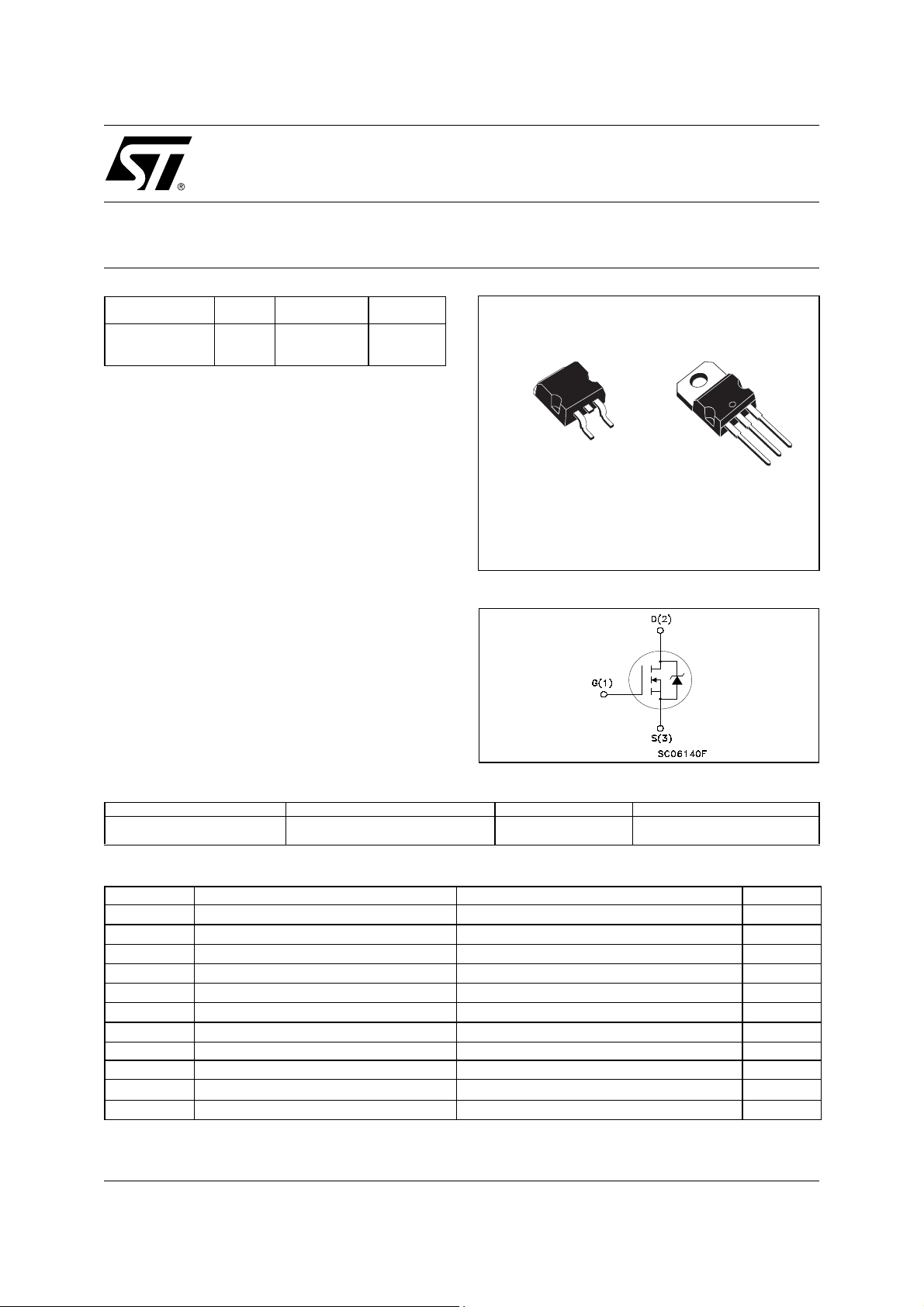
Figure 1:PackageTable 1: General Features
1
D2PAK
TO-263
(Suffix “T4”)
TO-220
Figure 2: Internal Schematic Diagram
2
APPLICATIONS
■ HIGH EFFICIENCY DC/DC CONVERTERS,
INDUSTRIAL, AND LIGHTING EQUIPMENT.
■ MOTOR CONTROL
Table 2: Ordering Information
STB60NF10T4
STP60NF10
SALES TYPE MARKING PACKAGE PACKAGING
B60NF10
P60NF10
TO-263
TO-220
TAPE & REEL
TUBE
Table 3:ABSOLUTE MAXIMUM RATINGS
Symbol Parameter Value Unit
V
DS
V
DGR
V
GS
I
(*) Drain Current (conti nuo us ) at TC = 25°C
D
I
D
I
(•)
DM
P
tot
dv/dt
E
AS
T
stg
(•) Pulse width limited by safe operating area.
(**) Current Limited by Package
Drain-source Voltage (VGS = 0)
Drain-gate Voltage (RGS = 20 kΩ)
100 V
100 V
Gate- source Voltage ± 20 V
80 A
Drain Current (conti nuo us ) at TC = 100°C
66 A
Drain Current (pulse d) 320 A
Total Dissipation at TC = 25°C
300 W
Derating Factor 2 W/°C
(1)
Peak Diode Recove ry vo ltag e slo pe 16 V/ns
(2)
Single Pulse Avalanche Energy 485 mJ
Storage Temperature -55 to 175 °C
(1) ISD ≤80A, di/dt ≤300A/µs, VDD ≤ V
(2) Starting Tj = 25 oC, ID = 40A, VDD = 30V
(BR)DSS
, Tj ≤ T
JMAX
Rev. 2.0
1/10May 2005
STB60NF10 STP60NF10
Table 4: THERMAL DATA
Rthj-case
Rthj-amb
T
Thermal Resistance Junction-case
Thermal Resistance Junction-ambient
Maximum Lead Temperature For Soldering Purpose
l
Max
Max
0.5
62.5
300
°C/W
°C/W
°C
ELECTRICAL CHARACTERISTICS (T
= 25 °C unless otherwise specified)
case
Table 5: OFF
Symbol Parameter Test Conditions Min. Typ. Max. Unit
I
V
(BR)DSS
Drain-source
= 250 µA, VGS = 0
D
100 V
Breakdown Voltage
V
I
DSS
I
GSS
Table 6: ON
Zero Gate Voltage
Drain Current (V
Gate-body Leakage
Current (V
(*)
DS
= 0)
GS
= 0)
= Max Rating
DS
= Max Rating TC = 125°C
V
DS
= ± 20 V
V
GS
1
10
±100 nA
Symbol Parameter Test Conditions Min. Typ. Max. Unit
V
GS(th)
R
DS(on)
Gate Threshold Voltage
Static Drain-source On
V
= VGS ID = 250 µA
DS
V
= 10 V ID = 40 A
GS
234V
0.019 0.023 Ω
Resistance
Table 7: DYNAMIC
Symbol Parameter Test Conditions Min. Typ. Max. Unit
(*)
g
fs
C
iss
C
oss
C
rss
Forward Transconductance
Input Capacitance
Output Capacitance
Reverse Transfer
Capacitance
V
25 V ID=40 A
DS =
V
= 25V f = 1 MHz VGS = 0
DS
78 S
4270
470
140
µA
µA
pF
pF
pF
2/10
STB60NF10 STP60NF10
ELECTRICAL CHARACTERISTICS (continued)
Table 8: SWITCHING ON
Symbol Parameter Test Conditions Min. Typ. Max. Unit
V
t
d(on)
Q
Q
Q
t
r
g
gs
gd
Turn-on Delay Time
Rise Time
Total Gate Charge
Gate-Source Charg e
Gate-Drain Charge
Table 9: SWITCHING OFF
Symbol Parameter Test Conditions Min. Typ. Max. Unit
t
d(off)
t
f
Turn-off Delay Time
Fall Time
Table 10: SOURCE DRAIN DIODE
Symbol Parameter Test Conditions Min. Typ. Max. Unit
I
SD
I
SDM
V
SD
t
rr
Q
rr
I
RRM
(*)
Pulsed: Pulse duration = 300 µs, duty cycle 1.5 %.
(
•)Pulse width limited by safe operating area.
Source-drain Curre nt
)
Source-drain Curre nt (pu lse d)
(•
(*)
Forward On Voltage
Reverse Recovery Time
Reverse Recovery Charge
Reverse Recovery Current
= 50 V ID = 40 A
DD
=4.7 Ω VGS = 10 V
R
G
(Resistive Load, Figu re )
V
= 50V ID= 80A VGS= 10V
DD
V
= 50 V ID = 40 A
DD
=4.7Ω, V
R
G
GS
= 10 V
(Resistive Load, Figu re 3)
I
= 80 A VGS = 0
SD
I
= 80 A di/dt = 100A/µs
SD
= 50 V Tj = 150°C
V
DD
(see test circuit, Figure 5)
17
56
104
20
32
82
23
80
320
1.3 V
92
340
7.4
ns
ns
nC
nC
nC
ns
ns
A
A
ns
µC
A
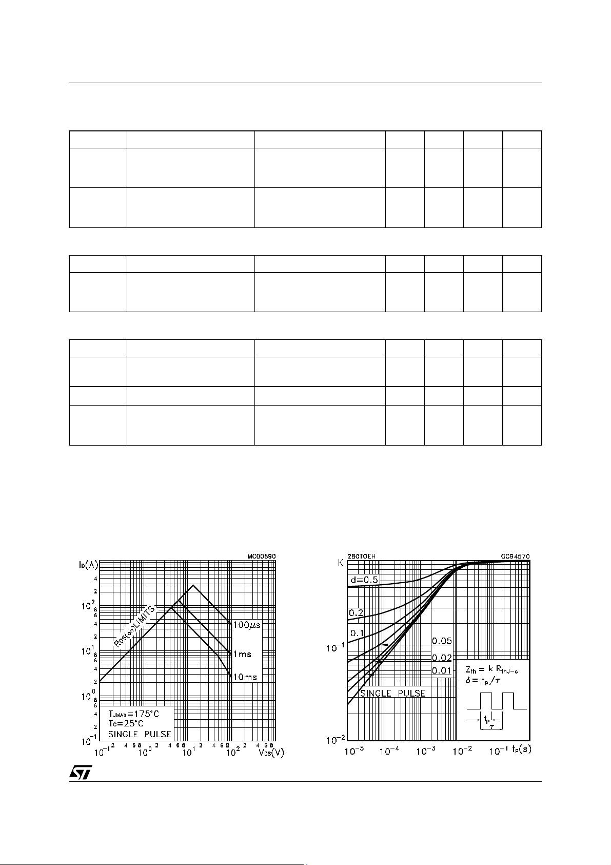
Figure 3: Safe Operating Area
Figure 4: Thermal Impedance
3/10

STB60NF10 STP60NF10
Figure 5: Output Characteristics Figure 6: Transfer Characteristics
Figure 7: Transconductance Figure 8: Static Drain-source On Resistance
Figure 9: Gate Charge vs Gate-source Voltage Figure 10: Capa cita nc e Va riat ion s
4/10

STB60NF10 STP60NF10
Figure 11: Normalized Gate Threshold Voltage vs
Temperature
Figure 13: Source-d rain Diod e For wa rd Ch ara ct eris tic s Figure 14: Normalized Breakdown Voltage vs
Figure 12: Normalized on Resistance vs Temperature
Temperature.
. .
.
.
5/10

STB60NF10 STP60NF10
Figure 15: Unclamped Inductive Load Test Circuit
Figure 17: Switching Times Test Circuits For Resis-
tive Load
Figure 16: Unclamped Inductive Waveform
Figure 18: Gate Charge test Circuit
Figure 19: Test Ci rcuit For Inductiv e Load Switch-
ing And Diode Recovery Times
6/10

D2PAK MECHANICAL DATA
STB60NF10 STP60NF10
DIM.
A 4.4 4.6 0.173 0.181
A1 2.49 2.69 0.098
A2 0.03 0.23 0.001 0.009
B 0.7 0.93 0.028 0.037
B2 1.14 1.7 0.045 0.067
C 0.45 0.6 0.018 0.024
C2 1.21 1.36 0.048 0.054
D 8.95 9.35 0.352 0.368
D1 8 0.315
E 10 10.4 0.394 0.409
E1 8.5 0.334
G 4.88 5.28 0.192 0.208
L 15 15.85 0.591 0.624
L2 1.27 1.4 0.050 0.055
L3 1.4 1.75 0.055 0.069
M 2.4 3.2 0.094 0.126
R 0.4 0.015
V2 0° 8° 0° 8°
MIN. TYP. MAX. MIN. TYP. TYP.
mm. inch.
0.106
7/10

STB60NF10 STP60NF10
TO-220 MECHANICAL DATA
DIM.
A 4.4 4.6 0.173 0.181
C 1.23 1.32 0.048 0.051
D 2.40 2.72 0.094 0.107
E 0.49 0.70 0.019 0.027
F 0.61 0.88 0.024 0.034
F1 1.14 1.70 0.044 0.067
F2 1.14 1.70 0.044 0.067
G 4.95 5.15 0.194 0.203
G1 2.40 2.70 0.094 0.106
H2 10 10.40 0.393 0.409
L2 16.40 0.645
L3 28.90 1.137
L4 13 14 0.511 0.551
L5 2.65 2.95 0.104 0.116
L6 15.25 15.75 0.600 0.620
L7 6.20 6.60 0.244 0.260
L9 3.50 3.93 0.137 0.154
DIA 3.75 3.85 0.147 0.151
MIN. TYP. MAX. MIN. TYP. TYP.
mm. inch.
8/10

Table 11:Revision History
Date Revision Description of Changes
STB60NF10 STP60NF10
May 2005
May 2005 2.0 ADDED PACKAGE D²PAK
1.0 FIRST ISSUE
9/10

STB60NF10 STP60NF10
I
s
o
d
b
ct
t
ot
a
nformation furnished is believed to be accurate and reliable. However, STMicroelectronics assumes no responsibility for the consequence
f use of such information nor for any infrin gement of patents or other rights of third parties which may resul t from its use. No license is grant e
y implication or otherwise under any patent or patent rights of STMicroelectronics. Specifications mentioned in this publication are subje
o change without notic e. This publication supersedes and replaces all information previously supplied. ST Microelectronics products are n
uthorized for use as critical components in life support devices or systems without express written approval of STMicroelectronics.
The ST logo is registered trademark of STMicroelectronics
All other names are the property of their respective owners.
© 2005 STMicroelectronics - All Rights Reserved
Australia - Belgium - Brazil - Canada - China - Czech Republic - Finland - France - Germany - Hong Kong - India - Israel - Italy - Japan -
Malaysia - Malta - Morocco -Singapore - Spain - Sweden - Switzerland - United Kingdom - United States of Americ a.
STMicroelectronics group of comp anies
www.st.com
10/10
 Loading...