

STB5701
350 to 400 MHz FSK/ASK receiver
(ST-RECORD01 family)
Preliminary Data
Features
■ Multiband receiver: 350MHz to 400MHz
■ FSK/ASK modulation selection
■ Programmable multichannel
■ High dynamic range with On-Chip AGC
■ PLL and fully VCO integrated
■ Image Rejection Mixer integrated
■ Start Code Detector block (SCD)
■ I2C serial interface (standard mode/fast mode)
■ BiCMOS SiGe technology
■ VQFN package 5 x 5 mm
Applications
■ 350 to 400 MHz ISM Band System
■ Set Top Box
Table 1. Device summary
Description
This device is a single chip FSK/ASK receiver
optimized for licence-free ISM band operations
from 350MHz to 400 MHz. It can easily be
configured to provide the optimal solution for the
user's application like Set Top Box and 350/400
MHz ISM Band Systems.
Order codes
Package
Tray Tape & Reel
QFN32L STB5701 STB5701TR
October 2007 Rev 1 1/35
This is preliminary information on a new product now in development or undergoing evaluation. Details are subject to
change without notice.
www.st.com
35

Contents STB5701
Contents
1 Block diagram and pin configuration . . . . . . . . . . . . . . . . . . . . . . . . . . . 6
2 Electrical specifications . . . . . . . . . . . . . . . . . . . . . . . . . . . . . . . . . . . . . 13
2.1 Absolute maximum ratings . . . . . . . . . . . . . . . . . . . . . . . . . . . . . . . . . . . . 13
2.2 Thermal data . . . . . . . . . . . . . . . . . . . . . . . . . . . . . . . . . . . . . . . . . . . . . . 13
3 Electrical characteristics . . . . . . . . . . . . . . . . . . . . . . . . . . . . . . . . . . . . 14
4 Functional description . . . . . . . . . . . . . . . . . . . . . . . . . . . . . . . . . . . . . . 17
4.1 General description . . . . . . . . . . . . . . . . . . . . . . . . . . . . . . . . . . . . . . . . . 17
4.2 Programmable Phase Locked Loop synthesizer (PLL) . . . . . . . . . . . . . . 18
4.2.1 Divider (a-counter, m-counter and prescaler) . . . . . . . . . . . . . . . . . . . . 18
4.2.2 Reference divider . . . . . . . . . . . . . . . . . . . . . . . . . . . . . . . . . . . . . . . . . . 19
4.2.3 Phase Frequency Detector . . . . . . . . . . . . . . . . . . . . . . . . . . . . . . . . . . 19
4.2.4 Loop filter . . . . . . . . . . . . . . . . . . . . . . . . . . . . . . . . . . . . . . . . . . . . . . . . 20
4.3 Receiver section . . . . . . . . . . . . . . . . . . . . . . . . . . . . . . . . . . . . . . . . . . . . 20
4.3.1 Low Noise Amplifier (LNA) . . . . . . . . . . . . . . . . . . . . . . . . . . . . . . . . . . . 20
4.3.2 Image Rejection Mixer . . . . . . . . . . . . . . . . . . . . . . . . . . . . . . . . . . . . . . 21
4.3.3 ASK/FSK demodulator and data filter . . . . . . . . . . . . . . . . . . . . . . . . . . 21
4.3.4 Min /Max peak detector . . . . . . . . . . . . . . . . . . . . . . . . . . . . . . . . . . . . . 23
4.3.5 Data slicer . . . . . . . . . . . . . . . . . . . . . . . . . . . . . . . . . . . . . . . . . . . . . . . 23
4.4 Digital control and source selection . . . . . . . . . . . . . . . . . . . . . . . . . . . . . 23
4.4.1 State pin . . . . . . . . . . . . . . . . . . . . . . . . . . . . . . . . . . . . . . . . . . . . . . . . . 24
4.4.2 Data pin . . . . . . . . . . . . . . . . . . . . . . . . . . . . . . . . . . . . . . . . . . . . . . . . . 24
4.4.3 MODE register . . . . . . . . . . . . . . . . . . . . . . . . . . . . . . . . . . . . . . . . . . . . 24
4.5 Start code detection example . . . . . . . . . . . . . . . . . . . . . . . . . . . . . . . . . . 25
4.6 Registers list . . . . . . . . . . . . . . . . . . . . . . . . . . . . . . . . . . . . . . . . . . . . . . . 26
4.7 Register summary . . . . . . . . . . . . . . . . . . . . . . . . . . . . . . . . . . . . . . . . . . 26
4.8 Detailed display description . . . . . . . . . . . . . . . . . . . . . . . . . . . . . . . . . . . 27
5 Package information . . . . . . . . . . . . . . . . . . . . . . . . . . . . . . . . . . . . . . . . 32
5.1 ECOPACK® packages . . . . . . . . . . . . . . . . . . . . . . . . . . . . . . . . . . . . . . . 32
5.2 QFN32L (5mm x 5mm) information . . . . . . . . . . . . . . . . . . . . . . . . . . . . . 32
2/35

STB5701 Contents
6 Revision history . . . . . . . . . . . . . . . . . . . . . . . . . . . . . . . . . . . . . . . . . . . 34
3/35

List of tables STB5701
List of tables
Table 1. Device summary . . . . . . . . . . . . . . . . . . . . . . . . . . . . . . . . . . . . . . . . . . . . . . . . . . . . . . . . . . 1
Table 2. Pin description . . . . . . . . . . . . . . . . . . . . . . . . . . . . . . . . . . . . . . . . . . . . . . . . . . . . . . . . . . . 6
Table 3. Bill of material . . . . . . . . . . . . . . . . . . . . . . . . . . . . . . . . . . . . . . . . . . . . . . . . . . . . . . . . . . . 11
Table 4. Absolute maximum ratings (Tamb = 25oC) . . . . . . . . . . . . . . . . . . . . . . . . . . . . . . . . . . . . 12
Table 5. Thermal data. . . . . . . . . . . . . . . . . . . . . . . . . . . . . . . . . . . . . . . . . . . . . . . . . . . . . . . . . . . . 12
Table 6. Electrical characteristics . . . . . . . . . . . . . . . . . . . . . . . . . . . . . . . . . . . . . . . . . . . . . . . . . . . 13
Table 7. I2C reserved addresses . . . . . . . . . . . . . . . . . . . . . . . . . . . . . . . . . . . . . . . . . . . . . . . . . . . 25
Table 8. I2C address breakdown . . . . . . . . . . . . . . . . . . . . . . . . . . . . . . . . . . . . . . . . . . . . . . . . . . . 25
Table 9. I2C mapped top level registers - summary . . . . . . . . . . . . . . . . . . . . . . . . . . . . . . . . . . . . . 25
Table 10. I2C mapped SCD registers - summary . . . . . . . . . . . . . . . . . . . . . . . . . . . . . . . . . . . . . . . . 25
Table 11. DIG_config register format . . . . . . . . . . . . . . . . . . . . . . . . . . . . . . . . . . . . . . . . . . . . . . . . . 26
Table 12. RF_Config register format . . . . . . . . . . . . . . . . . . . . . . . . . . . . . . . . . . . . . . . . . . . . . . . . . 26
Table 13. PLL_A register . . . . . . . . . . . . . . . . . . . . . . . . . . . . . . . . . . . . . . . . . . . . . . . . . . . . . . . . . . 27
Table 14. PLL_M register format . . . . . . . . . . . . . . . . . . . . . . . . . . . . . . . . . . . . . . . . . . . . . . . . . . . . 27
Table 15. PLL_R register format. . . . . . . . . . . . . . . . . . . . . . . . . . . . . . . . . . . . . . . . . . . . . . . . . . . . . 27
Table 16. SCD_config register format . . . . . . . . . . . . . . . . . . . . . . . . . . . . . . . . . . . . . . . . . . . . . . . . 27
Table 17. SCD_status register format . . . . . . . . . . . . . . . . . . . . . . . . . . . . . . . . . . . . . . . . . . . . . . . . 28
Table 18. SCD_code register format . . . . . . . . . . . . . . . . . . . . . . . . . . . . . . . . . . . . . . . . . . . . . . . . . 28
Table 19. SCD_code_lenth register format . . . . . . . . . . . . . . . . . . . . . . . . . . . . . . . . . . . . . . . . . . . . 28
Table 20. SCD_symbol_min_time register format . . . . . . . . . . . . . . . . . . . . . . . . . . . . . . . . . . . . . . . 28
Table 21. SCD_symbol_max_time register format . . . . . . . . . . . . . . . . . . . . . . . . . . . . . . . . . . . . . . . 29
Table 22. SCD_symbol_nom_time register format . . . . . . . . . . . . . . . . . . . . . . . . . . . . . . . . . . . . . . . 29
Table 23. SCD_prescaler register format . . . . . . . . . . . . . . . . . . . . . . . . . . . . . . . . . . . . . . . . . . . . . . 29
Table 24. Interrupt_enable register format . . . . . . . . . . . . . . . . . . . . . . . . . . . . . . . . . . . . . . . . . . . . . 29
Table 25. Interrupt_clear register format . . . . . . . . . . . . . . . . . . . . . . . . . . . . . . . . . . . . . . . . . . . . . . 30
Table 26. Timeout register format. . . . . . . . . . . . . . . . . . . . . . . . . . . . . . . . . . . . . . . . . . . . . . . . . . . . 30
Table 27. QFN32L (5mm x 5mm) mechanical data . . . . . . . . . . . . . . . . . . . . . . . . . . . . . . . . . . . . . . 32
Table 28. Document revision history . . . . . . . . . . . . . . . . . . . . . . . . . . . . . . . . . . . . . . . . . . . . . . . . . 33
4/35

STB5701 List of figures
List of figures
Figure 1. Block diagram . . . . . . . . . . . . . . . . . . . . . . . . . . . . . . . . . . . . . . . . . . . . . . . . . . . . . . . . . . . . 5
Figure 2. Test circuit . . . . . . . . . . . . . . . . . . . . . . . . . . . . . . . . . . . . . . . . . . . . . . . . . . . . . . . . . . . . . 10
Figure 3. PLL block diagram . . . . . . . . . . . . . . . . . . . . . . . . . . . . . . . . . . . . . . . . . . . . . . . . . . . . . . . 17
Figure 4. LNA block diagram . . . . . . . . . . . . . . . . . . . . . . . . . . . . . . . . . . . . . . . . . . . . . . . . . . . . . . 19
Figure 5. Mixer block diagram . . . . . . . . . . . . . . . . . . . . . . . . . . . . . . . . . . . . . . . . . . . . . . . . . . . . . . 20
Figure 6. ASK/FSK demodulator block diagram . . . . . . . . . . . . . . . . . . . . . . . . . . . . . . . . . . . . . . . . 21
Figure 7. Digital section block diagram . . . . . . . . . . . . . . . . . . . . . . . . . . . . . . . . . . . . . . . . . . . . . . . 22
Figure 8. START code . . . . . . . . . . . . . . . . . . . . . . . . . . . . . . . . . . . . . . . . . . . . . . . . . . . . . . . . . . . . 24
Figure 9. QFN32L (5mm x 5mm) dimensions . . . . . . . . . . . . . . . . . . . . . . . . . . . . . . . . . . . . . . . . . . 31
5/35
Block diagram and pin configuration STB5701
10
(
)
K
K
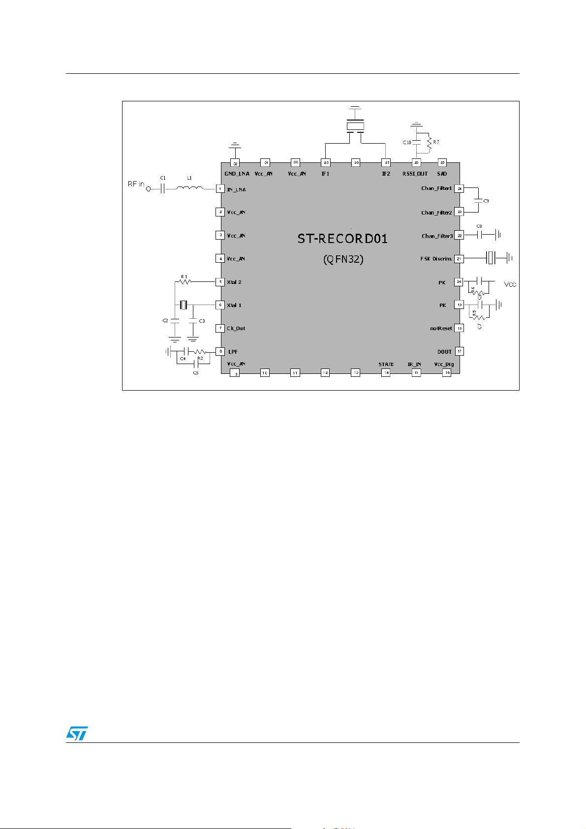
1 Block diagram and pin configuration
Figure 1. Block diagram
cc
cc
V
V
MHz
1
Chan_Filter1 (24)
21
Pin
FSK_Discr
(25)
SAD
FSK
(26)
RSSI_OUT
2
IF
(27)
MHz
.7
Ceramic Filter
(28)
(29)
TEST_EN
1
IF
I
s
Demodulator
Q
s
Chan_Filter2 (23)
Chan_Filter3 (22)
FSK
ASK
I2C
RSSI
(ASK_NOTFSK)
10.7
FSK_Discr
(21)
P
(20)
Discriminator
Min
Peak
Mean
Data Slicer
25
Pin
SAD
28
Pin
Test_ EN
Clk
Digital
Section
VCO
: 2
18
2
DOUT (17)
notReset
P
(19)
Max
Detector
Vcc_Dig
(16)
SCD
I2C
Interface
TANK
IR_IN
(15)
STATE
(14)
SDA
(13)
SCL
(12)
11
NC
10
EN_Xtal
PLL
CP
PFD
Synthetizer
I2C
N
(PLL_A, PLL_M)
1
Pierce
Crystal
(5) XTAL2
I2C
(PLL_R)
R
1
I2C
(CLKOUT_ENABLE)
Clk
Oscillator
CK_OUT
(6) XTAL1
(7)
VCC_VCO
(9)
(8) LF
RFAmp
(2) VCC_LNA
Image Rejection Mixer
I2C
(LNA_GAIN)
Threshold
Delay
Clk
(3) VCC_Div
(4) VCC_XTAL
(30
Vcc_IF
(31)
Vcc_MIX
32
GND_LNA
(1) IN_LNA
6/35
STB5701 Block diagram and pin configuration
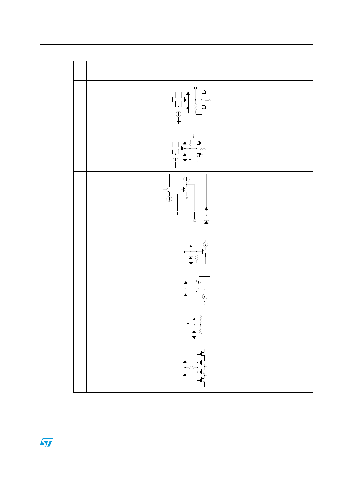
Table 2. Pin description
Pin Name
32 GND_LNA GND Low Noise Amplifier ground
I/O
type
I/O schematic Description
Vcc
IN_LNA
Vcc
GND_LNA
1 IN_LNA I Low Noise Amplifier input
2 Vcc_LNA Vcc
Low Noise Amplifier
supply voltage
3 Vcc_Div Vcc Divider supply voltage
4 Vcc_XTAL Vcc Crystal supply voltage
Vcc
Vcc
5XTAL2 O 2nd Crystal input
6XTAL1 I 1
XTAL2
Vcc
XTAL1
Vcc
Vcc
st
Crystal input
Vcc
7 CK_OUT O Clock output
CK_OUT
Vcc
Vcc
LPF
8 LPF I/O Loop filter
9 Vcc_VCO Vcc VCO supply voltage
Vcc
10 EN_XTAL I Crystal oscillator enable
EN_Xtal
11 NC Not connected
7/35
Block diagram and pin configuration STB5701
Table 2. Pin description (continued)
Pin Name
12 SCL I I2C clock
I/O
type
I/O schematic Description
Vcc
Vcc
SCL
Vcc
13 SDA I I2C data In/Out
SDA
14 STATE O High when selecting UHF
Vcc
Vcc
STATE
Vcc
Vcc
15 IR_IN I From external IR source
IR_IN
16 Vcc_Dig Vcc Digital section supply voltage
Vcc
17 DOUT O Digital serial output
18 NotReset I Global reset, active low
notReset
DOUT
Vcc
Vcc
8/35
STB5701 Block diagram and pin configuration
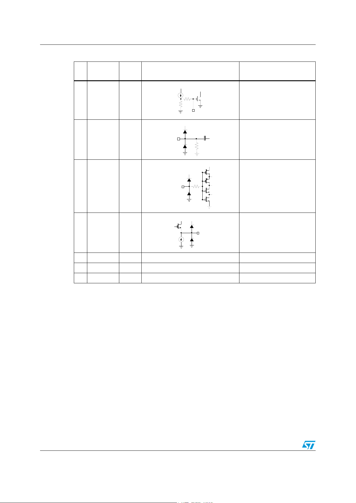
Table 2. Pin description (continued)
Pin Name
I/O
type
I/O schematic Description
PK2 Vcc
Vcc
19 PK2 I/O Max. peak detector
Vcc
Vcc
20 PK1 I/O Min. peak detector
PK1
21
FSK_Discrim
I/O FSK discriminator
FSK_Discr
Vcc
Vcc
22
Chan_Filter3
Chan_Filter2
23
Chan_Filter1
24
I/O Channel filter
I/O Channel filter
I/O Channel filter
25 SAD I I2C address selection
Chan_Filter3
Chan_Filter2
SAD
Chan_Filter1
Vcc
Vcc
Vcc
Vcc
Vcc
Vcc
9/35
Block diagram and pin configuration STB5701
Table 2. Pin description (continued)
Pin Name
26 RSSI_OUT O
27 IF2 I External IF filter input
28 Test_EN I Test mode enable
29 IF1 O External IF filter output
I/O
type
I/O schematic Description
Vcc
Radio strength signal
indicator output
RSSI_OUT
Vcc
IF2
Vcc
Vcc
TEST_EN
VccVcc
IF1
30 Vcc_IF Vcc IF supply voltage
31 Vcc_MIX Vcc Mixer supply voltage
EP GND GND Ground
10/35
STB5701 Block diagram and pin configuration
Figure 2. Test circuit
GND
1
2
EN_XTAL
SCL
NC
SDA
11/35

Block diagram and pin configuration STB5701
Table 3. Bill of material
Component Size Manufacturer Part number Description
C1 0603 MURATA Series GRM39 LNA Input matching
C2 0603 MURATA Series GRM39 Crystal load capacitor
C3 0603 MURATA Series GRM39 Crystal load capacitor
C4 0603 MURATA Series GRM39 Loop filter capacitor
C5 0603 MURATA Series GRM39 Loop filter capacitor
C6 0603 MURATA Series GRM39 Peak detector capacitor
C7 0603 MURATA Series GRM39 Peak detector capacitor
C8 0603 MURATA Series GRM39 FSK Discriminator Tuning
C9 0603 MURATA Series GRM39 Channel filter capacitor
C10 0603 MURATA Series GRM39 Channel filter capacitor
C11 0603 MURATA Series GRM39 RSSI output low path capacitor
C12 0603 MURATA Series GRM39 IF Filter DC Block
C13 0603 MURATA Series GRM39 IF Filter DC Block
R1 0603 NEOHM Series CRG0603 Resistor load capacitor
R2 0603 NEOHM Series CRG0603 Loop filter resistor
R3 0603 NEOHM Series CRG0603 Peak detector resistor
R4 0603 NEOHM Series CRG0603 Peak detector resistor
R5 0603 NEOHM Series CRG0603 RSSI output resistor
R6 0603 NEOHM Series CRG0603 IF Filter Matching
R7 0603 NEOHM Series CRG0603 IF Filter Matching
L1 0603 MURATA LQP18M LNA input matching
X1 CS10 CITIZEN
CS10-
27.000MABJTR
Crystal
F1 Toko SK107M2N-A0-20X Ceramic filter
F2 Toko CDF107F-AO-022 Ceramic resonator
12/35

STB5701 Electrical specifications
2 Electrical specifications
2.1 Absolute maximum ratings
Stressing the device above the rating listed in the “Absolute maximum ratings” table may
cause permanent damage to the device. These are stress ratings only and operation of the
device at these or any other conditions above those indicated in the Operating sections of
this specification is not implied. Exposure to Absolute Maximum Rating conditions for
extended periods may affect device reliability. Refer also to the STMicroelectronics SURE
Program and other relevant quality document
Table 4. Absolute maximum ratings (T
Symbol Parameter Value Unit
V
CC
T
T
stg
Supply voltage 4.5 V
Junction temperature -40 to 150
j
Storage temperature -55 to + 150
2.2 Thermal data
Table 5. Thermal data
Symbol Parameter Value Unit
T
a
θ
th
Operating temperature 0 + 70
Thermal resistance junction to ambient 40
amb
= 25oC)
o
o
o
o
C/W
C
C
C
13/35

Electrical characteristics STB5701
3 Electrical characteristics
(VCC = 3.3 V, Zs = 50 Ω, Ta = 25 oC, unless otherwise specified).
Table 6. Electrical characteristics
Symbol Parameters Test conditions Min. Typ. Max. Unit
Vcc Supply voltage 2.7 3.3 3.6 V
f
rx
Receive
frequency range
350 400 MHz
∆f
FSK frequency
deviation
25 37.5 50 kHz
FSK receive
I
rx_FSK
current
High gain LNA 25 mA
consumption
En_Xtal
5
20
I
cc_standby
Standby current
consumption
RF Enable
bit=0
(PIN 10) high /
floating
En_Xtal (PIN 10)
low
FSK data rate (Manchester encoding) 2 10 kbps
RLin Input return loss 10 dB
Max RF power
input
=369.5MHz
RF
1
= 371.1MHz
RF
2 kbps
manchester
encoding
P
Input sensitivity
min
BER ≤ 10
-3
BW = 300KHz
FSK 37.5 KHz
deviation
Channel
blocking
(1)
+/-1MHz
+/-6MHz
2
RF3 = 375.3MHz
= 376.9MHz
RF
4
= 388.3MHz
RF
5
-109 dBm
RF6 = 391.5MHz
= 394.3MHz
RF
7
= 395.9MHz
RF
8
+/-30KHz -103 dBm
RF
X
50
50
0dBm
Image Rejection 35 dB
mA
µA
dBc
dBc
I2C I/O pins
V
IH
V
IL
Input logic
voltage high
Input logic
voltage low
14/35
0.7 Vcc
-0.5
3.6 V
0.3Vcc
V

STB5701 Electrical characteristics
Table 6. Electrical characteristics (continued)
Symbol Parameters Test conditions Min. Typ. Max. Unit
V
OL
Output logic
voltage low
Hysteresis of
V
HYST
schmitt trigger
for inputs
Output fall time
from V
IHmin
with a
V
t
of
ILmax
bus capacitance
from 10pF to
400pF
Input current
each I/O pin with
I
an input voltage
i
between 0.1V
and 0.9V
Capacitance for
C
i
each I/O pin
C
Capacitive load
b
for each bus line
I2C Standard mode
f
SCL
t
SU_STA
t
HD_STA
t
HIGH
t
LOW
t
SU_DAT
t
HD_DAT
t
R
t
F
SCL clock
frequency
Setup time for
START condition
Hold time for
START condition
SCL high time 4 µs
SCL low time 4.7 µs
DATA setup time 250 ns
DATA hold time 0 3.45 µs
SDA, SCL rise
time
SDA, SCL fall
time
cc
to
cc
0.4 V
0.05 Vcc V
20+ 0.1C
b
250 ns
-10 10 µA
10 pF
400 pF
0 100 kHz
4.7 µs
4µs
1000 ns
300 ns
t
SU_STO
t
BUF
Setup time for
STOP condition
Bus free time
between STOP
and START
condition
4µs
4.7 µs
15/35

Electrical characteristics STB5701
Table 6. Electrical characteristics (continued)
Symbol Parameters Test conditions Min. Typ. Max. Unit
I2C Fast mode
f
SCL
t
SU_STA
t
HD_STA
t
HIGH
t
LOW
t
SU_DAT
t
HD_DAT
t
R
t
F
t
SU_STO
SCL clock
frequency
Setup time for
START condition
Hold time for
START condition
0 400 kHz
0.6 µs
0.6 µs
SCL high time 0.6 µs
SCL low time 1.3 µs
DATA setup time 100 ns
DATA hold time 0 0.9 µs
SDA, SCL rise
time
SDA, SCL fall
time
Setup time for
STOP condition
0.6 µs
300 ns
300 ns
Bus free time
t
BUF
between STOP
and START
1.3 µs
condition
1. Desired signal 10dB above the input sensitivity level, CW interferer power level increased until BER ≤10
-3
16/35

STB5701 Functional description
4 Functional description
4.1 General description
The STB5701 FSK/ASK receiver is a heterodyne configuration (10.7 MHz IF Frequency)
and it is designed for applications in the 350MHz to 400MHz frequency range and includes
ASK and FSK detectors. The synthesizer has a typical channel spacing of better than 100
kHz and uses a integrated fully VCO. With the STB5701 receiver chip, various circuit
configurations can be arranged in order to meet a number of different customer
requirement.
The STB5701 is housed in a VQF package 5mm x 5mm 32 leads.
The STB5701 receiver IC consists of the following building blocks:
● Phase Locked Loop Synthesizer (PLL): M-Counter, A-Counter, Prescaler, Phase-
Frequency Detector (PFD), Charge Pump (CP), Voltage Controlled Oscillator (VCO).
● Programmable reference divider for crystal and channel step selection.
● Low Noise Amplifier (LNA) with AGC function for high sensitivity and dynamic range RF
signal reception.
● Image Rejection Mixer for down conversion of the RF signal to the IF (without external
saw image filter).
● IF amplifier to amplify and limit the IF signal and for RSSI generation.
● Phase coincidence demodulator to demodulate the IF signal.
● Operation amplifier for data slicing, filtering and ASK detection.
● Min/max peak detector to create a DC output voltage equal to the mean of the min and
max peak value of the data signal.
● I2C bus to exchange data between the STB5701 and the micro.
● Start code detector (SCD) to recognize a valid data signal to prevent continuos toggling
of data in the absence of an RF Signal due to the noise.
● Bias circuitry for band gap biasing and circuit shutdown.
17/35

Functional description STB5701
r
P
O
O
N
R
4.2 Programmable Phase Locked Loop synthesizer (PLL)
Figure 3. PLL block diagram
(3) VCC_Div
(4) VCC_XTAL
(5) XTAL2
(6) XTAL1
CK_OUT
(7)
(8) LF
Pierce
Crystal
Oscillator
Clk
f
XTAL
(CLKOUT_ENABLE)
Image Rejection Mixer
(PLL_A, PLL_M)
1 N
1 R
(PLL_R)
I2C
VCC_VCO
(9)
f
VC
EN_Xtal
10
VCO
: 2
TANK
2 f
VC
NC
(11)
I2C
PLL
Synthetize
f
PFD
C
f
I2C
The synthesized programmable local oscillator is a Phase Locked Loop (PLL) using a
'parallel-resonant' quartz crystal as frequency reference. The PLL block contains a phase
detector, charge pump, VCO, Programmable N and R Divider and a Crystal Oscillator. The
synthesized frequency (fVCO) is set by programming the 'N' Divider through the I2C
interface (PINs 12, 13).
f
f
VCO
= f
R
= N . fN = N
/ R
XTAL
.
fR = (N / R)
4.2.1 Divider (a-counter, m-counter and prescaler)
The main divider (N) of the PLL contains a 3-bit A-counter, a 10-bit M-counter and an 8/9
prescaler. The divider ratio of the prescaler is controlled by the program counter and the
swallow counter. During one cycle, the prescaler divides by 9 until the swallow A-counter
reaches its terminal count. Afterwards the prescaler divider by 8 until the program counter
reaches its terminal count. Therefore the overall feedback divider ratio can be expressed as:
.
N = 9
A + 8 . (M - A)
18/35
.
f
XTAL

STB5701 Functional description
The A-counter configuration represents the lower bits in the feedback divider register and
the upper bits the M-counter configuration respectively. According to that, the following
counter ranges are implemented:
≤ A ≤ 7
0
7
≤ M ≤ 1023
and therefore the range of the overall feedback divider ratio results in:
≤ N ≤ 8191
56
The user does not need to care about the A- and M-counter settings. It is only necessary to
know the overall feedback divider ratio N to program the register settings.
4.2.2 Reference divider
The reference divider reduces the frequency of the external crystal (FXTAL) to an internal
reference frequency (FR) used for the phase-locked loop.
This value, corresponding to the channel step, it is set by programming a 10-bit counter
through the I2C interface (PINs 12, 13).
Therefore the range of the Reference divider ratio is:
4.2.3 Phase Frequency Detector
The phase detector (PFD) is a device that compares two input (fN and fR) phases,
generating an output that is a measure of their phase difference.
The gain of the phase detector can be expressed as:
where ICP is the charge pump current.
0
≤ R ≤ 1023
K
= ICP / 2π
PD
If fR doesn't equal fN, the phase-error signal, after being filtered and amplified, causes the
VCO frequency to deviate in the direction of fR.
19/35

Functional description STB5701
I
I
r
4.2.4 Loop filter
An external PLL loop filter is connected to pin LF (PIN 8). The loop filter controls the
dynamic behavior of the PLL, primarily lock time and reference spur levels. Generally, the
PLL lock time is a small fraction of the overall receiver start-up time. The crystal oscillator is
the largest contributor to start-up time.
4.3 Receiver section
The integrated receiver is intended to be used as a single-conversion FSK/ASK receiver. It
consists of a low noise amplifier, mixer, IF filter, limiter, FSK demodulator, a LPF amplifier,
and a data slicer. The received strength signal indicator (RSSI) can be used for fast carrier
sense detection or as amplitude shift keying, (ASK) demodulator.
4.3.1 Low Noise Amplifier (LNA)
Figure 4. LNA block diagram
32
GND_LNA
(1) IN_LNA
(2) VCC_LNA
(LNA_GAIN)
Delay
Clk
mage RejectionMixe
I2C
RSS
Threshold
The LNA is based on a cascode topology for low-noise, high gain and good reverse
isolation. The LNA output is directly connected to the mixer removing the external output
matching.
It has 2 step gain managed by an internal AGC. This AGC circuit monitors the RSSI output.
The AGC has a hysteresis of ~10dB.
20/35

STB5701 Functional description
p
4.3.2 Image Rejection Mixer
Figure 5. Mixer block diagram
(31)
Vcc_MIX
s
LNA
RFAm
Image Rejection Mixer
VCO
An excellent feature of the STB5701 is the integrated image rejection mixer. This device
was designed to eliminate the need for a costly front-end SAW filter for many applications.
The advantage of not using a SAW filter is increased sensitivity, simplified antenna
matching, less board space, and lower cost.The mixer cell is a pair of double-balanced
mixers that perform an IQ down conversion of the 350-400MHz RF input to the IF
(10.7MHz) with low-side injection (i.e., f
= fLO - fIF). The Image Rejection circuit combines
RF
these signals to achieve ~35dB of Image Rejection over the full temperature range.
Low-side injection is required due to the on-chip Image Rejection architecture.
4.3.3 ASK/FSK demodulator and data filter
The received signal strength indicator (RSSI) voltage is proportional to the log of the downconverted RF signal at the IF limiting amplifier input. It also used as demodulator for
amplitude-shift \ keying (ASK) modulation. The signal coming from the RSSI amplifier is
converted into the raw data signal by the ASK/FSK demodulator. The ASK or FSK
modulation selection is set by I2C interface.
IF Filter
s
I2C
(SC_FILTER)
The dynamic range of the RSSI amplifier is exceeded if the RF input signal is about 80
dB higher compared to the RF input signal at full sensitivity.
In FSK mode, the S/N ratio is not affected by the dynamic range of the RSSI amplifier but at
FSK receive mode the RSSI output provides a field strength indication.
Coming from the RSSI the FSK signal is fed to the input of the FSK demodulator. After
buffering the signal is fed to a phase discriminator. The phase shift is generated by
an external 10.7MHz Ceramic discriminator connected to FSK_Discr. (PIN 21).
The FSK demodulator is intended to be used for an FSK deviation of 37.5 kHz. Lower values
may be used but the sensitivity of the receiver is reduced in that condition. After
demodulation a 2nd order Sallen and Key filter is provided in order to suppress unwanted
frequency components.
21/35

Functional description STB5701
FSK
R
D
D
R
ccVcc
Figure 6. ASK/FSK demodulator block diagram
FSK_Discr
Pin 21
SCD
SSI
SSI
I2C
(ASK_NOTFSK)
ata Slicer
ASK
FSK
Demodulator
Mean
Peak
etector
Min
Max
Chan_Filter1 (24)
Chan_Filter2 (23)
Chan_Filter3 (22)
FSK_Discr
(21)
10.7 MHz
Discriminator
(20)
PK1
PK2
(19)
notReset 18
V
22/35

STB5701 Functional description
D
r
4.3.4 Min /Max peak detector
The peak detector embedded in the STB5701, in conjunction with an external RC filter
(PINs 22, 23, 24), generates a DC output voltage equal to the mean of the min and max
peak value of the data signal. The resistor provides a path for the capacitor to discharge,
allowing the peak detector to dynamically follow peak changes of the data filter output
voltage.
4.3.5 Data slicer
The purpose of the data slicer is to take the analog output of the data filter and convert it to
a digital signal. This is achieved by using a comparator and comparing the analog input to a
threshold voltage. One input is supplied by the data filter output.
The other path is fed to the min/max Peak detector to derive the average value (DC
component) as an adaptive slice reference which is presented to the positive comparator
input. The adaptive reference allows detecting the received data over a large range of noise
floor levels.
4.4 Digital control and source selection
Figure 7. Digital section block diagram
Test_EN
Pin 28
STATE
(14)
SAD
Pin 25
SCD
IR_IN
(15)
ata Slice
Vcc_Dig
(16)
notReset
DOUT (17)
18
SCL
(12)
Clk
Digital
Section
I2C
Interface
SDA
(13)
The STB5701 digital section is responsible for the following functions:
● Configuration of the RF front end through software programmable config bits.
● Configuration of the PLL through software programmable registers (PLLA,M,R).
● Detection of a pre-programmed start code sequence (one of two possibilities).
● Arbitration between UHF and IR sources.
The serial data emerges from the DATA output pin (PIN 17) and the system state emerges
from the STATE output pin (PIN 14).
23/35

Functional description STB5701
4.4.1 State pin
The STATE output pin may be configured in one of two ways:
● To reflect the state of the start code detection block officiated = detected, 0 = searching
or off), the state can be cleared by a programmable time out or a software reset.
● To operate as a true interrupt with associate status bit and a software clearing
mechanism.
The state output may be optionally inverted.
4.4.2 Data pin
The DATA output pin is driven by one of two sources:
● The IR_IN pin.
● The UHF input from the RF front end.
4.4.3 MODE register
The DATA source selected at any time is governed by the MODE register, the options are as
follows:
● IR_IN only, direct connection.
● UHF only, direct connection.
● IR triggered, the output is zero and switched to UHf on detection of a valid start code.
● IR/UHF arbitrated, the output comes by default from IR_IN, however on detection of a
valid start code the output is switched to select the UHF source. The switch back to IR
is accomplished in one of two ways.
A software reset is programmed.
The time-out counter has been set and has timed out.
24/35

STB5701 Functional description
4.5 Start code detection example
This section explains the operation of the start code detector with reference to the start code
sequence illustrated in the following figure:
Figure 8. START code
1112
1 ms
910
2 ms
6
78
5
1 ms
34
2
2 ms
0
1
500 µs
Firstly we assume the nominal symbol duration is 500
13 symbol (denoted as 12 to 0 in the figure above).
If the device is operating from a 27 Mhz external clock then we program the prescaler to 27.
The internal sampling clock will be 1Mhz and the sampling resolution will be 1us. To add
some error tolerance we also program an upper and lower bound on the symbol duration as
well as the nominal value. In this case 400 (corresponding to 400us) in
SCD_symbol_min_time register, 500 (corresponding to 500us) in SCD_symbol_nom_time
and 600 (corresponding to 600us) in SCD_symbol_max_time.
µs, in this example there are then
Now we program 0b1001111001111 into the SCD_code register and 13 (0x0d)
corresponding to 13 symbols to be detected into the SCD_code_length register. The start
code detection is started by setting the enable and research bits in SCD_config register to
‘1’.
The start code detector checks for the minimum symbol time of each symbol and the
sequence in which symbols are received. If the symbol time is not respected by the input
(incase of noise) the start code detection is re-initialized.
The detector is capable of simultaneously searching for two different start codes, the
alternative code is written into the upper 16 bits of SCD_code register.
25/35

Functional description STB5701
4.6 Registers list
Two unique I2C addresses have been reserved for the STB5701 device, the appropriate one
is selected using the SAD input pin.
Table 7. I2C reserved addresses
SAD Address
0 0110010x
1 (spare) 0110011x
4.7 Register summary
The I2C mapped address space of the STB5701 is given below:
Table 8. I2C address breakdown
Base address Group Description
0x00 Top Level See table 9 below
0x80 SCD Block See table 10 below
Table 9. I2C mapped top level registers - summary
Address Name Reset value Function
0x00 DIG_config 0x00000000 Digital configuration
0x04 RF_config 0x00000000 Configure RF front end
0x08 PLL_A 0x00000000 PLL post divider
0x0C PLL_M 0x00000000 PLL feedback divider
0x10 PLL_R 0x00000000 PLL reference divider
Unique to this device.
Table 10. I2C mapped SCD registers - summary
Address Name Reset value Function
0x80 Scd_config 0x00000000 SCD configuration register.
0x84 Scd_status 0x00000000 SCD status can be read from this register.
0x88 Scd_code 0x00000000 Expected Start code is stored in this register.
0x8C Scd_code_length 0x00000000
0x90 Scd_symbol_min_time 0x00000000
0x94 Scd_symbol_max_time 0x00000000
0x98 Scd_symbol_nom_time 0x00000000 Nominal symbol time is stored in this register.
26/35
Length of the start code is stored in this
register.
Minimum time of the symbol is stored in this
register.
Maximum time of the symbol is stored in this
register.

STB5701 Functional description
Table 10. I2C mapped SCD registers - summary (continued)
Address Name Reset value Function
0x9C Scd_prescaler 0x00000001 Value of prescaler for sampling is stored.
0xA0 Interrupt_enable 0x00000000
0xA4 Interrupt_clear 0x00000000
0xA8 Timeout 0x00000000 Timeout for SCS based on prescaler tick.
4.8 Detailed display description
Table 11. DIG_config register format
DIG_Config 0x00 R/W
Bit Bit field
1:0 MODE 00
2 STATE_SEL 0
3 STATE_INV 0 1: Invert the STATE output
4STATE_DRIVE 0
5 CLKOUT_ENABLE 0 1: Enable clock output buffer
Reset
state
00: UHF direct
01: IR direct
10: UHF triggered (DOUT = 0 when no trigger)
11: IR or UHF triggered
1: STATE is driven by the SCD interrupt output
0: STATE is driven by the SCD detect state
0: Open drain
1: Push pull
Interrupt enable register value is stored in this
register.
Interrupt clear register value is stored in this
register.
Function
31:6 Reserved 0x00 0x00
Table 12. RF_Config register format
RF_Config 0x04 R/W
Bit Bit field
0 RF_ENABLE 0
1ASK_NOTFSK 0
2LNA_GAIN 0
3 Not used 0
31:4 Reserved 0x00 0x00
Reset
state
Function
1: Enable front end
0: Disable front end
1: ASK detection
0: FSK detection
1: Enable AGC
0: Disable AGC (high gain)
27/35

Functional description STB5701
Table 13. PLL_A register
PLL_A 0x08 R/W
Bit Bit field
2:0 PLL_A
31:3 Reserved 0x00 0x00
Reset
state
SAD = 0:
0x1
SAD= 1:
0x7
Function
PLL post divider value.
Reset value determined by level on SAD input.
Table 14. PLL_M register format
PLL_M 0x0C R/W
Bit Bit field Reset state Function
SAD = 0:
9:0 PLL_M
31:10 Reserved 0x00 0x00
0x1D5
SAD= 1:
0x1CD
PLL feedback divider value.
Reset value determined by level on SAD input.
Table 15. PLL_R register format
PLL_R 0x10 R/W
Bit Bit field Reset state Function
9:0 PLL_R 000 PLL reference divider value
31:10 Reserved 0x00 0x00
Table 16. SCD_config register format
SCD_config 0x80 R/W
Bit Bit field Reset state Function
0Enable 0
1 Re-search 0
2 Soft_rst 0 1: Resets all the counters and shift register
3 Reset_shift_reg 0 1: Reset only shift register. Status register is not affected.
31:4 Reserved 0x00 0x00
1: Enables the start code detection circuit
0: By passes SCD, UHF in fed to UHF out
1: Start a fresh research.
Reset automatically to ‘0’ on re-search start
28/35

STB5701 Functional description
Table 17. SCD_status register format
SCD_status 0x84 R
Bit Bit field Reset state Function
0 Detect 0 1: Start code detected, UHF in fed to UHF out
1:2 Reserved 0 00
3 Alternative 0 1: The alternative code was detected
31:4 Reserved 0x00 0x00
Table 18. SCD_code register format
SCD_code 0x88 R/W
Bit Bit field Reset state Function
15:0 Code 0x00 Start code to be detected
31:16 Alt_code 0x00 Alternative start code to be detected
Note: This register holds each start code to be detected.
Table 19. SCD_code_lenth register format
SCD_code_lenth 0x8C R/W
Bit Bit field
4:0 Code_length 0 Length of the start code
15:5 Reserved 0x00 0x00
20:16 Alt_code_length 0 Length of the alternative start code
31:21 Reserved 0x00 0x00
Reset
state
Function
Note: The length of the start code is stored in this register. If the start code length is 10 symbol
then 10 has to be written into this register. Writing 0x00 disables the SCD.
Table 20. SCD_symbol_min_time register format
SCD_symbol_min_time 0x90 R/W
Bit Bit field Reset state Function
15:0 Min_time 0x00 Minimum symbol time
31:16 Reserved 0x00 0x00
Note: The minimum time of the symbol in terms of pre-scaler ticks is stored in this register. If
any symbol violates the minimum symbol time, the SCD process is re-initialized. If a value
0x10 is written into this register, the symbol min. time is 16 pre-scaler clock periods.
29/35

Functional description STB5701
Table 21. SCD_symbol_max_time register format
SCD_symbol_max_time 0x94 R/W
Bit Bit field Reset state Function
15:0 Max_time 0x00 Maximum symbol time
31:16 Reserved 0x00 0x00
Note: The maximum time of the symbol is stored in this register. Any changes in the input data are
allowed only between symbol minimum time and symbol maximum time. The symbol time
counting is done by a clock (enable pulse) which ia output of pre-scaler. If a value 0x10 is
written into this register, the symbol max time is 16 pre-scaler clock periods.
Table 22. SCD_symbol_nom_time register format
SCD_symbol_nom_time 0x98 R/W
Bit Bit field Reset state Function
15:0 Nom_time 0x00 Nominal symbol time
31:16 Reserved 0x00 0x00
Note: The nominal time of the symbol in terms of pre-scaler ticks is stored in this register. This
value is used to register a new symbol when consecutive symbols with same logical value
are received. If a value 0x10 is written into this register, the symbol nominal time is 16 prescaler clock periods.
Table 23. SCD_prescaler register format
SCD_prescaler 0x9C R/W
Bit Bit field Reset state Function
15:0 prescaler 0x01 Pre scaler division value is stored in this register
31:16 Reserved 0x00 0x00
Note: The nominal time of the symbol is stored in this register.
Table 24. Interrupt_enable register format
Interrupt_enable 0xA0 R/W
Bit Bit field Reset state Function
0 scd_detected 0
31:1 Reserved 0x00 0x00
1 Enable interrupt
0 Disable interrupt
Note: The interrupt enable register value is stored in this register.
30/35

STB5701 Functional description
Table 25. Interrupt_clear register format
Interrupt_clear 0xA4 R/W
Bit Bit field Reset state Function
0 scd_clear_int 0
1 Clear interrupt
0 No change on interrupt
31:1 Reserved 0x00 0x00
Note: The interrupt clear register value is stored in this register.
Table 26. Timeout register format
Bitcount 0xA8 R/W
Bit Bit field Reset state Function
23:0 Timeout 0x00 Timeout value, duration is based on prescaler tick.
31:24 Reserved 0x00 0x00
31/35

Package information STB5701
5 Package information
5.1 ECOPACK® packages
In order to meet environmental requirements, ST offers these devices in ECOPACK®
packages. These packages have a Lead-free second-level interconnect. The category of
Second-Level Interconnect is marked on the package and on the inner box label, in
compliance with JEDEC Standard JESD97. The maximum ratings related to soldering
conditions are also marked on the inner box label.
ECOPACK is an ST trademark. ECOPACK specifications are available at: www.st.com.
5.2 QFN32L (5mm x 5mm) information
Figure 9. QFN32L (5mm x 5mm) dimensions
32/35

STB5701 Package information
Table 27. QFN32L (5mm x 5mm) mechanical data
mm
Min. Typ. Max.
A 0.80 0.90 1.00
A1 0.00 0.02 0.05
A3 0.20
b 0.18 0.25 0.30
D 4.85 5.00 5.15
D2 3.50 3.60 3.70
E 4.85 5.00 5.15
E2 3.50 3.60 3.70
e0.50
L 0.30 0.40 0.50
ddd 0.05
33/35

Revision history STB5701
6 Revision history
Table 28. Document revision history
Date Revision Changes
01-Oct-2007 1 Initial release.
34/35

STB5701
Please Read Carefully:
Information in this document is provided solely in connection with ST products. STMicroelectronics NV and its subsidiaries (“ST”) reserve the
right to make changes, corrections, modifications or improvements, to this document, and the products and services described herein at any
time, without notice.
All ST products are sold pursuant to ST’s terms and conditions of sale.
Purchasers are solely responsible for the choice, selection and use of the ST products and services described herein, and ST assumes no
liability whatsoever relating to the choice, selection or use of the ST products and services described herein.
No license, express or implied, by estoppel or otherwise, to any intellectual property rights is granted under this document. If any part of this
document refers to any third party products or services it shall not be deemed a license grant by ST for the use of such third party products
or services, or any intellectual property contained therein or considered as a warranty covering the use in any manner whatsoever of such
third party products or services or any intellectual property contained therein.
UNLESS OTHERWISE SET FORTH IN ST’S TERMS AND CONDITIONS OF SALE ST DISCLAIMS ANY EXPRESS OR IMPLIED
WARRANTY WITH RESPECT TO THE USE AND/OR SALE OF ST PRODUCTS INCLUDING WITHOUT LIMITATION IMPLIED
WARRANTIES OF MERCHANTABILITY, FITNESS FOR A PARTICULAR PURPOSE (AND THEIR EQUIVALENTS UNDER THE LAWS
OF ANY JURISDICTION), OR INFRINGEMENT OF ANY PATENT, COPYRIGHT OR OTHER INTELLECTUAL PROPERTY RIGHT.
UNLESS EXPRESSLY APPROVED IN WRITING BY AN AUTHORIZED ST REPRESENTATIVE, ST PRODUCTS ARE NOT
RECOMMENDED, AUTHORIZED OR WARRANTED FOR USE IN MILITARY, AIR CRAFT, SPACE, LIFE SAVING, OR LIFE SUSTAINING
APPLICATIONS, NOR IN PRODUCTS OR SYSTEMS WHERE FAILURE OR MALFUNCTION MAY RESULT IN PERSONAL INJURY,
DEATH, OR SEVERE PROPERTY OR ENVIRONMENTAL DAMAGE. ST PRODUCTS WHICH ARE NOT SPECIFIED AS "AUTOMOTIVE
GRADE" MAY ONLY BE USED IN AUTOMOTIVE APPLICATIONS AT USER’S OWN RISK.
Resale of ST products with provisions different from the statements and/or technical features set forth in this document shall immediately void
any warranty granted by ST for the ST product or service described herein and shall not create or extend in any manner whatsoever, any
liability of ST.
ST and the ST logo are trademarks or registered trademarks of ST in various countries.
Information in this document supersedes and replaces all information previously supplied.
The ST logo is a registered trademark of STMicroelectronics. All other names are the property of their respective owners.
© 2007 STMicroelectronics - All rights reserved
STMicroelectronics group of companies
Australia - Belgium - Brazil - Canada - China - Czech Republic - Finland - France - Germany - Hong Kong - India - Israel - Italy - Japan -
Malaysia - Malta - Morocco - Singapore - Spain - Sweden - Switzerland - United Kingdom - United States of America
www.st.com
35/35
 Loading...