

查询P4NK60ZFP供应商
STP4NK60Z-STP4NK60ZFP-STB4NK60Z-1
N-CHANNEL600V-1.76Ω-4ATO-220/FP/DPAK/IPAK/D2PAK/I2PAK
STB4NK60Z-STD4NK60Z-STD4NK60Z-1
Zener-Protected SuperMESH™Power MOSFET
TYPE V
STP4NK60Z
STP4NK60ZFP
STB4NK60Z
STB4NK60Z-1
STD4NK60Z
STD4NK60Z-1
■ TYPICAL R
■ EXTREMELY HIGHdv/dt CAPABILITY
■ 100% AVALANCHE TESTED
■ GATE CHARGE MINIMIZED
■ VERY LOW INTRINSICCAPACITANCES
■ VERY GOOD MANUFACTURING
600 V
600 V
600 V
600 V
600 V
600 V
(on) = 1.76 Ω
DS
DSS
R
DS(on)
<2Ω
<2Ω
<2Ω
<2 Ω
<2Ω
<2Ω
I
D
4A
4A
4A
4A
4A
4A
Pw
70 W
25 W
70 W
70 W
70 W
70 W
REPEATIBILITY
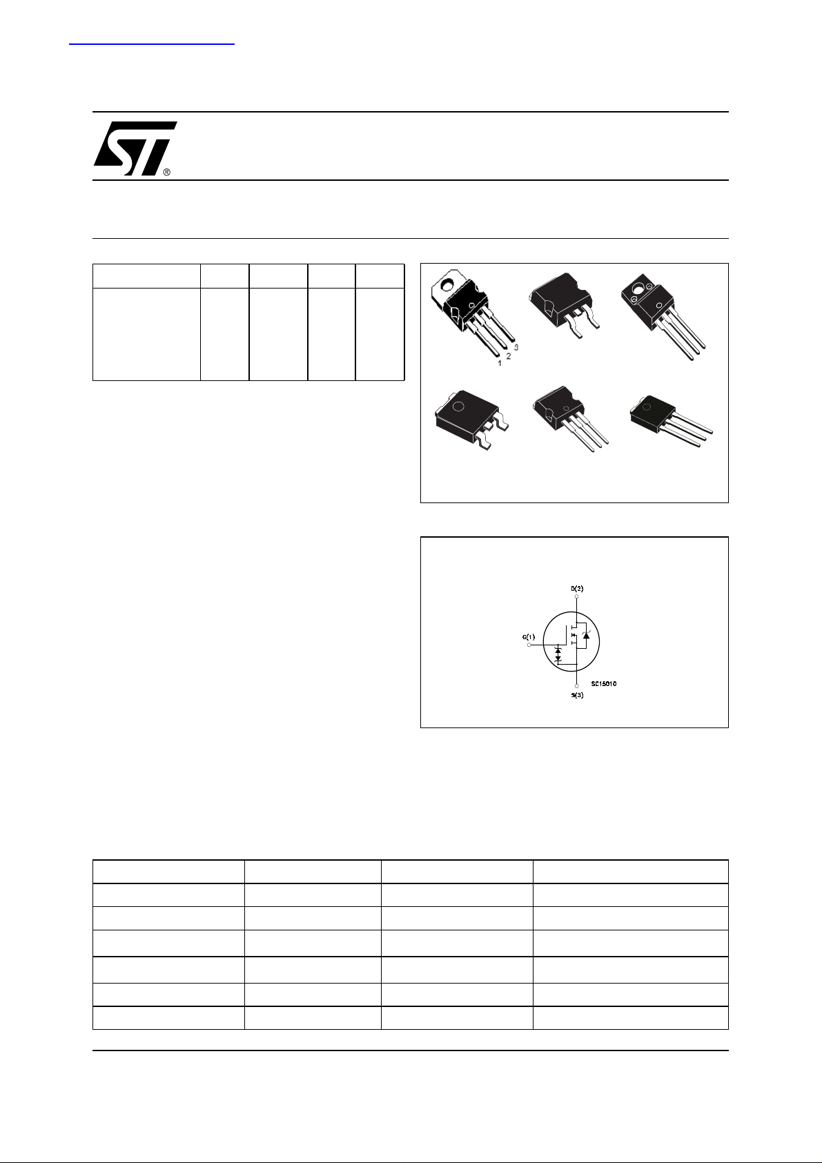
DESCRIPTION
The SuperMESH™ series is obtained through an
extreme optimization of ST’s well established stripbased PowerMESH™ layout. In addition to pushing
on-resistance significantly down, special careis taken to ensure a very good dv/dt capability for the
most demanding app lications. Such series complements S T full range of high voltage MOSFETs including revolutionary MDm es h™ products.
3
1
D2PAK
TO-220
DPAK
3
1
2
1
I2PAK
TO-220FP
3
INTERNAL SCHEMATIC DIAGRAM
IPAK
3
2
1
3
2
1
APPLICATIONS
■ HIGH CURRENT, HIGH SPEED SWITCHING
■ IDEAL FOR OFF-LINE POWER SUPPLIES,
ADAPTORS AND PFC
■ LIGHTING
ORDERING INFORMATION
SALES TYPE MARKING PACKAGE PACKAGING
STP4NK60Z P4NK60Z TO-220 TUBE
STP4NK60ZFP P4NK60ZFP TO-220FP TUBE
STB4NK60ZT4 B4NK60Z
STB4NK60Z-1 B4NK60Z
STD4NK60ZT4 D4NK60Z DPAK TAPE & REEL
STD4NK60Z-1 D4NK60Z IPAK TUBE
2
PAK
D
I2PAK
TAPE & REEL
TUBE
1/16March 2003
STP4NK60Z,STP4NK60ZFP,STB 4N K60Z,STB4NK60Z-1,STD4NK60Z,STD4N K 60Z-1
ABSOLUTE MAXIMUM RATINGS
Symbol Parameter Value Unit
STP4NK60Z
I
V
DM
P
V
DGR
V
I
I
TOT
DS
GS
D
D
STB4NK60Z
STB4NK60Z-1
Drain-source Voltage (VGS=0)
Drain-gate Voltage (RGS=20kΩ)
Gate- source Voltage ± 30 V
Drain Current (continuous) at TC= 25°C
Drain Current (continuous) at TC= 100°C
()
Drain Current (pulsed) 16 16 (*) 16 A
Total Dissipation at TC= 25°C
4 4 (*) 4 A
2.5 2.5 (*) 2.5 A
70 25 70 W
STP4NK60ZFP
600 V
600 V
Derating Factor 0.56 0.2 0.56 W/°C
V
ESD(G-S)
Gate source ESD(HBM-C=100pF, R=1.5KΩ) 3000 V
dv/dt (1) Peak Diode Recovery voltage slope 4.5 V/ns
V
ISO
T
j
T
stg
() Pulse width limited by safe operating area
(1) I
≤4A, di/dt ≤200A/µs, VDD≤ V
SD
(*) Limited only by maximum temperature allowed
Insulation Withstand Voltage (DC) - 2500 - V
Operating Junction Temperature
Storage Temperature
(BR)DSS,Tj≤TJMAX.
-55 to 150
-55 to 150
STD4NK60Z
STD4NK60Z-1
°C
°C
THERMAL DATA
TO-220
D
2
I
2
PAK
PAK
TO-220FP
Rthj-case Thermal Resistance Junction-case Max 1.78 5 1.78 °C/W
Rthj-amb Thermal Resistance Junction-ambient Max 62.5 100 °C/W
T
l
Maximum Lead Temperature For Soldering Purpose
300 °C
DPAK
IPAK
AVALANCHE CHARACTERISTICS
Symbol Parameter Max Value Unit
I
AR
Avalanche Current, Repetitive or Not-Repetitive
(pulse width limited by T
E
AS
Single Pulse Avalanche Energy
(starting T
max)
j
= 25 °C, ID=IAR,VDD=50V)
j
4A
120 mJ
GATE-SOURCE ZENER DIODE
Symbol Parameter Test Conditions Min. Typ. Max. Unit
BV
GSO
Gate-Source Breakdown
Voltage
Igs=± 1mA (Open Drain) 30 V
PROTECTION FEATURES OF GATE-TO-SOURCE ZENER DIODES
The built-in back-to-back Zener diodes have specifically been designed to enhance not only the device’s
ESD capability, but also to make them safely absorb possible voltage transients that may occasionally be
applied from gate to source. In this respect the Zener voltage is appropriate to achie ve an efficient and
cost-effective intervention to protect the device’s integrity. These integrated Zener d iodes thus avoid t he
usage of external components.
2/16
STP4NK60Z,STP4NK60ZFP,STB 4N K60Z,STB4NK60Z-1,STD4NK60Z,STD4N K 60Z-1
ELECTRICAL CHARACTERISTICS (TCASE =25°C UNLESS OT HERWISE SPECIFIED)
ON/OFF
Symbol Parameter Test Conditions Min. Typ. Max. Unit
V
(BR)DSS
Drain-source
Breakdown Voltage
I
DSS
I
GSS
V
GS(th)
R
DS(on)
Zero Gate Voltage
Drain Current (V
GS
=0)
Gate-body Leakage
Current (V
DS
=0)
Gate Threshold Voltage
Static Drain-source On
Resistance
DYNAMIC
Symbol Parameter Test Conditions Min. Typ. Max. Unit
(1) Forward Transconductance VDS=15V,ID=2A 3 S
g
fs
Input Capacitance
Output Capacitance
Reverse Transfer
Capacitance
(3) Equivalent Output
C
oss eq.
C
iss
C
oss
C
rss
Capacitance
SWITCHING ON
Symbol Parameter Test Conditions Min. Typ. Max. Unit
t
d(on)
Q
Q
Q
t
r
g
gs
gd
Turn-on Delay Time
Rise Time
Total Gate Charge
Gate-Source Charge
Gate-Drain Charge
ID=1mA,VGS= 0 600 V
V
= Max Rating
DS
VDS= Max Rating, TC= 125 °C
V
= ± 20V ±10 µA
GS
V
DS=VGS,ID
= 50µA
3 3.75 4.5 V
1
50
VGS=10V,ID= 2 A 1.76 2 Ω
=25V,f=1MHz,VGS= 0 510
V
DS
67
13
VGS=0V,VDS= 0V to 480V 38.5 pF
VDD=300V,ID=2A
RG= 4.7Ω VGS=10V
12
9.5
(Resistive Load see, Figure 3)
=480V,ID=4A,
V
V
DD
GS
=10V
18.8
3.8
26 nC
9.8
µA
µA
pF
pF
pF
ns
ns
nC
nC
SWITCHING OFF
Symbol Parameter Test Conditions Min. Typ. Max. Unit
t
d(off)
Turn-off Delay Time
t
f
Fall Time
VDD= 300 V, ID=2A
R
=4.7ΩVGS=10V
G
29
16.5
(Resistive Load see, Figure 3)
t
r(Voff)
= 480V, ID=4A,
t
f
t
c
Fall Time
Cross-over Time
Off-voltage Rise Time
V
DD
RG=4.7Ω, VGS= 10V
(Inductive Load see, Figure 5)
12
12
19.5
SOURCE DRAIN DIODE
Symbol Parameter Test Conditions Min. Typ. Max. Unit
I
SD
I
SDM
VSD(1)
t
rr
Q
rr
I
RRM
Note: 1. Pulsed: Pulse duration = 300 µs, duty cycle 1.5 %.
2. Pulse width limited by safe operating area.
3. C
Source-drain Current
(2)
Source-drain Current (pulsed)
Forward On Voltage
Reverse Recovery Time
Reverse Recovery Charge
Reverse Recovery Current
is defined as a constant equivalent capacitance giving the same charging time as C
oss eq.
.
V
DSS
ISD= 4 A, VGS=0
I
SD
VDD=24V,Tj= 150°C
(see test circuit, Figure 5)
= 4 A, di/dt = 100A/µs
400
1700
8.5
when VDSincreases from 0 to 80%
oss
4
16
1.6 V
ns
ns
ns
ns
ns
A
A
ns
nC
A
3/16
STP4NK60Z,STP4NK60ZFP,STB 4N K60Z,STB4NK60Z-1,STD4NK60Z,STD4N K 60Z-1
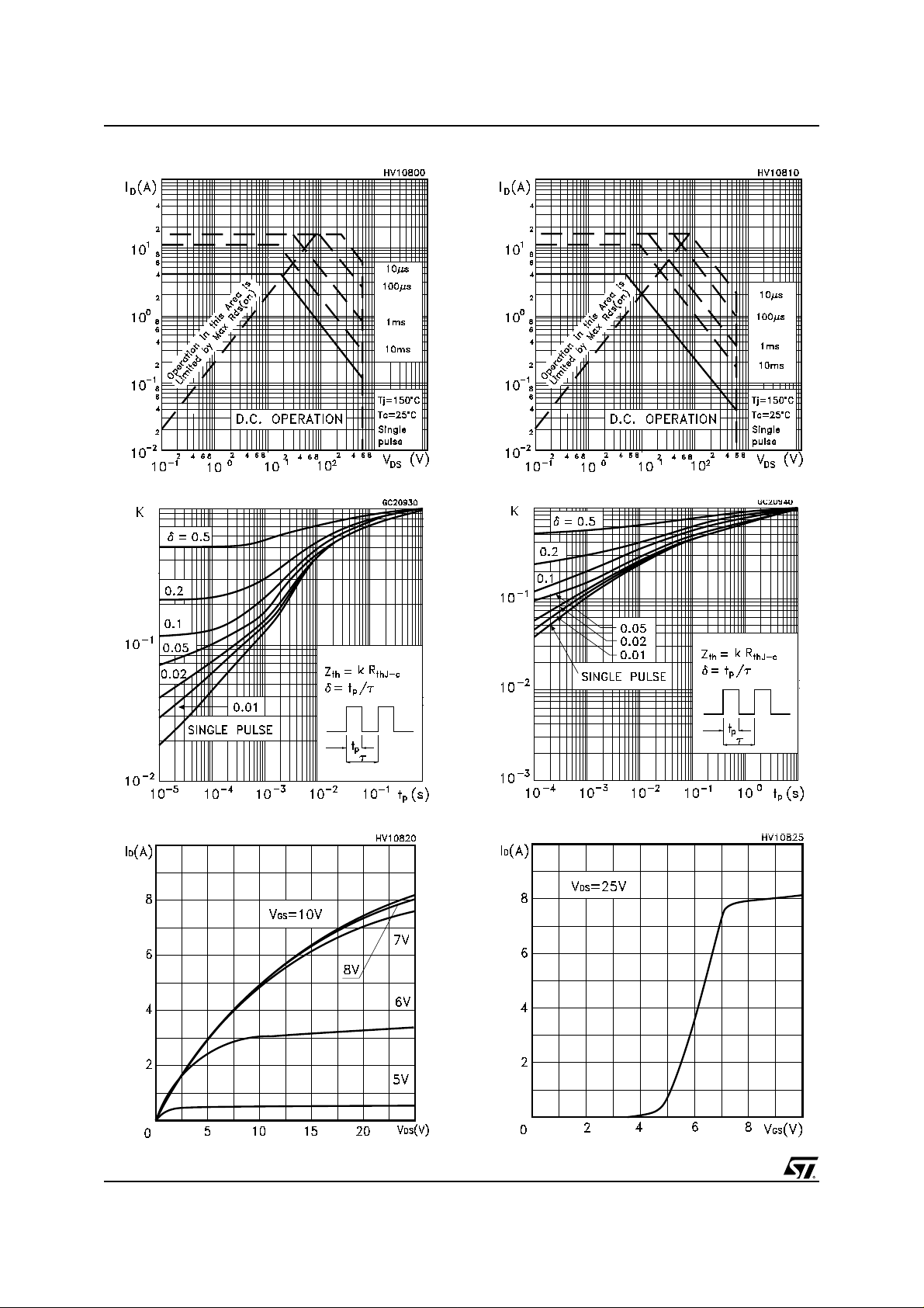
Safe Operating Area For TO-220FPSafeOperatingArea:TO-220/DPA K/IPAK/D2PAK/I2P AK
ThermalImpedance:TO-220/DPAK/IPAK/D2PAK/I2PAKThermal Impedance For TO-220FP
Output Characteristics
4/16
Transfer Characteristics
STP4NK60Z,STP4NK60ZFP,STB 4N K60Z,STB4NK60Z-1,STD4NK60Z,STD4N K 60Z-1
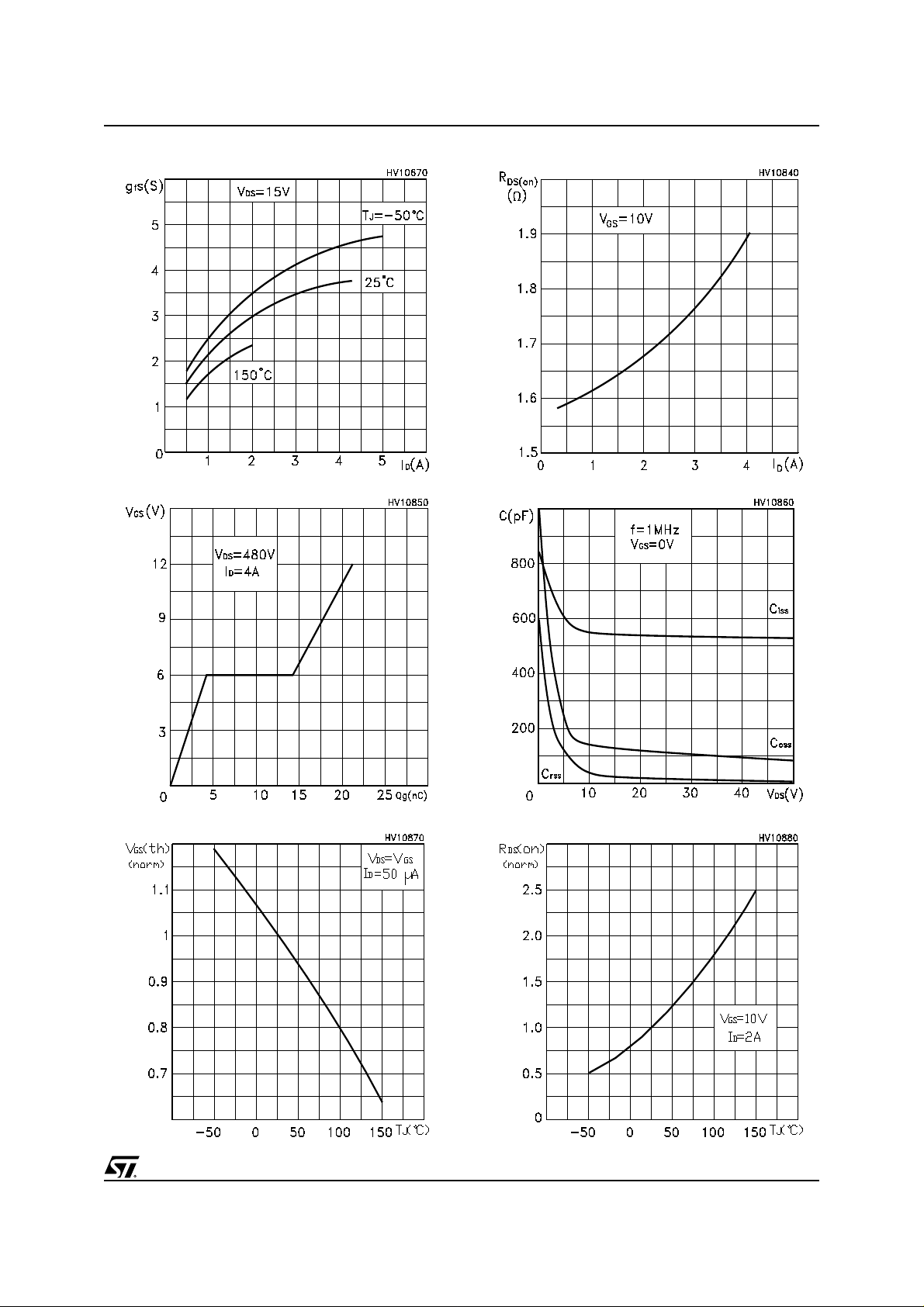
Static Drain-source On ResistanceTransconductance
Gate Charge vs Gate-so urce Voltage Capacitance Variations
Normalized Gate Threshold Voltage vs Temp. Normalized On Resistance vs Temperature
5/16
 Loading...