

查询STB25NM60N供应商
N-CHANNEL 600V 0.140Ω-20A TO-220/FP/D²/I²PAK/TO-247
STP25NM60N - STF25NM60N
STB25N M60N/-1 - STW25NM60N
SECOND GENERATION MDmesh™ MOSFET
PRODUCT PREVIEW
Table 1: Ge neral Features
TYPE V
STB25NM60N-1
STF25NM60N
STP25NM60N
STW25NM60N
STB25NM60N
■ WORLD’S LOWEST ON RESISTANCE
■ TYPICAL R
■ HIGH dv/dt AND AVALANCHE CAPABILITIES
■ 100% AVALANCHE TESTED
■ LOW INPUT CAPACITANCE AND GATE
DS
DSS
(@Tjmax)
650 V
650 V
650 V
650 V
650 V
(on) = 0.140 Ω
R
DS(on)
< 0.170 Ω
< 0.170 Ω
< 0.170 Ω
< 0.170 Ω
< 0.170 Ω
I
D
20 A
20(*) A
20 A
20 A
20 A
CHARGE
■ LOW GATE INPUT RESISTAN CE
DESCRIPTION
The STP25NM60N is realized with the second
generation of MDmesh T echnology. This revolutionary MOSFET associates a new vertical structure to the Company's strip layout to yield the
world's lowest on-resistance and gate charge. It is
therefore suitable for the most demanding high efficiency converters
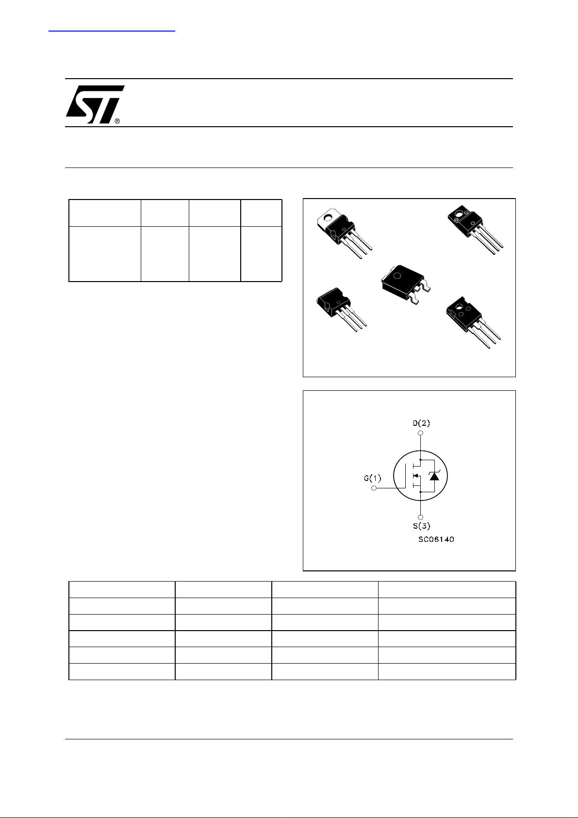
Figure 1: Package
3
2
TO-220
1
TO-220FP
3
1
D²PAK
3
2
1
I²PAK
TO-247
Figure 2: Internal Schematic Diagram
3
2
1
3
2
1
APPLICATIONS
The MDmesh™ II family is very suitable for increase the power density of high voltage converters allowing system miniaturization and higher
efficiencies.
Table 2: Order Code
SALES TYPE MARKING PACKAGE PACKAGING
STB25NM60N-1 B25NM60N I²PAK TUBE
STF25NM60N F25NM60N TO-220FP TUBE
STP25NM60N P25NM60N TO-220 TUBE
STW25NM60N W25NM60N TO-247 TUBE
STB25NM60N B25NM60N D²PAK TAPE & REEL
June 2005
This is prel i m i nary informat i on on a new product now in dev el opment. Details are sub j ect to change w ithout notic e.
Rev. 4
1/12
STP25NM60N - STF25NM60N - STB25NM 60N/-1 - STW25NM60N
Table 3: Absolute Maximum ratings
Symbol Parameter Value Unit
TO-220/I²PAK
TO-247/D²PAK
Drain-source Voltage (VGS = 0) 600 V
Drain-gate Voltage (RGS = 20 kΩ)600V
Gate- source Voltage ± 25 V
Drain Current (continuous) at TC = 25°C
Drain Current (continuous) at TC = 100°C
20 20 (*) A
12.8 12.8 (*) A
Drain Current (pulsed) 80 80 (*) A
Total Dissipation at TC = 25°C
160 40 W
V
I
DM
V
V
P
DS
DGR
GS
I
D
I
D
(1)
TOT
Derating Factor 1.28 0.32 W/°C
dv/dt (2) Peak Diode Recovery voltage slope TBD V/ns
T
stg
T
j
(*) Limited only by maximum temperature allowed
(1) Pulse wi dt h l i m i ted by safe operating area
≤ 20 A, di/dt ≤ 400 A/µ s, VDD =80%V
(2) I
SD
Storage Temperature – 55 to 150 °C
Max. Operating Junction Temperature 150 °C
.
(BR)DSS
Table 4: Thermal Data
TO-220/I²PAK
TO-247/D²PAK
Rthj-case Thermal Resistance Junction-case Max 0.78 3.1 °C/W
Rthj-amb Thermal Resistance Junction-ambient Max 62.5 °C/W
T
l
Maximum Lead Temperature For Soldering Purpose 300 °C
TO-220FP
TO-220FP
Table 5: Avalanche Characteristics
Symbol Parameter Max Value Unit
I
AS
E
AS
Avalanche Current, Repetitive or Not-Repetitive
(pulse width limited by T
max)
j
Single Pulse Avalanche Energy
(starting T
= 25 °C, ID = IAS, VDD = 50 V)
j
ELECTRICAL CHARACTERISTICS (T
=25°C UNLESS OTHERWISE SPECIFIED)
CASE
TBD A
TBD mJ
Table 6: On /Off
Symbol Parameter Test Conditions Value Unit
Min. Typ. Max.
V
(BR)DSS
Drain-source Breakdown
Voltage
dv/dt(2) Drain Source Voltage
Slope
I
DSS
I
GSS
V
GS(th)
R
DS(on
Zero Gate Voltage
Drain Current (V
GS
= 0)
Gate-body Leakage
Current (V
DS
= 0)
Gate Threshold Voltage
Static Drain-source On
Resistance
(2) Characteristic value at turn off on inductive load
ID = 1 mA, VGS = 0 600 V
Vdd=TBD, Id=TBD, Vgs=TBD TBD V/ns
V
= Max Rating
DS
V
= Max Rating, TC = 125°C
DS
V
= ± 20 V 100 nA
GS
V
= VGS, ID = 250 µA 2
DS
3
1
10
4V
VGS = 10 V, ID = 10 A 0.140 0.170 Ω
µA
µA
2/12
STP25NM60N - STF25NM60N - STB25NM 60N/-1 - STW25NM60N
ELECTRICAL CHARACTERISTICS (CONTINUED)
Table 7: Dynamic
Symbol Parameter Test Conditions Min. Typ. Max. Unit
(1) Forward Transconductance VDS = 15V , ID= 10A 17 S
g
fs
C
iss
C
oss
C
rss
C
OSS eq
R
G
t
d(on)
t
r
t
d(off)
t
f
Q
g
Q
gs
Q
gd
Table 8: Source Drain Diode
Symbol Parameter Test Conditions Min. Typ. Max. Unit
I
SD
I
SDM
VSD (1)
t
rr
Q
rr
I
RRM
t
rr
Q
rr
I
RRM
(1) Pulsed: Pulse duration = 300 µs, duty cycl e 1.5 %.
(2) Pulse width limited by safe operating area.
(3) C
oss eq.
Input Capacitance
Output Capacitance
= 25 V, f = 1 MHz,
V
DS
VGS = 0
Reverse Transfer
Capacitance
(3).Equivalent Outpu t
VGS = 0 V, VDS = 0 to 480 V TBD pF
Capacitance
Gate Input Resistance f=1 MHz Gate DC Bias = 0
Test Signal Level = 20mV
Open Drain
Turn-on Delay Time
Rise Time
Turn-off-Delay Time
= 300 V, ID = 10 A,
V
DD
R
= 4.7 Ω, V
G
(see Figure 4)
GS
= 10 V
Fall Time
= 480 V, ID = 20 A,
Total Gate Charge
Gate-Source Charge
Gate-Drain Charge
V
DD
V
= 10 V
GS
(see Figure 7)
Source-drain Current
(2)
Source-drain Current (pulsed)
Forward On Voltage
Reverse Recovery Time
Reverse Recovery Charge
Reverse Recovery Current
Reverse Recovery Time
Reverse Recovery Charge
Reverse Recovery Current
is defined as a constant equivalent capacitance giving the same charging time as C
ISD = 20 A, VGS = 0
= 25 A, di/dt = 100 A/µs
I
SD
VDD = 100V
(see Figure 5)
= 25 A, di/dt = 100 A/µs
I
SD
VDD = 100V, Tj = 150°C
(see Figure 5)
2565
511
77
2 Ω
TBD
TBD
TBD
TBD
93
TBD
TBD
20
80
1.3 V
TBD
TBD
TBD
TBD
TBD
TBD
when VDS increase s from 0 to 80% V
oss
pF
pF
pF
ns
ns
ns
ns
nC
nC
nC
ns
µC
ns
µC
A
A
A
A
DSS
.
3/12
STP25NM60N - STF25NM60N - STB25NM 60N/-1 - STW25NM60N
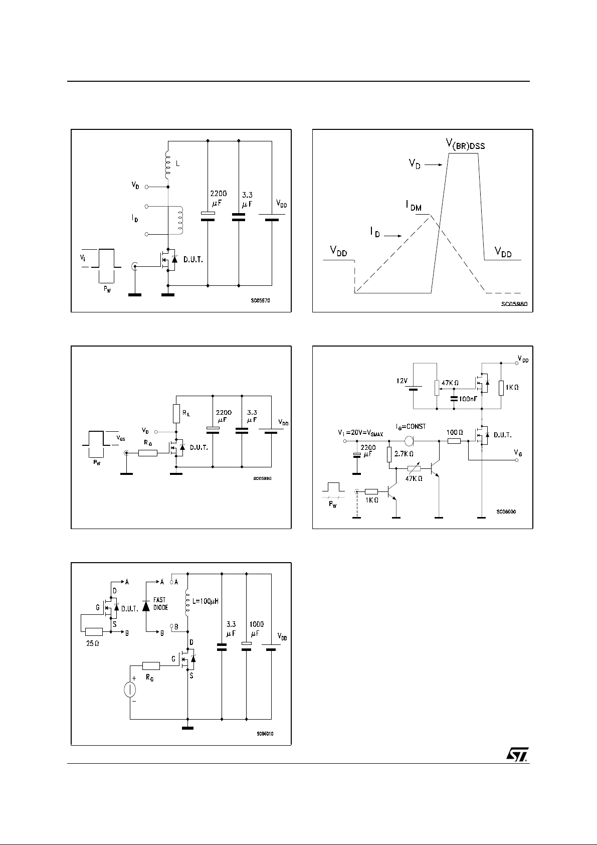
Figure 3: Unclamped Inductive Load Test Circuit
Figure 4: Switching Times Test Circuit For Resistive Load
Figure 6: Unclamped Inductive Wafeform
Figure 7: Gate Charge Test Circuit
Figure 5: Test Circuit For Inductive Load
Switching and Diode Recovery Times
4/12

STP25NM60N - STF25NM60N - STB25NM 60N/-1 - STW25NM60N
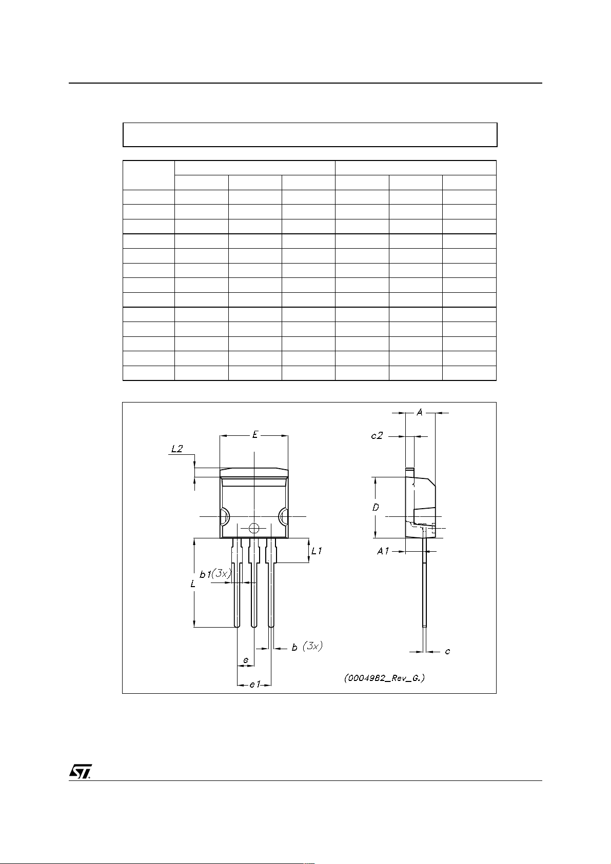
TO-220 MECHANICAL DATA
DIM.
A 4.40 4.60 0.173 0.181
b 0.61 0.88 0.024 0.034
b1 1.15 1.70 0.045 0.066
c 0.49 0.70 0.019 0.027
D 15.25 15.75 0.60 0.620
E 10 10.40 0.393 0.409
e 2.40 2.70 0.094 0.106
e1 4.95 5.15 0.194 0.202
F 1.23 1.32 0.048 0.052
H1 6.20 6.60 0.244 0.256
J1 2.40 2.72 0.094 0.107
L 13 14 0.511 0.551
L1 3.50 3.93 0.137 0.154
L20 16.40 0.645
L30 28.90 1.137
øP 3.75 3.85 0.147 0.151
Q 2.65 2.95 0.104 0.116
MIN. TYP MAX. MIN. TYP. MAX.
mm. inch
5/12

STP25NM60N - STF25NM60N - STB25NM 60N/-1 - STW25NM60N
TO-220FP MECHANICAL DATA
DIM.
A 4.4 4.6 0.173 0.181
B 2.5 2.7 0.098 0.106
D 2.5 2.75 0.098 0.108
E 0.45 0.7 0.017 0.027
F 0.75 1 0.030 0.039
F1 1.15 1.7 0.045 0.067
F2 1.15 1.7 0.045 0.067
G 4.95 5.2 0.195 0.204
G1 2.4 2.7 0.094 0.106
H 10 10.4 0.393 0.409
L2 16 0.630
L3 28.6 30.6 1.126 1.204
L4 9.8 10.6 .0385 0.417
L5 2.9 3.6 0.114 0.141
L6 15.9 16.4 0.626 0.645
L7 9 9.3 0.354 0.366
Ø 3 3.2 0.118 0.126
MIN. TYP MAX. MIN. TYP. MAX.
mm. inch
E
A
D
B
L3
L6
L7
F1
F
6/12
G1
H
F2
123
L4
L2
L5
G
STP25NM60N - STF25NM60N - STB25NM 60N/-1 - STW25NM60N
TO-262 (I2PAK) MECHANICAL DATA
DIM.
A 4.40 4.60 0.173 0.181
A1 2.40 2.72 0.094 0.107
b 0.61 0.88 0.024 0.034
b1 1.14 1.70 0.044 0.066
c 0.49 0.70 0.019 0.027
c2 1.23 1.32 0.048 0.052
D 8.95 9.35 0.352 0.368
e 2.40 2.70 0.094 0.106
e1 4.95 5.15 0.194 0.202
E 10 10.40 0.393 0.410
L 13 14 0.511 0.551
L1 3.50 3.93 0.137 0.154
L2 1.27 1.40 0.050 0.055
MIN. TYP MAX. MIN. TYP. MAX.
mm. inch
7/12

STP25NM60N - STF25NM60N - STB25NM 60N/-1 - STW25NM60N
TO-247 MECHANICAL DATA
DIM.
A 4.85 5.15 0.19 0.20
A1 2.20 2.60 0.086 0.102
b 1.0 1.40 0.039 0.055
b1 2.0 2.40 0.079 0.094
b2 3.0 3.40 0.118 0.134
c 0.40 0.80 0.015 0.03
D 19.85 20.15 0.781 0.793
E 15.45 15.75 0.608 0.620
e5.45 0.214
L 14.20 14.80 0.560 0.582
L1 3.70 4.30 0.14 0.17
L2 18.50 0.728
øP 3.55 3.65 0.140 0.143
øR 4.50 5.50 0.177 0.216
S5.50 0.216
MIN. TYP MAX. MIN. TYP. MAX.
mm. inch
8/12

STP25NM60N - STF25NM60N - STB25NM 60N/-1 - STW25NM60N
TO-252 (DPAK) MECHANICAL DATA
DIM.
A 2.20 2.40 0.087 0.094
A1 0.90 1.10 0.035 0.043
A2 0.03 0.23 0.001 0.009
B 0.64 0.90 0.025 0.035
B2 5.20 5.40 0.204 0.213
C 0.45 0.60 0.018 0.024
C2 0.48 0.60 0.019 0.024
D 6.00 6.20 0.236 0.244
E 6.40 6.60 0.252 0.260
G 4.40 4.60 0.173 0.181
H 9.35 10.10 0.368 0.398
L2 0.8 0.031
L4 0.60 1.00 0.024 0.039
V2 0
MIN. TYP. MAX. MIN. TYP. MAX.
o
mm inch
o
8
o
0
o
0
P032P_B
9/12

STP25NM60N - STF25NM60N - STB25NM 60N/-1 - STW25NM60N
D2PAK FOOTPRINT
TAPE AND REEL SHIPMENT
REEL MECHANICAL DATA
DIM.
MIN. MAX. MIN. MAX.
A 330 12.992
B 1.5 0.059
C 12.8 13.2 0.504 0.520
D 20.2 0795
G 24.4 26.4 0.960 1.039
N 100 3.937
T 30.4 1.197
mm inch
T APE MECHANICAL DATA
DIM.
A0 10.5 10.7 0.413 0.421
B0 15.7 15.9 0.618 0.626
D 1.5 1.6 0.059 0.063
D1 1.59 1.61 0.062 0.063
E 1.65 1.85 0.065 0.073
F 11.4 11.6 0.449 0.456
K0 4.8 5.0 0.189 0.197
P0 3.9 4.1 0.153 0.161
P1 11.9 12.1 0.468 0.476
P2 1.9 2.1 0.075 0.082
R 50 1.574
T 0.25 0.35 0.0098 0.0137
W 23.7 24.3 0.933 0.956
* on sales type
mm inch
MIN. MAX. MIN. MAX.
BASE QTY BULK QTY
1000 1000
10/12

STP25NM60N - STF25NM60N - STB25NM 60N/-1 - STW25NM60N
Table 9: Revision History
Date Revisio n Description of Change s
30-Nov-2004 1 First Release.
22-Mar-2005 2 Modified title
23-May-2005 3 Inserted some values in Tab7
08-Jun-2005 4 Inserted new row in table 6
11/12

STP25NM60N - STF25NM60N - STB25NM 60N/-1 - STW25NM60N
Information furnished is believed to be accurate and reliable. However, STMicroelectronics assumes no responsibility for the consequences
of use of such information nor for any infringement of patents or other rights of third parties which may result from its use. No license is granted
by implic ati o n or ot h er wis e und er an y pat ent or pa te nt r igh ts of STMi cr oe l ect ro ni cs . Sp ec if i cat i on s ment i o ned i n th is p ub li c ati on ar e s ubj ec t
to change without notice. This publication s upersedes and replaces all information previ ously supplied. STMicroelectronics products are not
authorized for use as critical components in life support devices or systems without express written approval of STMicroelectronics.
The ST logo is a registered trademark of STMicroelectronics
All other names are the property of their respective owners
© 2005 STMicroelectronics - All Rights Reserved
STMicroelectronics group of companies
Australia - Belgium - Brazil - Canada - China - Czech Republic - Finland - France - Germany - Hong Kong - India - Israel - Italy - Japan -
Malaysia - Malta - Morocco - Singapore - Spain - Sweden - Switzerland - United Kingdom - United States of America
12/12
 Loading...