

查询STB20NM60供应商
STP20NM60-STP20NM60FP-STW20NM60
STB20NM60 - STB20NM60-1
N-CHANNEL 600V - 0.25Ω - 20A TO-220/FP/D²/I²PAK/TO-247
MDmesh™ MOSFET
Table 1: Ge neral Features
TYPE V
STP20NM60
STP20NM60FP
STB20NM60
STB20NM60-1
STW20NM60
■ TYPICAL R
■ HIGH dv/dt AND AVALANCHE CAPABILITIES
■ 100% AVALANCHE TESTED
■ LOW INPUT CAPACITANCE AND GATE
DSS
600 V
600 V
600 V
600 V
600 V
(on) = 0.25 Ω
DS
R
DS(on)
< 0.29 Ω
< 0.29 Ω
< 0.29 Ω
< 0.29 Ω
< 0.29 Ω
I
D
20 A
20 A
20 A
20 A
20 A
CHARGE
■ LOW GATE INPUT RESISTAN CE
DESCRIPTION
The MDmesh™
is a new revolutionary MOSF ET
technology that asso ciates the Mul tiple Drain process with the Company’s PowerMESH™ horizontal layout. The resulting product has an
outstanding low on-resistance, impressively high
dv/dt and excellent avalanche characteristics. The
adoption of the Com pany’s proprietary strip technique yields overall dynamic p erformance that is
significantly better than that of similar competition’s products.
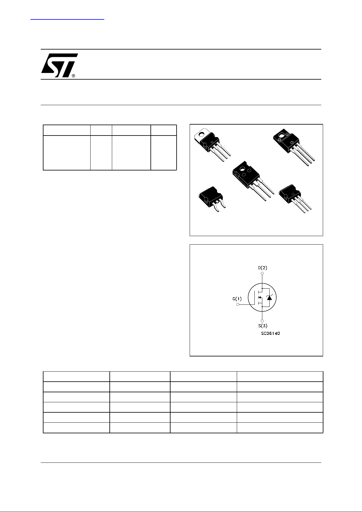
Figure 1: Package
3
2
1
TO-220
D²PAK
3
1
TO-247
1
3
2
TO-220FP
I²PAK
Figure 2: Internal Schematic Diagram
3
2
1
3
2
1
APPLICATIONS
The MDmesh™ family is very suitable for increasing power density of high voltage converters allowing system miniaturization and higher efficiencies.
Table 2: Order Codes
SALES TYPE MARKING PACKAGE PACKAGING
STP20NM60 P20NM60 TO-220 TUBE
STP20NM60FP P20NM60FP TO-220FP TUBE
STB20NM60T4 B20NM60 D²PAK TAPE & REEL
STB20NM60-1 B20NM60 I²PAK TUBE
STW20NM60 W20NM60 TO-247 TUBE
Rev.2
1/15February 2005
STP20NM60 - STP20NM60FP - STB20NM 60 - STW20NM60 - STB20NM60-1
Table 3: Absolute Maximum ratings
Symbol Parameter Value Unit
TO-220/D²PAK/
I²PAK/TO-247
V
I
V
V
DM
P
DGR
GS
I
I
TOT
DS
D
D
Drain-source Voltage (VGS = 0)
Drain-gate Voltage (RGS = 20 kΩ)
600 V
600 V
Gate- source Voltage ±30 V
Drain Current (continuous) at TC = 25°C
Drain Current (continuous) at TC = 100°C
()
Drain Current (pulsed) 80 80 (*) A
Total Dissipation at TC = 25°C
20 20 (*) A
12.6 12.6 (*) A
192 45 W
Derating Factor 1.2 0.36 W/°C
dv/dt (1) Peak Diode Recovery voltage slope 15 V/ns
V
ISO
T
stg
T
Insulation Winthstand Voltage (DC) -- 2500 V
Storage Temperature -65 to 150 °C
Max. Operating Junction Temperature 150 °C
j
() Pulse width limited by safe operating area
(1) I
≤ 20 A, di/dt ≤ 400 A/µs, V
SD
(*) Limited only by maximum temperature allowed
DD
≤ V
(BR)/DSS, Tj
≤ T
JMAX
TO-220FP
Table 4: Thermal Data
TO-220/D²PAK/
I²PAK/TO-247
Rthj-case Thermal Resistance Junction-case Max 0.65 2.8 °C/W
Rthj-amb Thermal Resistance Junction-ambient Max 62.5 °C/W
T
Maximum Lead Temperature For Soldering Purpose 300 °C
l
TO-220FP
Table 5: Avalanche Characteristics
Symbol Parame ter Max. Value Unit
I
AR
E
AS
Avalanche Current, Repetitive or Not-Repetitive
(pulse width limited by T
max)
j
Single Pulse Avalanche Energy
(starting T
= 25 °C, ID = IAR, VDD = 50 V)
j
ELECTRICAL CHARACTERISTICS (T
=25°C UNLESS OTHERWISE SPECIFIED)
CASE
10 A
650 mJ
Table 6: On/Off
Symbol Parameter Test Conditions Min. Typ. Max. Unit
V
(BR)DSS
I
DSS
I
GSS
V
GS(th)
R
DS(on)
Drain-source
Breakdown Voltage
Zero Gate Voltage
Drain Current (V
GS
= 0)
Gate-body Leakage
Current (V
DS
= 0)
Gate Threshold Voltage
Static Drain-source On
Resistance
ID = 250 µA, VGS = 0 600 V
= Max Rating
V
DS
VDS= Max Rating, TC= 125°C
V
= ± 30V ±100 µA
GS
V
= VGS, ID = 250 µA
DS
345V
1
10
VGS = 10V, ID = 10 A 0.25 0.29 Ω
Unit
µA
µA
2/15
STP20NM60 - STP20NM60FP - STB20NM60 - STW20NM60 - STB20NM60-1
ELECTRICAL CHARACTERISTICS (CONTINUED)
Table 7: Dynamic
Symbol Parameter Test Conditions Min. Typ. Max. Unit
(1) Forward Transconductance VDS > I
g
fs
C
oss eq.
C
iss
C
oss
C
rss
Input Capacitance
Output Capacitance
Reverse Transfer
Capacitance
(3) Equivalent Outpu t
Capacitance
t
d(on)
t
d(off)
Q
Q
Q
R
t
r
t
f
t
c
g
gs
gd
g
Turn-on Delay Time
Rise Time
Turn-off Delay Time
Fall Time
Cross-over Time
Total Gate Charge
Gate-Source Charge
Gate-Drain Charge
Gate Input Resistance f = 1 MHz Gate DC Bias = 0
ID = 10 A
V
DS
VGS = 0V, VDS = 0V to 400 V 215 pF
V
DD
RG = 4.7Ω VGS = 10 V
(Resistive Load see, Figure 3)
V
DD
(See test circuit, Figure 5)
V
DD
V
GS
Test Signal Level = 20 mV
Open Drain
D(on)
x R
DS(on)max,
11 S
= 25V, f = 1 MHz, VGS = 0 1500
350
35
= 200 V, ID = 10 A
25
20
6
= 480 V, ID = 20 A
11
21
= 400 V, ID = 20 A,
= 10V
39
10
20
1.6 Ω
54
pF
pF
pF
ns
ns
ns
ns
ns
nC
nC
nC
Table 8: Source Drain Diode
Symbol Parameter Test Conditions Min. Typ. Max. Unit
I
SD
I
SDM
VSD (1)
t
rr
Q
rr
I
RRM
t
rr
Q
rr
I
RRM
Note: 1. Pulsed: P ul se duration = 300 µs, duty cyc l e 1. 5 %.
2. Pulse wi dt h l i m ited by safe opera ting area.
3. C
Source-drain Current
(2)
Source-drain Current (pulsed)
Forward On Voltage
Reverse Recovery Time
Reverse Recovery Charge
Reverse Recovery Current
Reverse Recovery Time
Reverse Recovery Charge
Reverse Recovery Current
is defined as a constant equivalent capacitance giving the same charging time as C
oss eq.
V
.
DSS
ISD = 20 A, VGS = 0
I
SD
VDD = 100 V, Tj = 25°C
(see test circuit, Figure 5)
I
SD
V
DD
(see test circuit, Figure 5)
=20 A, di/dt = 100 A/µs
=20 A, di/dt = 100 A/µs
= 100 V, Tj = 150°C
390
5
25
510
6.5
26
when VDS increases from 0 to 80%
oss
20
80
1.5 V
A
A
ns
µC
A
ns
µC
A
3/15
STP20NM60 - STP20NM60FP - STB20NM 60 - STW20NM60 - STB20NM60-1
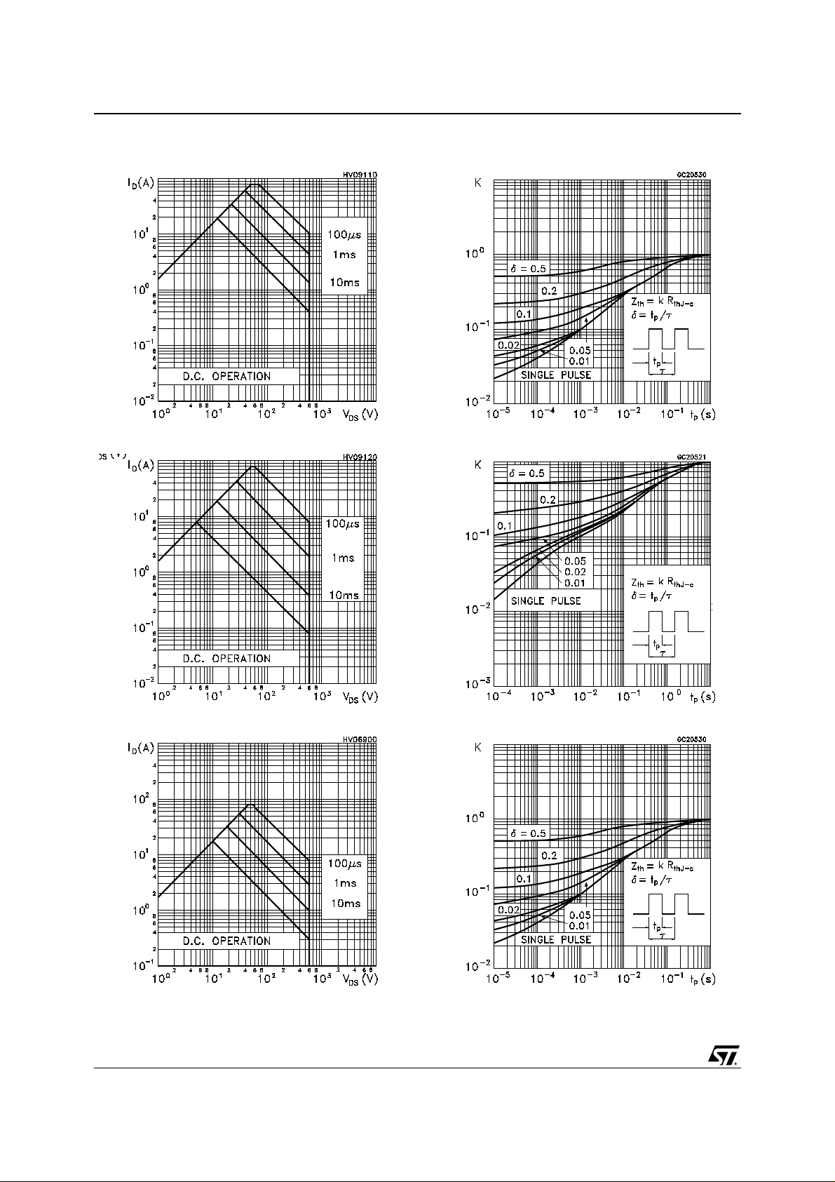
Figure 3: Safe Operating Area for TO-220/
D²PAK/I²PAK
Figure 4: Safe Operating Area for TO-220FP
Figure 6: Thermal Impedance for TO-220/
D²PAK/I²PAK
Figure 7: Thermal Impedan ce for TO -2 20FP
Figure 5: Safe Operating Area for TO-247
4/15
Figure 8: Thermal Impedan ce for TO -2 47
STP20NM60 - STP20NM60FP - STB20NM60 - STW20NM60 - STB20NM60-1
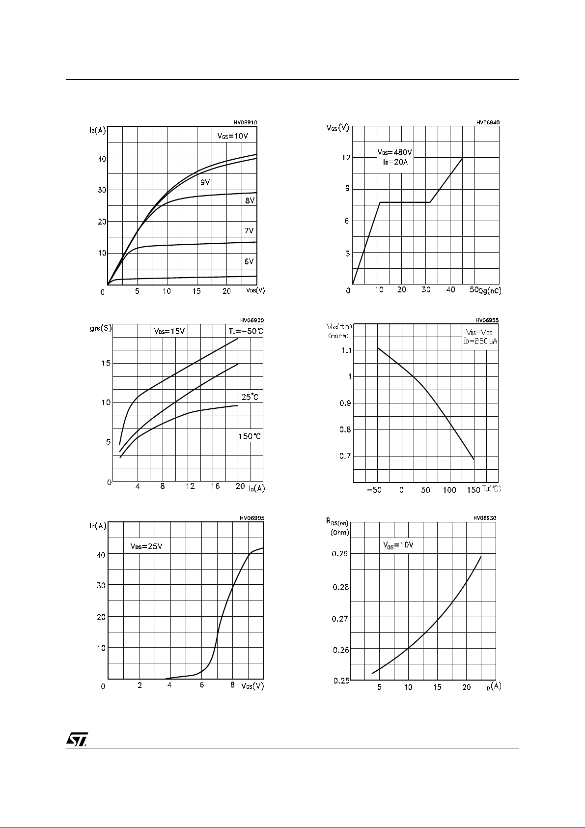
Figure 9: Output Characteristics
Figure 10: Transconductance
Figure 12: Gate Charge vs Gate-source Voltage
Figure 13: Normalized Gate Threshold Voltage
vs Tem p.
Figure 11: Transfer Characteristics
Figure 14: Static Drain-source On Resistance
5/15
 Loading...