

查询STB20NM50供应商
STB20NM50 - STB20NM50-1
STP20NM50 - STP20NM50FP
N-CHANNEL 550V@Tj
- 0.20Ω - 20A - TO220/FP-D²PAK-I²PAK
max
Zener-Protected SuperMESH™ MOSFET
General features
V
Type
STB20NM50
STB20NM50-1
STP20NM50
STP20NM50FP
■ HIGH dv/dt A ND AVALANCHE CAPABILITIES
■ 100% AVALANCHE TESTED
■ LOW INPUT CAPACITANCE AND GATE
DSS(@Tj
max)
550 V
550 V
550 V
550 V
CHARGE
■ LOW GATE INPUT RESISTANCE
Description
R
DS(on)
<0.25 Ω
<0.25 Ω
<0.25 Ω
<0.25 Ω
I
D
20 A
20 A
20 A
20 A
Package
3
2
TO-220
1
D²PAK
3
1
I²PAK
1
TO-220FP
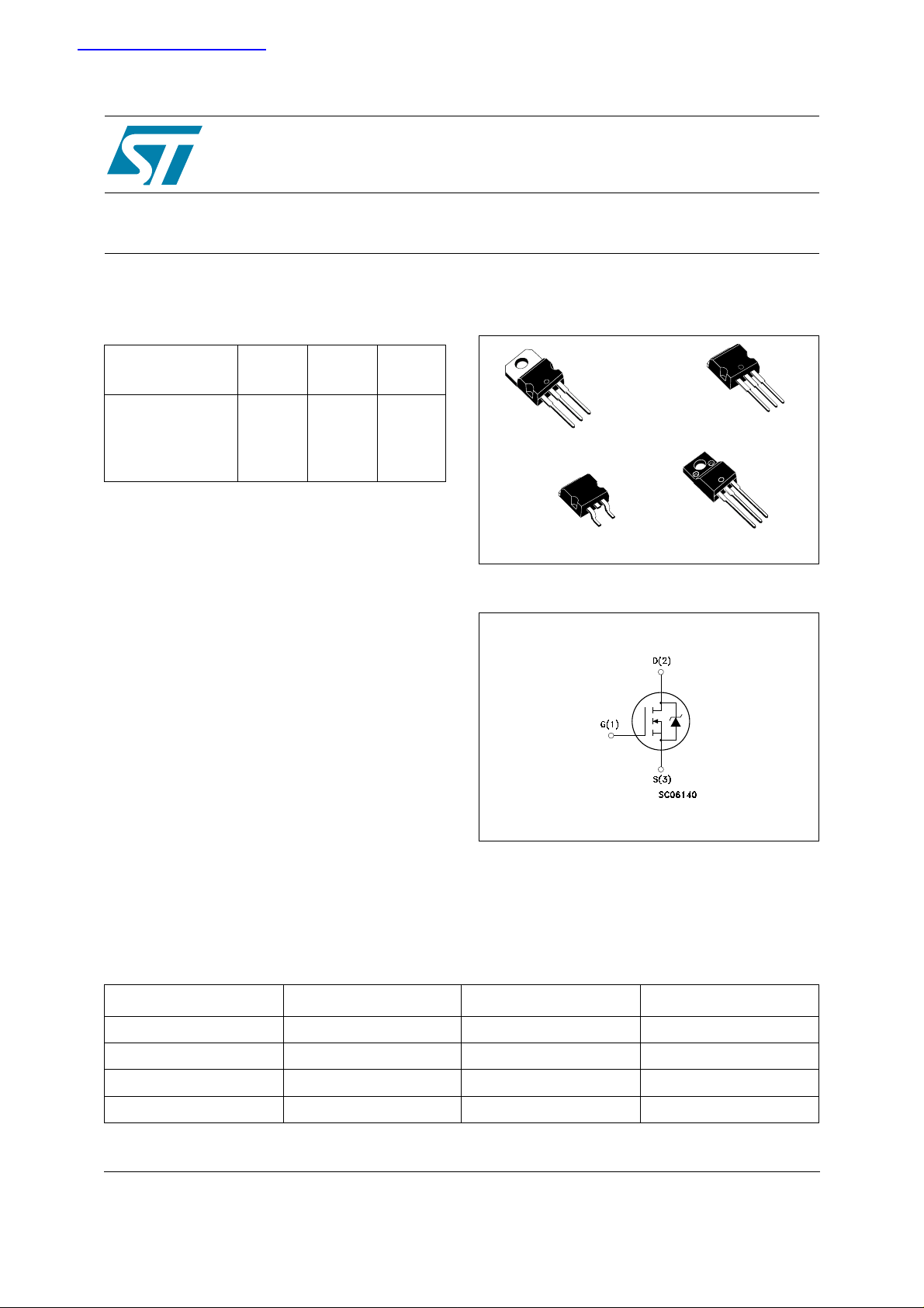
Internal schematic diagram
3
2
1
3
2
The MDmesh™ is a new revolutionary MOSFET
technology that associates the Multiple Drain
process with the Company’s
PowerMESH™horizontal layout. The resulting
product has an outstanding low on-resistance,
impressively high dv/dt and exellent avalanche
characteristics and dynamic performances.
Applications
The MDmesh™ family is very suitable for
increasing power density of high voltage
converters allowing system miniaturization
andhiher efficiencies
Order codes
Sales Type Marking Package Packaging
STB20NM50T4 B20NM50 D²PAK TAPE & REEL
STB20NM50-1 B20NM50-1 I²PAK TUBE
STP20NM505 P20NM50 TO-220 TUBE
STP20NM50FP P20NM50FP TO-220FP TUBE
Rev 2
September 2005 1/16
www.st.com
16
1 Electrical ratings STB20NM50-1 - STB20N M50 - STP2 0N M50 - STP20NM50F P
1 Electrical ratings
Table 1. Absolute maximum ratings
Symbol Parameter Value Unit
TO-220/D²PAK/I²PAK TO-220FP
I
DM
V
GS
I
D
I
D
Note 2
P
TOT
Gate-Source Voltage ± 30 V
Drain Current (continuous) at TC = 25°C
Drain Current (continuous) at TC = 100°C
20 20 (Note3) A
12.6 12.6 (Note 3) A
Drain Current (pulsed) 80 80 (Note3) A
Total Dissipation at TC = 25°C
192 45 W
Derating Factor 1.2 0.36 W/°C
dv/dt Note 1 Peak Diode Recovery voltage slope 15 V/ns
V
ISO
T
T
stg
Insulation Withstand Volatge (DC) -- 2000 V
Operating Junction Temperature
j
Storage Temperature
-65 to 150 °C
Table 2. Thermal data
TO-220/D²PAK/I²PAK TO-220FP Unit
Rthj-case Thermal Resistance Junction-case Max 0.65 2.8 °C/W
Rthj-amb Thermal Resist ance Junction-amb Max 62.5 °C/W
T
l
Maximum Lead Temperature For Solder ing
Purpose
300 °C
Table 3. Avalanche characteristics
Symbol Parameter Max Valu e Unit
I
AR
E
AS
2/16
Avalanche Curren t, repetitive or
Not-Repetitive (pul se width limited by Tj max)
Single Pulse Avalanche Energy
(starting Tj=25°C, I
=5A, VDD= 50V)
D
10 A
650 mJ
STB20NM 50-1 - STB20NM50 - ST P20NM50 - STP20NM 50FP 2 Electrical characteristics
2 Electrical characteristics
(T
= 25 °C unless otherwise specified)
CASE
Table 4. On/off states
Symbol Parameter Test Conditions Min. Typ. Max. Unit
V
(BR)DSS
I
DSS
I
GSS
V
GS(th)
R
DS(on)
Drain-Source Breakdown
Voltage
Zero Gate Voltage Drain
Current (V
GS
= 0)
Gate Body Leakage Current
= 0)
(V
DS
Gate Threshold Voltage
St ati c Drai n-Source On
Resistance
I
= 250µA, VGS= 0
D
= Max Ra ting,
V
DS
V
= Max Rating,Tc = 125°C
DS
= ±30V
V
GS
= VGS, ID = 250 µA
V
DS
V
= 10 V, ID= 10 A
GS
500 V
1
10
±100 µA
345V
0.20 0.25 Ω
Table 5. Dynamic
Symbol Parameter Test Conditions Min. Typ. Max. Unit
> I
V
DS
Note 4
g
fs
C
C
C
C
oss eq.
Note 5
iss
oss
rss
Forward Transconductance
Input Capaci tance
Outp u t C a pacita nce
Rev er se Trans fer Ca pa citan ce
Equivalent Ouput Capacitance
D(ON) xRDS(ON)max,
ID = 10A
=25V, f=1 MHz, VGS=0
V
DS
=0, V
V
GS
=0V to 400V
DS
10 S
1480
285
34
130 pF
µA
µA
pF
pF
pF
Rg Gate Input Resistance
Q
g
Q
gs
Q
gd
Total Gate Charge
Gate-Source Charge
Gate-Drain Charge
f=1MHz Gate DC Bias=0
Test Signal Level=20mV
Open Drain
=400V, ID = 20A
V
DD
=10V
V
GS
(see Figure 15)
1.6 Ω
40
13
19
56 nC
nC
nC
3/16

2 Electric al characteristics STB20N M 50-1 - STB20NM50 - ST P20NM 50 - STP20NM 50FP
Table 6. Switching times
Symbol Parameter Test Conditions Min. Typ. Max. Unit
V
=250 V, ID=10A,
t
d(on)
Tur n-o n Delay Time
t
r
Rise Time
DD
=4.7Ω, VGS=10V
R
G
(see Figure 16)
24
16
ns
ns
t
r(Voff)
t
Off-vol tage Rise Time
t
f
c
Fall Ti me
Cross-over T ime
=400 V, ID=20A,
V
DD
=4.7Ω, VGS=10V
R
G
(see Figure 16)
9
8.5
23
Table 7. Source drain diode
Symbol Parameter Test Conditions Min. Typ. Max. Unit
I
SD
I
Note 2
SDM
V
Note 4
SD
t
rr
Q
rr
I
RRM
t
rr
Q
rr
I
RRM
(1) ISD ≤20A, di/dt ≤400A/µs, VDD ≤ V
(2) Pul s e width limited by safe op erating area
(3) Limited only by maximum temperature allowed
(4) Pulsed: pulse duration = 300µs, duty cycle 1.5%
(5) C
oss eq.
to 80% V
Source-drain Current
Source-drain Current (pulsed)
, Tj ≤ T
JMAX
ISD=20A, VGS=0
=20A, di/dt = 100A/µs,
I
SD
V
=100 V, Tj=25°C
DD
=20A, di/dt = 100A/µs,
I
SD
V
=100 V, Tj=150°C
DD
Forward on Voltage
Reverse Recovery Time
Reverse Recovery Charge
Reverse Recovery Current
Reverse Recovery Time
Reverse Recovery Charge
Reverse Recovery Current
(BR)DSS
is defined as a constant equivalent capacitance giving the same charging time as C
DSS
20
80
1.5 V
350
4.6
26
435
5.9
27
when VDS increases from 0
oss
ns
ns
ns
A
A
ns
µC
A
ns
µC
A
4/16
STB20NM 50-1 - STB20NM50 - ST P20NM50 - STP20NM 50FP 2 Electrical characteristics
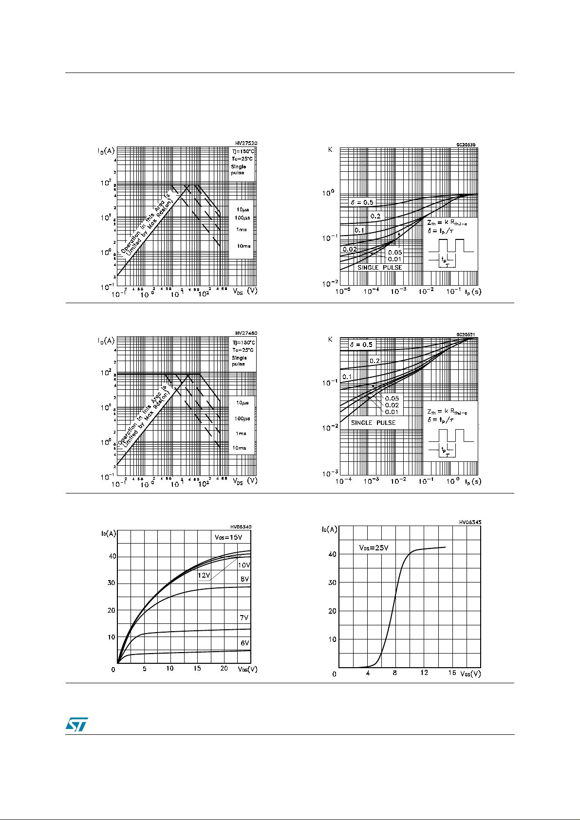
2.1 Electrical Characteristics (curves)
Figure 1. Safe Ope ra tin g A rea for
TO-220/D²PAK/I²PAK
Figure 3. Safe Operating Area for TO-220FP Figure 4. Th ermal Impedance for TO-220FP
Figure 2. Therm al Impedance for
TO-220/D²PAK/I²PAK
Figure 5. Output Characteristics Figure 6. Transfer Characteristics
5/16
 Loading...