

查询STB20NK50Z供应商
STP20NK50Z - STW20NK50Z
STB20NK50Z - STB20NK50Z-S
N-CHANNEL 500V -0.23Ω- 17A TO-220/D2PAK/I2SPAK/TO-247
Zener-Protected SuperMESH™ MOSFET
TYPE V
STB20NK50Z
STB20NK50Z-S
STP20NK50Z
STW20NK50Z
■ TYPICAL R
■ EXTREMELY HIGHdv/dt CAPABILITY
■ 100% AVALANCHE TESTEDGATE CHARGE
500 V
500 V
500 V
500 V
(on) = 0.23 Ω
DS
DSS
R
DS(on)
<0.27Ω
<0.27Ω
<0.27Ω
<0.27Ω
I
D
17 A
17 A
17 A
17 A
Pw
190 W
190 W
190 W
190 W
MINIMIZED
■ VERY LOW INTRINSIC CAPACITANCES
■ VERY GOOD MANUFACTURING
REPEATIBILITY
DESCRIPTION
The SuperMESH™ series is obtained through an
extreme optimization of ST’s well established stripbased PowerMESH™ layout. In addition to pushing
on-resistance significantly down,specialcareis taken to ensure a very good dv/dt capability for the
most dem anding applications. Such series complements ST ful l range of high voltage MOSFETs including revolutionary MDm es h™ products.
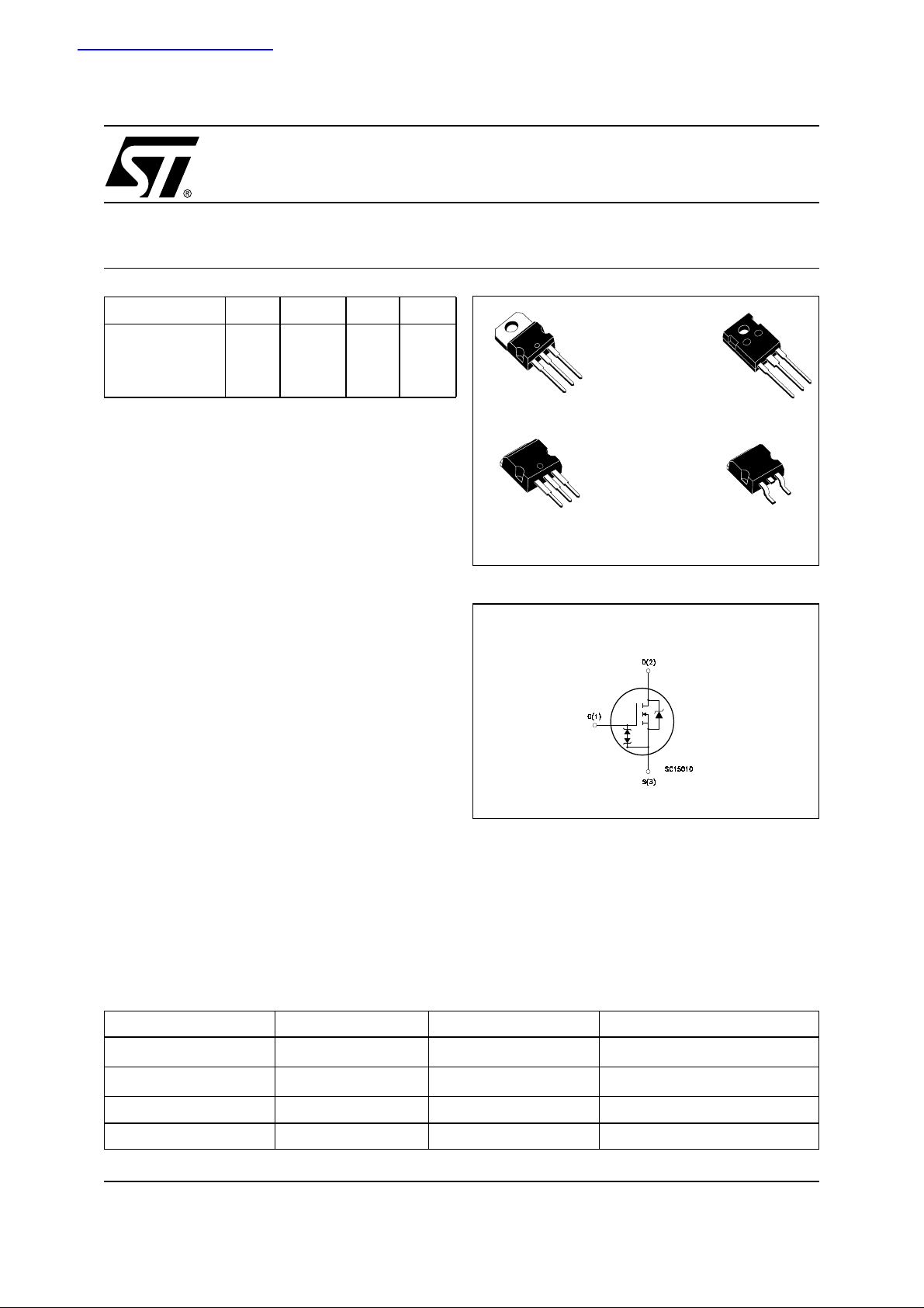
3
2
1
TO-220
I2SPAK
3
2
1
TO-247
D2PAK
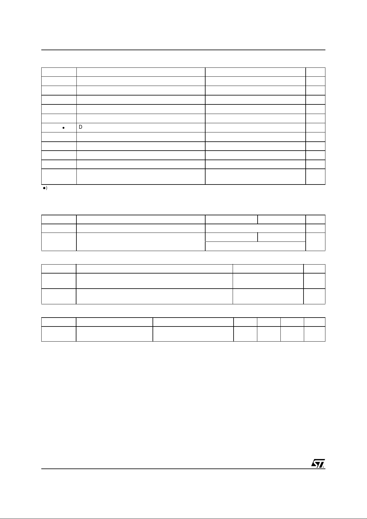
INTERNAL SCHEMATIC DIAGRAM
3
2
1
3
1
APPLICATIONS
■ HIGH CURRENT, HIGH SPEED SWITCHING
■ IDEAL FOR OFF-LINE POWER SUPPLIES,
ADAPTORS AND PFC
ORDERING INFORMATION
SALES TYPE MARKING PACKAGE PACKAGING
STB20NK50ZT4 B20NK50Z
STB20NK50Z-S B20NK50Z
STP20NK50Z P20NK50Z TO-220 TUBE
STW20NK50Z W20NK50Z TO-247 TUBE
2
D
2
I
SPAK
PAK
TAPE & REEL
TUBE
1/13May 2004
STP20NK50Z - STB20NK50Z - ST W20N K 50Z - STB20NK50Z-S
ABSOLUTE MAXIMUM RATINGS
Symbol Parameter Value Unit
V
DS
V
DGR
V
GS
I
D
I
D
IDM()
P
TOT
V
ESD(G-S)
dv/dt (1) Peak Diode Recovery voltage slope 4.5 V/ns
T
j
T
stg
() Pulse width limited by safe operating area
≤17A, di/dt ≤200A/µs, VDD≤ V
(1) I
SD
(*) Limited only by m aximum temperature allowed
THERMAL DATA
Rthj-case Thermal Resistance Junction-case Max 0.66 °C/W
Rthj-amb Thermal Resistance Junction-ambient Max 62.5 50 °C/W
T
l
Drain-source Voltage (VGS=0)
Drain-gate Voltage (RGS=20kΩ)
500 V
500 V
Gate- source Voltage ± 30 V
Drain Current (continuous) at TC=25°C
Drain Current (continuous) at TC= 100°C
17 A
10.71 A
Drain Current (pulsed) 68 A
Total Dissipation at TC=25°C
190 W
Derating Factor 1.51 W/°C
Gate source ESD(HBM-C=100 pF, R=1.5 KΩ) 6000 V
Operating Junction Temperature
Storage Temperature
(BR)DSS,Tj
≤ T
JMAX.
-55 to 150 °C
TO-220/D2PAK TO-247
Maximum Lead Temperature For Soldering Purpose 300
°C
AVALANCHE CHARACTERISTICS
Symbol Parameter Max Value Unit
I
AR
E
AS
Avalanche Current, Repetitive or Not-Repetitive
(pulse width limited by T
max)
j
Single Pulse Avalanche Energy
(starting T
=25°C, ID=IAR,VDD=50V)
j
17 A
850 mJ
GATE-SOURCE ZENER DIODE
Symbol Parameter Test Conditions Min. Typ. Max. Unit
BV
GSO
Gate-Source Breakdown
Igs=± 1mA (Open Drain) 30 V
Voltage
PROTECTION FEATURES OF GATE-TO-SOURCE ZENER DIODES
The built-in back-to-back Zener diodes have specifically been designed to enhance not only the device’s
ESD capability, but also to make t hem s afely absorb pos sible voltage transients that may occasionally be
applied from gate to source. In this respect the Zener voltage is appropriate to achieve an efficient and
cost-effective intervention to prote ct the device’s integrity. These integrated Zener diodes thus avoid the
usage of external components.
2/13
STP20NK50Z - STB20NK50Z - STW20NK50Z - STB20NK50Z-S
ELECTRICAL CHARACTERISTICS (T
=25°C UNLESS O THERWISE SPECIFIED)
CASE
ON/OFF
Symbol Parameter Test Conditions Min. Typ. Max. Unit
V
(BR)DSS
Drain-source
ID=1mA,VGS= 0 500 V
Breakdown Voltage
I
DSS
I
GSS
V
GS(th)
R
DS(on)
Zero Gate Voltage
Drain Current (V
GS
=0)
Gate-body Leakage
Current (V
DS
=0)
Gate Threshold Voltage
Static Drain-source On
V
=MaxRating
DS
=MaxRating,TC= 125 °C
V
DS
V
= ± 20 V ±10 µA
GS
V
DS=VGS,ID
= 100 µA
3 3.75 4.5 V
1
50
VGS=10V,ID= 8.5 A 0.23 0.27 Ω
Resistance
DYNAMIC
Symbol Parameter Test Conditions Min. Typ. Max. Unit
g
(1) Forward Transconductance VDS=15V,ID=8.5A 13 S
fs
C
oss eq.
C
iss
C
oss
C
rss
Input Capacitance
Output Capacitance
Reverse Transfer
Capacitance
(3) Equivalent Output
=25V,f=1MHz,VGS= 0 2600
V
DS
328
72
VGS=0V,VDS= 0V to 640V 187 pF
Capacitance
SWITCHING ON/OFF
Symbol Parameter Test Conditions Min. Typ. Max. Unit
t
d(on)
t
d(off)
Q
Q
Q
t
r
t
f
g
gs
gd
Turn-on Delay Time
Rise Time
Turn-off Delay Time
Fall Time
Total Gate Charge
Gate-Source Charge
Gate-Drain Charge
=250V,ID=8.5A
V
DD
RG=4.7Ω , VGS=10V
(Resistive Load see, Figure 3)
=400V,ID=17A,
V
DD
V
=10V
GS
28
20
70
15
85
15.5
42
119
µA
µA
pF
pF
pF
ns
ns
ns
ns
nC
nC
nC
SOURCE DRAIN DIODE
Symbol Parameter Test Conditions Min. Typ. Max. Unit
I
SD
I
SDM
V
SD
t
rr
Q
rr
I
RRM
t
rr
Q
rr
I
RRM
Note: 1. Pulsed: Pulse duration = 300 µs, duty cycle 1.5 %.
2. Pulse width limited by safe operating area.
3. C
Source-drain Current
(2)
Source-drain Current (pulsed)
(1)
ForwardOnVoltage
Reverse Recovery Time
Reverse Recovery Charge
Reverse Recovery Current
Reverse Recovery Time
Reverse Recovery Charge
Reverse Recovery Current
is defined as a constant equivalent capacitance giving the same charging time as C
oss eq.
.
V
DSS
ISD=17A,VGS=0
I
SD
V
R
(see test circuit, Figure 5)
I
SD
V
R
(see test circuit, Figure 5)
=17A,di/dt=100A/µs
= 100 V, Tj=25°C
=17A,di/dt=100A/µs
= 100 V, Tj=150°C
355
3.90
22
440
5.72
26
when VDSincreases from 0 to 80%
oss
17
68
1.6 V
A
A
ns
µC
A
ns
µC
A
3/13
STP20NK50Z - STB20NK50Z - ST W20N K 50Z - STB20NK50Z-S
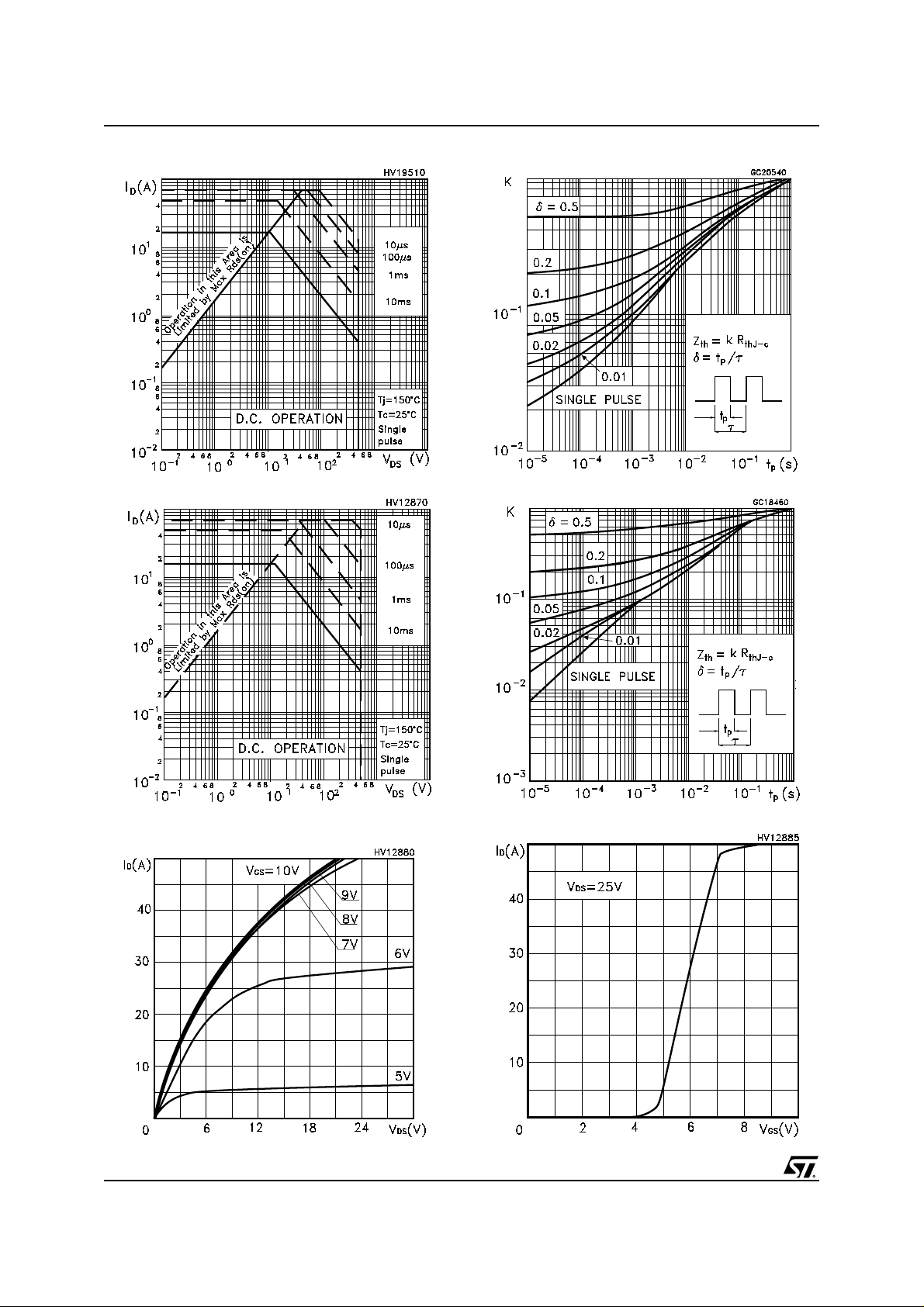
Safe Operating A rea for TO-220 / D2PAK/ I2SPAK Thermal Impedance fo r TO -220 / D2PAK/I2SPAK
Thermal Impedance for TO-247Safe Operating Area for TO-247
Output Characteristics
4/13
Transfer Characteristics
STP20NK50Z - STB20NK50Z - STW20NK50Z - STB20NK50Z-S
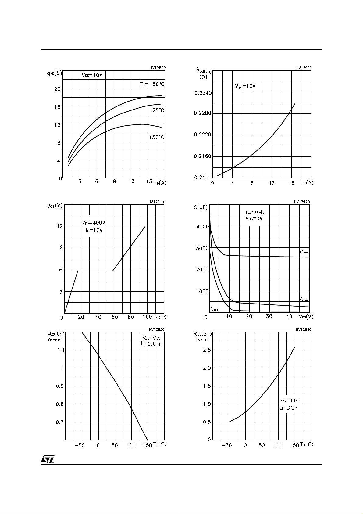
Static Drain-source On ResistanceTransconductance
Gate Charge vs Gate-so urc e V oltage Capacitance Variations
Normalized On Resistance vs TemperatureNormalized Gate Threshold Voltage vs Temp.
5/13

STP20NK50Z - STB20NK50Z - ST W20N K 50Z - STB20NK50Z-S
Source-drain Diode Forward Characteristics
Maximum Avalanche Energy vs Temperature
Normalized BVDSS vs Temperature
6/13

STP20NK50Z - STB20NK50Z - STW20NK50Z - STB20NK50Z-S
Fig. 2: Unclamped Inductive WaveformFig. 1: Unclamped Inductive Load Test Circuit
Fig. 3: Switching Times Test Circuit For
Resistive Load
Fig. 5: Test Circuit For Inductive Load Switching
And Di ode Recovery Times
Fig. 4: Gate Charge test Circuit
7/13

STP20NK50Z - STB20NK50Z - ST W20N K 50Z - STB20NK50Z-S
TO-220 MECHANICAL DATA
DIM.
A 4.40 4.60 0.173 0.181
b 0.61 0.88 0.024 0.034
b1 1.15 1.70 0.045 0.066
c 0.49 0.70 0.019 0.027
D 15.25 15.75 0.60 0.620
E 10 10.40 0.393 0.409
e 2.40 2.70 0.094 0.106
e1 4.95 5.15 0.194 0.202
F 1.23 1.32 0.048 0.052
H1 6.20 6.60 0.244 0.256
J1 2.40 2.72 0.094 0.107
L 13 14 0.511 0.551
L1 3.50 3.93 0.137 0.154
L20 16.40 0.645
L30 28.90 1.137
øP 3.75 3.85 0.147 0.151
Q 2.65 2.95 0.104 0.116
MIN. TYP MAX. MIN. TYP. MAX.
mm. inch
8/13

STP20NK50Z - STB20NK50Z - STW20NK50Z - STB20NK50Z-S
D2PAK MECHANICAL DATA
DIM.
MIN. TYP MAX. MIN. TYP. MAX.
A 4.4 4.6 0.173 0.181
A1 2.49 2.69 0.098 0.106
A2 0.03 0.23 0.001 0.009
B 0.7 0.93 0.027 0.036
B2 1.14 1.7 0.044 0.067
C 0.45 0.6 0.017 0.023
C2 1.23 1.36 0.048 0.053
D 8.95 9.35 0.352 0.368
D1 8 0.315
E 10 10.4 0.393
E1 8.5 0.334
G 4.88 5.28 0.192 0.208
L 15 15.85 0.590 0.625
L2 1.27 1.4 0.050 0.055
L3 1.4 1.75 0.055 0.068
mm. inch
M 2.4 3.2 0.094 0.126
3
1
9/13

STP20NK50Z - STB20NK50Z - ST W20N K 50Z - STB20NK50Z-S
TO-247 MECHANICAL DATA
DIM.
A 4.85 5.15 0.19 0.20
D 2.20 2.60 0.08 0.10
E 0.40 0.80 0.015 0.03
F 1 1.40 0.04 0.05
F1 3 0.11
F2 2 0.07
F3 2 2.40 0.07 0.09
F4 3 3.40 0.11 0.13
G 10.90 0.43
H 15.45 15.75 0.60 0.62
L 19.85 20.15 0.78 0.79
L1 3.70 4.30 0.14 0.17
L2 18.50 0.72
L3 14.20 14.80 0.56 0.58
L4 34.60 1.36
L5 5.50 0.21
M 2 3 0.07 0.11
V
V2
Dia 3.55 3.65 0.14 0.143
MIN. TYP MAX. MIN. TYP. MAX.
mm. inch
5º 5º
60º 60º
10/13

STP20NK50Z - STB20NK50Z - STW20NK50Z - STB20NK50Z-S
I2SPAK MECHANICAL DATA
DIM.
A 4.40 4.60 0.173 0.181
A1 2.49 2.69 0.098 0.106
B 0.70 0.93 0.027 0.037
B2 1.14 1.70 0.045 0.067
C 0.45 0.60 0.018 0.024
C2 1.23 1.36 0.048 0.053
D 8.95 9.35 0.352 0.368
E 10.00 10.40 0.394 0.409
G 4.88 5.28 0.192 0.208
L 16.7 17.5 0.657 0.689
L2 1.27 1.4 0.05 0.055
L3 13.82 14.42 0.544 0.568
MIN. TYP MAX. MIN. TYP. MAX.
mm. inch
11/13
STP20NK50Z - STB20NK50Z - ST W20N K 50Z - STB20NK50Z-S
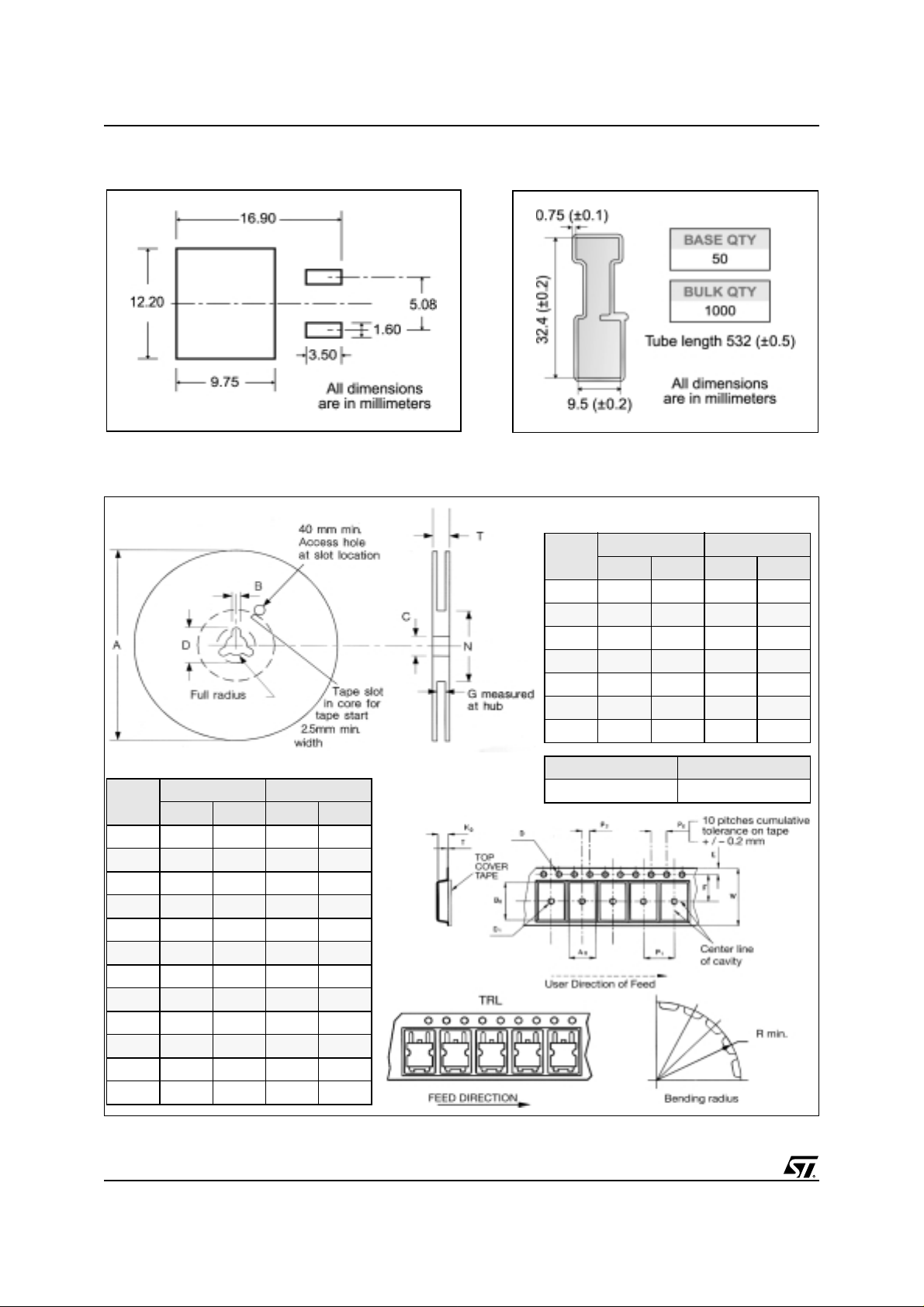
D2PAK FOOTPRINT
TAPE AND REEL SHIPMENT (suffix ”T4”)*
TUBE SHIPMENT (no suffix)*
REEL MECHANICAL DATA
DIM.
A 330 12.992
B 1.5 0.059
C 12.8 13.2 0.504 0.520
D 20.2 0795
G 24. 4 26.4 0.960 1.039
N 100 3.937
T 30.4 1.197
mm inch
MIN. MAX. MIN. MAX.
TAPE MECHANICAL DATA
DIM.
A0 10.5 10.7 0.413 0.421
B0 15.7 15.9 0.618 0 .626
D 1.5 1.6 0.059 0.063
D1 1.59 1.61 0.062 0.063
E 1.65 1.85 0.065 0.073
F 11.4 11.6 0.449 0.456
K0 4.8 5. 0 0.189 0.197
P0 3.9 4.1 0.153 0.161
P1 11.9 12.1 0.468 0.476
P2 1.9 2.1 0.075 0.082
R 50 1.574
T 0.25 0.35 0.0098 0.0137
* on sales ty pe
12/13
mm inch
MIN. MAX. MIN. MAX.
BASE QTY BULK QTY
1000 1000

STP20NK50Z - STB20NK50Z - STW20NK50Z - STB20NK50Z-S
Information furnished is believed to be accurate and reliable. However, STMicroelectronics assumes no responsibility for the
consequences of u se of suc h informat ion n or for any in fring ement of paten ts or oth er ri ghts of th ird part ies whic h may resul t from
its use. No license is granted by implication or otherwise under any patent or patent rights of STMicroelectronics. Specifications
mentioned in this publication are subject to change without notice. This publication supersedes and replaces all information
previously supplied. STMicroelectronics products are not authorized for use as critical components in life support devices or
systems without express written approval of STMicroelectronics.
Australia - Belgium - Brazil - Canada - China - Czech Republic - Finland - France - Germany - Hong Kong - India - Israel - Italy - Japan -
Malaysia - Malta - Morocco - Singapore - Spain - Sweden - Switzerland - United Kingdom - United States.
The ST logo is a registered trademark of STMicroelectronics
All other names are the property of their respective owners
© 2004 STMicroelectronics - All Rights Reserved
STMicroelectronics GROUP OF COMPANIES
http://www.st.com
13/13
 Loading...