

ST STP14NK60Z, STP14NK60ZFP, STB14NK60Z, STB14NK60Z-1, STW14NK60Z User Manual
1
3
1
3
3
3
1
3
查询STB14NK60供应商
STP14NK60Z - STP14NK60ZFP
STB14NK60Z/-1 - STW14NK60Z
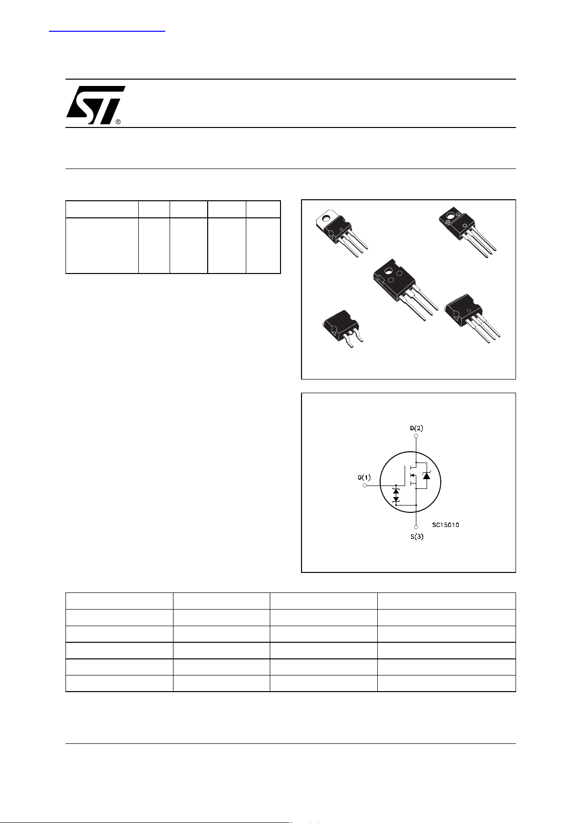
N-CHANNEL 600V - 0.45Ω - 13.5A TO-220/FP-D²/I²PAK-TO-247
Zener-Protected SuperMESH™ MOSFET
Table 1: General Features
TYPE V
STP14NK60Z
STP14NK60ZFP
STB14NK60Z
STB14NK60Z-1
STW14NK60Z
■ TYPICAL R
■ EXTREMELY HIGH dv /d t CAPABILITY
■ 100% AVALANCHE TESTED
■ GATE CHARGE MINIMIZED
■ VERY LOW INTRINSIC CAPACITANCES
■ VERY GOOD MANUFACTURING
DSSRDS(on)
600 V
600 V
600 V
600 V
600 V
(on) = 0.45 Ω
DS
< 0.5 Ω
< 0.5 Ω
< 0.5 Ω
< 0.5 Ω
< 0.5 Ω
I
D
13.5 A
13.5 A
13.5 A
13.5 A
13.5 A
Pw
160 W
40 W
160 W
160 W
160 W
REPEATIBILITY
DESCRIPTION
The SuperMESH™ series is obtained through an
extreme optimization of ST’s well established
strip-based PowerMESH™ layout. In addition to
pushing on-resistance significantly down, special
care is taken to ensure a very good dv/dt capability
for the most demanding applications. Such series
complements ST full range of high voltage MOS
-
FET s including revolutionary MDmesh™ products.
Figure 1: Package
2
TO-220
TO-220P
2
TO-247
1
D²PAK
I²PAK
Figure 2: Internal Schematic Diagram
2
2
1
APPLICATIONS
■ HIGH CURRENT, HIGH SPEED SWITCHING
■ IDEAL F OR OFF-LINE POWER SUP PLIE S,
ADAPTORS AND PFC
■ LIGHTING
Table 2: Order Codes
Part Number Marking Package Packaging
STP14NK60Z P14NK60Z TO-220 TUBE
STP14NK60ZFP P14NK60ZFP TO-220FP TUBE
STB14NK60ZT4 B14NK60Z D²PAK TAPE & REEL
STB14NK60Z-1 B14NK60Z I²PAK TUBE
STW14NK60Z W14NK60Z TO-247 TUBE
Rev. 4
1/17September 2005
STP14NK60Z - STP14NK60ZFP - STB14NK60Z - STB14NK60Z-1 - STW14NK60Z
Table 3: Absolute Maximum ratings
Symbol Parameter Value Unit
TO-220/D²PAK/I²PAK
TO-247
V
I
V
V
DM
P
DGR
I
I
TOT
Drain-source Voltage (VGS = 0)
DS
Drain-gate Voltage (RGS = 20 kΩ)
Gate-source Voltage ± 30 V
GS
Drain Current (continuous) at TC = 25°C
D
Drain Current (continuous) at TC = 100°C
D
()
Drain Current (pulsed) 54 54 (*) A
Total Dissipation at TC = 25°C
13.5 13.5 (*) A
8.5 8.5 (*) A
160 40 W
600 V
600 V
Derating Factor 1.28 0.32 W/°C
V
ESD(G-S)
Gate source ESD (HBM-C= 100pF, R= 1.5kΩ) 4000 V
dv/dt (1) Peak Diode Recovery voltage slope 4.5 V/ns
V
T
T
Insulation Winthstand Voltage (DC) -- 2500 V
ISO
Operating Junction Temperature
j
Storage Temperature
stg
-55 to 150 °C
() Pulse width limited by safe operating area
(1) ISD ≤ 13.5A, di/dt ≤ 200 A/µs, VDD ≤ V
(*) Limited only by maximum temperature allowed
(BR)DSS
, Tj ≤ T
JMAX.
TO-220FP
Table 4: Thermal Data
TO-220/D²PAK/I²PAK
TO-247
Rthj-case Thermal Resistance Junction-case Max 0.78 3.1 °C/W
Rthj-amb Thermal Resistance Junction-ambient Max 62.5 50 °C/W
T
Maximum Lead Temperature For Soldering Purpose
l
300 °C
TO-220FP Unit
Table 5: Avalanche Characteristics
Symbol Parameter Max Value Unit
I
AR
Avalanche Current, Repetitive or Not-Repetitive
12 A
(pulse width limited by Tj max)
E
Single Pulse Avalanche Energy
AS
300 mJ
(starting Tj = 25 °C, ID = IAR, VDD = 50 V)
Table 6: Gate-Source Zener D io de
Symbol Parameter Test Conditions Min. Typ. Max. Unit
BV
Gate source Breakdown
GSO
Igs= ± 1 mA (Open Drain) 30 V
Voltage
PROTECTION FEATURES OF GATE-TO-SOURCE ZENER DIODES
The built-in back-to-back Zener diodes have sp ecifically been desig ned to enhance not only the dev ice’s
ESD capability, but also to make them safely absorb possible voltage transients that may occasionally be
applied from gate to source. In this respect the Zener voltage is appropriate to achieve an ef ficient and
cost-effective intervention t o protec t t he d ev ice’s i ntegrity. T hese integrated Zener diodes thus avoid the
usage of external components.
2/17
STP14NK60Z - STP14NK60ZFP - STB14NK60Z - STB14NK60Z-1 - ST W14N K60Z
ELECTRICAL CHARACTERISTICS (T
=25°C UNLESS OTHERWISE SPECIFIED)
CASE
Table 7: On/Off
Symbol Parameter Test Conditions Min. Typ. Max. Unit
V
(BR)DSS
Drain-source
ID = 1mA, VGS = 0 600 V
Breakdown Voltage
I
DSS
I
GSS
Zero Gate Voltage
Drain Current (VGS = 0)
Gate-body Leakage
VDS = Max Rating
VDS = Max Rating, TC = 125 °C
1
50
VGS = ± 30V ±10 µA
Current (VDS = 0)
V
GS(th)
R
DS(on)
Gate Threshold Voltage
Static Drain-source On
VDS = VGS, ID = 100 µA
3 3.75 4.5 V
VGS = 10V, ID = 6 A 0.45 0.5 Ω
Resistance
Table 8: Dynamic
Symbol Parameter Test Conditions Min. Typ. Max. Unit
g
C
oss eq.
fs
C
C
C
t
d(on)
t
d(off)
Q
Q
Q
(1)
iss
oss
rss
t
r
t
f
gs
gd
Forward Transconductance
Input Capacitance
Output Capacitance
Reverse Transfer Capacitance
(3)
Equivalent Output Capacitance
Turn-on Delay Time
Rise Time
Turn-off Delay Time
Fall Time
Total Gate Charge
g
Gate-Source Charge
Gate-Drain Charge
VDS = 15 V, ID= 6 A 11 S
VDS = 25V, f = 1 MHz, VGS = 0 2220
240
57
VGS = 0V, VDS = 0V to 480V 122
VDD = 300 V, ID = 6 A,
RG= 4.7 Ω, VGS = 10 V
(Resistive Load see, Figure 21)
26
18
62
13
VDD = 480V, ID = 12 A,
VGS = 10V
(see, Figure 24)
75
13.2
38.6
µA
µA
pF
pF
pF
pF
ns
ns
ns
ns
nC
nC
nC
Table 9: Source Drain Diode
Symbol Parameter Test Conditions Min. Typ. Max. Unit
I
SD
I
SDM
VSD (1)
t
rr
Q
I
RRM
t
rr
Q
I
RRM
(1) Pulsed: Pulse du rat i on = 300 µs, du ty cycle 1.5 % .
(2) Pulse width limited by safe operating area.
(3) C
oss eq.
Source-drain Current
Source-drain Current (pulsed)
(2)
Forward On Voltage
Reverse Recovery Time
Reverse Recovery Charge
rr
Reverse Recovery Current
Reverse Recovery Time
Reverse Recovery Charge
rr
Reverse Recovery Current
is defined as a constant equivalent capacitance giving the same charging time as Coss when VDS increases from 0 to 80% VDSS
ISD = 12 A, VGS = 0
ISD = 12 A, di/dt = 100 A/µs
VDD = 50 V, Tj = 25°C
(see test circuit, Figure 22)
ISD = 12 A, di/dt = 100 A/µs
VDD = 50 V, Tj = 150°C
(see test circuit, Figure 22)
490
4.7
19.3
664
6.8
20.5
12
48
1.6 V
A
A
ns
µC
A
ns
µC
A
3/17
STP14NK60Z - STP14NK60ZFP - STB14NK60Z - STB14NK60Z-1 - STW14NK60Z
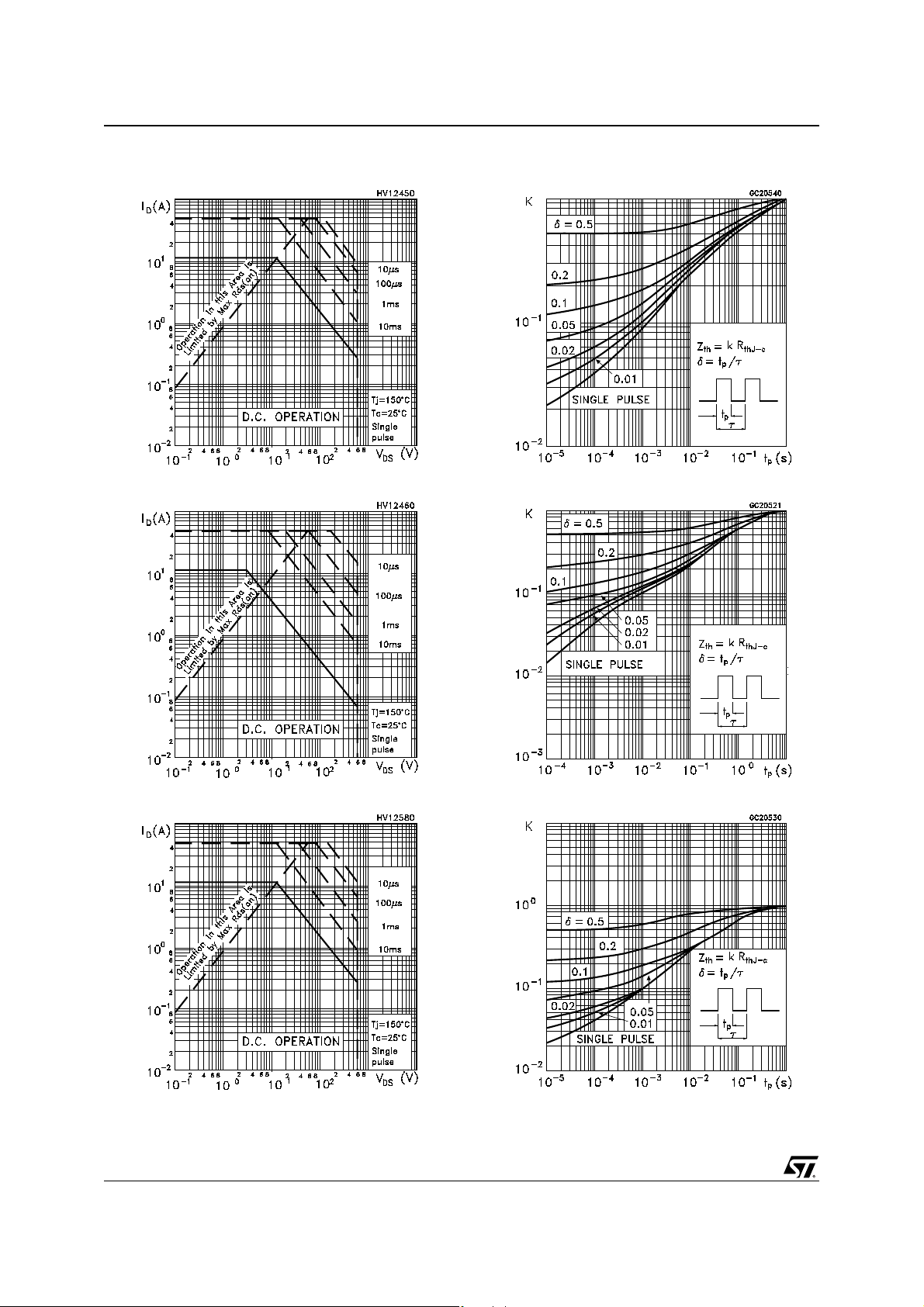
Figure 3: .Safe Operating Area For TO-220/
D²PAK/I²PAK
Figure 4: Safe Operating Area For TO-220FP
Figure 6: Thermal Impedance For TO-220/
D²PAK/I²PAK
Figure 7: Thermal Impedance For TO-220FP
Figure 5: Safe Operating Area For TO-247
4/17
Figure 8: Thermal Impedance For TO-247
STP14NK60Z - STP14NK60ZFP - STB14NK60Z - STB14NK60Z-1 - ST W14N K60Z
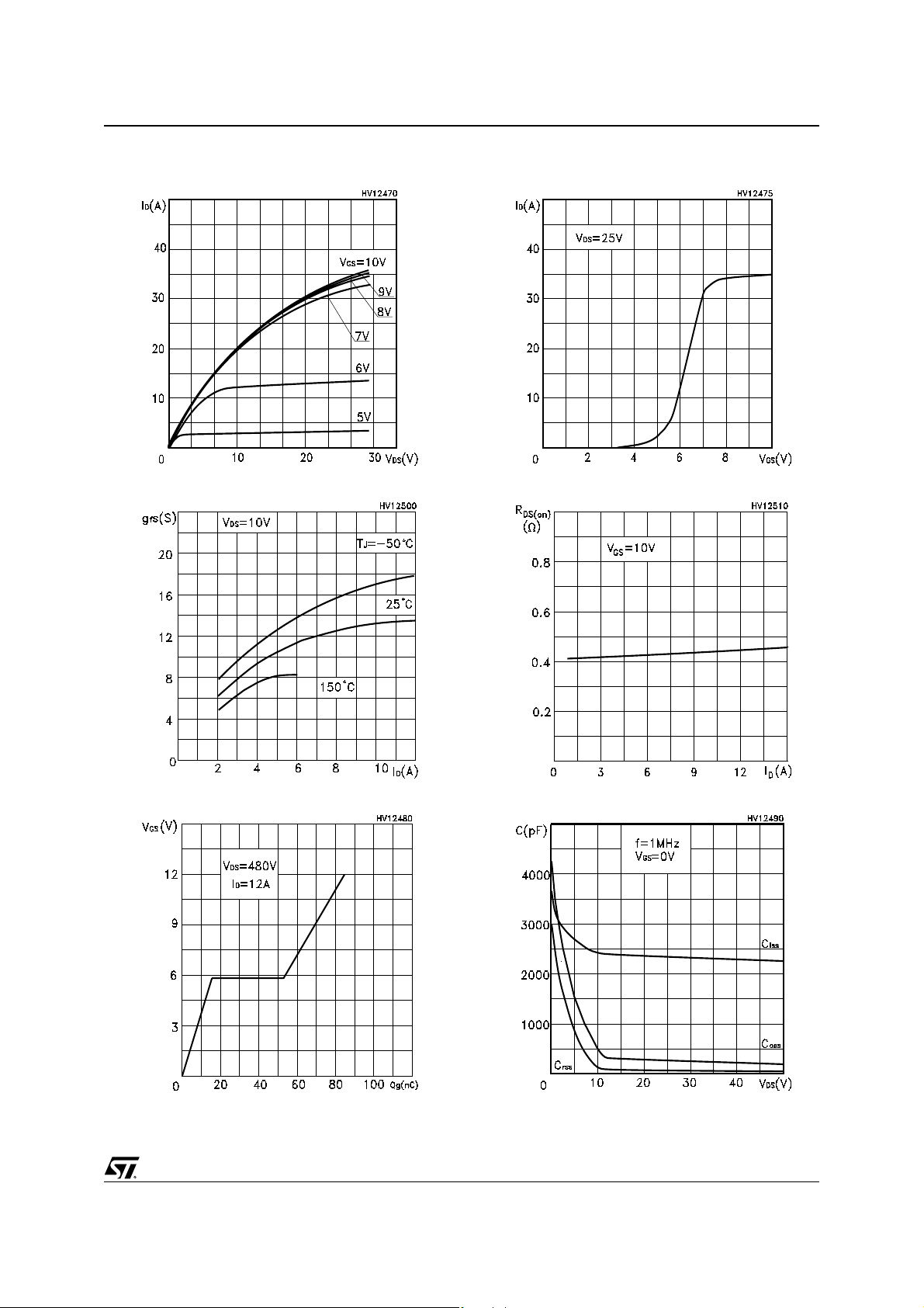
Figure 9: Output Characteristics
Figure 10: Transconductance
Figure 12: Transfer Characteristics
Figure 13: Static Drain-source On Resistance
Figure 11: Gate Charge vs Gate-source Voltage
Figure 14: Capacitance Variations
5/17
STP14NK60Z - STP14NK60ZFP - STB14NK60Z - STB14NK60Z-1 - STW14NK60Z
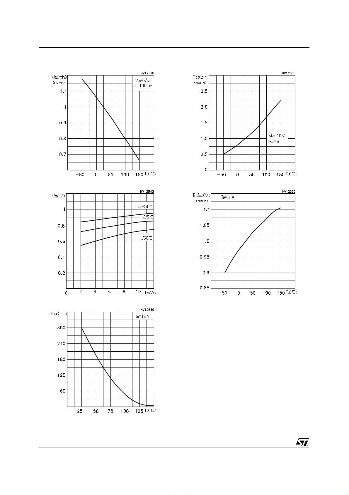
Figure 15: Normalized Gate Thereshold Voltage vs Temperature
Figure 16: Source-Drain Forwa rd Characteristics
Figure 18: Normalized On Resistance vs Temperature
Figure 19: Normalized BV
vs Temperature
DSS
Figure 17: Maximum Avalanche Energy vs
Temperature
6/17
 Loading...