


查询STB12NK80Z供应商
N-CHANNEL 800V - 0.65Ω - 10.5A - TO220-D²PAK-TO247
STB12NK80Z
STP12NK80Z - STW12NK80Z
Zener-Protected SuperMESH™ MOSFET
General features
Type
STB12NK80Z
STP12NK80Z
STW12NK80Z
■ EXTREMELY HIGH dv/dt CAPABILITY
■ IMPROVED ESD CAPABILITY
■ 100% AVALANCHE TESTED
■ GATE CHARGE MINIMIZED
■ VERY LOW INTRINSIC CAPACITANCES
■ VERY GOOD MANUFACTURI N G
V
DSSRDS(on)
800 V
800 V
800 V
<0.75 Ω
<0.75 Ω
<0.75 Ω
REPEABILITY
I
D
10.5 A
10.5 A
10.5 A
Pw
190 W
190 W
190 W
Description
The SuperMESH™ series is obtained through an
extreme optimization of ST’s well established
strip-based PowerMESH™ layout. In addition to
pushing on-resistance significantly down, spec ial
care is taken to ensure a very good dv/dt
capability for the most demanding applications.
Package
3
2
1
TO-220
D²PAK
3
1
TO-247
Internal schematic diagram
3
2
1
Applications
■ HIGH CURRENT, HIGH SPEED SWITCHING
■ IDEAL FOR OFF-LINE POWER SUPPLIES,
ADAPTOR AND PFC
Order codes
Sales Type Marking Package Packagin g
STB12NK80ZT4 B12NK80Z D²PAK TAPE & REEL
STP12NK80Z P12NK80Z TO-220 TUBE
STW12NK80Z W12NK80Z TO-247 TUBE
Rev 2
September 2005 1/15
www.st.com
15

1 Electrical ratings STB12NK80Z - STP12NK80Z - STW12NK80Z
1 Electrical ratings
Table 1. Absolute maximum ratings
Symbol Parameter Value Unit
I
DM
V
DS
V
DGR
V
GS
I
D
I
D
Note 2
P
TOT
Drain-Source Voltage (VGS = 0)
Drain-gate Voltage (RGS = 20kΩ)
800 V
800 V
Gate-Source Voltage ± 30 V
Drain Current (continuous) at TC = 25°C
Drain Current (continuous) at TC = 100°C
10.5 A
6.6 A
Drain Current (pulsed ) 42 A
Total Dis sipation at TC = 25°C
190 W
Derating Factor 1.51 W/°C
Vesd(G-S) G-S ESD (HBM C=100pF, R=1.5kΩ) 6000 V
dv/dt
Note 1
T
T
stg
Peak Diode Recovery voltage slope 4.5 V/ns
Operating Junction Temperature
j
Storage Temperature
-55 to 150 °C
Table 2. Thermal data
TO-220/D²PAK TO-247 Unit
Rthj-case Thermal Resistance Junction-case Max 0.66 °C/W
Rthj-amb Thermal Resist ance Junction- am b Max 62.5 50 °C/W
T
l
Maximum Lead Temperature For Soldering
Purpose
300 °C
Table 3. Avalanche characteristics
Symbol Parameter Max Valu e Unit
I
AR
E
AS
2/15
Avalanche Curren t, repetitive or
Not-Repetitive (pul se width l imited by Tj max)
Single Pulse Avalanche Energy
(starting Tj=25°C, I
D=IAR
, VDD= 50V)
10.5 A
400 mJ

STB12NK80Z - STP12NK80Z - STW12NK80Z 2 Electrical characteristics
2 Electrical characteristics
(T
= 25 °C unless otherwise specified)
CASE
Table 4. On/off states
Symbol Parameter Test Conditions Min. Typ. Max. Unit
V
(BR)DSS
I
DSS
I
GSS
V
GS(th)
R
DS(on)
Drain-Source Breakdown
Voltage
Zero Gate Voltage Drain
Current (V
GS
= 0)
Gate Body Leakage Current
= 0)
(V
DS
Gate Threshold Voltage
St ati c Drai n-Source On
Resistance
I
= 1mA, VGS= 0
D
= Max Ra ting,
V
DS
V
= Max Rating,Tc = 125°C
DS
= ±20V
V
GS
= VGS, ID = 100 µA
V
DS
V
= 10 V, ID= 4.5 A
GS
800 V
1
50
±10 µA
33.754.5V
0.65 0.75 Ω
Table 5. Dynamic
Symbol Parameter Test Conditions Min. Typ. Max. Unit
g
Note 4
fs
C
iss
C
oss
C
rss
C
oss eq.
Note 5
Q
Q
gs
Q
gd
Forward Transconductance
Input Capacitance
Outp u t C a pacita nce
Rev er se Trans fer Capacita n ce
Equivalent Ouput Capacitance
g
Total Gate Charge
Gate-Source Charge
Gate-Drain Charge
V
=15V, ID = 5.25A
DS
=25V, f=1 MHz, VGS=0
V
DS
=0, V
V
GS
=640V, ID = 10.5 A
V
DD
=10V
V
GS
=0V to 640V
DS
(see Figure 17)
12 S
2620
250
53
100 pF
87
14
44
µA
µA
pF
pF
pF
nC
nC
nC
Table 6. Switching times
Symbol Parameter Test Conditions Min. Typ. Max. Unit
=400 V, ID=5.25 A,
V
t
d(on)
t
t
d(off)
t
t
r(Voff)
t
t
Tur n-on Delay Time
r
Rise Time
Turn-off Delay Time
f
Fall Ti me
Off-vol tage Rise Ti me
f
c
Fall Ti me
Cross-over T ime
DD
R
=4.7Ω, VGS=10V
G
(see Figure 18)
=400 V, ID=5.25A,
V
DD
R
=4.7Ω, VGS=10V
G
(see Figure 18)
=640 V, ID=10.5A,
V
DD
R
=4.7Ω, VGS=10V
G
(see Figure 18)
30
18
70
20
16
15
28
ns
ns
ns
ns
ns
ns
ns
3/15

2 Electric al characteristics STB12NK80Z - STP12NK80Z - STW12NK80Z
Table 7. Source drain diode
Symbol Parameter Test Conditions Min. Typ. Max. Unit
I
SDM
V
SD
I
I
SD
Note 2
Note 4
t
rr
Q
rr
RRM
Source-drain Current
Source-drain Current (pulsed)
Forward on Voltage
Reverse Recovery Time
Reverse Recovery Charge
Reverse Recovery Current
ISD=10.5 A, VGS=0
=10.5A, di/dt = 100A/µs,
I
SD
V
=100 V, Tj=150°C
DD
10.5
42
1.6 V
635
5.9
18.5
Table 8. Gate-source zener diode
Symbol Parameter Test Conditions Min. Ty p. Max. Unit
BV
GSO
Note 6
(1) ISD ≤10.5 A, di/dt ≤200A/µs, VDD ≤ V
(2) Pul s e width limited by safe operat ing area
(3) Limited only by maximu m temperat ure allowed
(4) Pulsed: pulse duration = 300µs, duty cycle 1.5%
(5) C
oss eq.
to 80%V
(6)The built-in back-to-back Zener diodes have specifically been designed to enhance not only the device’s ESD capability, but
also to make them safely absorb possible voltage transients that may occasionally be applied from gate to source. In this
respect the Zener voltage is appropriate to achieve an efficient and cost-effective intervention to protect the device’s
integrity. Th ese integrated Z ener diodes thus avoid the usage of external components.
Gate-Source
Breakdown Voltage
is defined as a constant equivalent capacitance giving the same charging time as C
DSS
Igs=±1mA
(Open Drain)
, Tj ≤ T
(BR)DSS
JMAX
30 V
when VDS increases from 0
oss
A
A
ns
µC
A
4/15

STB12NK80Z - STP12NK80Z - STW12NK80Z 2 Electrical characteristics
2.1 Electrical Characteristics (curves)
Figure 1. Safe Ope ra tin g A rea for
TO-220/D²PAK
Figure 3. Safe Operating Area for TO-247 Figure 4. Thermal Impedance for TO-247
Figure 2. Thermal Im pedanc e for
TO-220/D²PAK
Figure 5. Output Characteristics Figure 6. Transfer Characteristics
5/15

2 Electric al characteristics STB12NK80Z - STP12NK80Z - STW12NK80Z
Figure 7. Transconductance Figure 8. S tatic Drain-Source on Resistance
Figure 9. Gate Charge vs Gate -Source
Voltage
Figure 10. Normalized Gate Threshold Volta ge
vs Temperatute
Figure 11. Capacitance Variations
Figure 12. Normalized on Resistance vs
Temperature
6/15

STB12NK80Z - STP12NK80Z - STW12NK80Z 2 Electrical characteristics
Figure 13. Source-drain Diode Forward
Characteristics
Figure 15. Maximum Avalanche Energy vs
Temperature
Figure 14. Norma lized BVDSS vs Temperature
7/15

3 Test circuits STB12NK80Z - STP12NK80Z - STW12NK80Z
3 Test circuits
Figure 16. Switching Times Test Circuit For
Resistive Load
Figure 18. Test Circuit For Indictive Load
Switching and Diode Recovery
Times
Figure 17. Gate Charge Test Circuit
Figure 20. Unclamped Inductive Load Test
Circuit
Figure 19. Unclamped Inductive Waveform
8/15

STB12NK80Z - STP12NK80Z - STW12NK80Z 4 Package mechani cal data
4 P ack age mechanical data
In order to meet environmental requirements, ST offers these devices in ECOPACK®
packages. These packages have a Lead-free second level interconnect . The category of
second level interconnect is marked on the package and on the inner box label, in compliance
with JEDEC Standard JESD97. The maximum ratings related to soldering conditions are also
marked on the inner box label. ECOPACK is an ST trademark. ECOP ACK specifications are
available at: www.st.com
9/15

4 Package mechani cal data STB12NK80Z - STP12NK80Z - STW12NK80Z
TO-220 MECHANICAL DATA
DIM.
A 4.40 4.60 0.173 0.181
b 0.61 0.88 0.024 0.034
b1 1.15 1.70 0.045 0.066
c 0.49 0.70 0.019 0.027
D 15.25 15.75 0.60 0.620
E 10 10.40 0.393 0.409
e 2.40 2.70 0.094 0.106
e1 4.95 5.15 0.194 0.202
F 1.23 1.32 0.048 0.052
H1 6.20 6.60 0.244 0.256
J1 2.40 2.72 0.094 0.107
L 13 14 0.511 0.551
L1 3.50 3.93 0.137 0.154
L20 16.40 0.645
L30 28.90 1.137
øP 3.75 3.85 0.147 0.151
Q 2.65 2.95 0.104 0.116
MIN. TYP MAX. MIN. TYP. MAX.
mm. inch
10/15
STB12NK80Z - STP12NK80Z - STW12NK80Z 4 Package mechani cal data
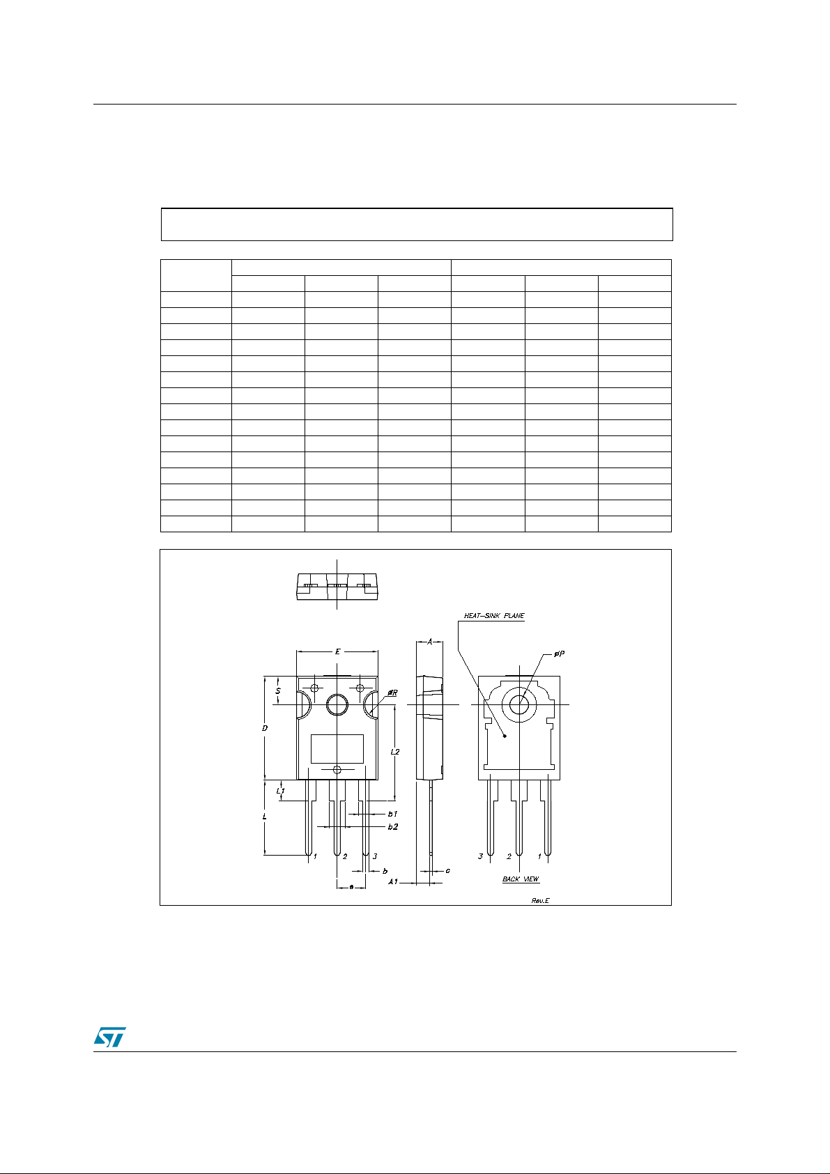
TO-247 MECHANICAL DATA
DIM.
A 4.85 5.15 0.19 0.20
A1 2.20 2.60 0.086 0.102
b 1.0 1.40 0.039 0.055
b1 2.0 2.40 0.079 0.094
b2 3.0 3.40 0.118 0.134
c 0.40 0.80 0.015 0.03
D 19.85 20.15 0.781 0.793
E 15.45 15.75 0.608 0.620
e5.45 0.214
L 14.20 14.80 0.560 0.582
L1 3.70 4.30 0.14 0.17
L2 18.50 0.728
øP 3.55 3.65 0.140 0.143
øR 4.50 5.50 0.177 0.216
S5.50 0.216
MIN. TYP MAX. MIN. TYP. MAX.
mm. inch
11/15

4 Package mechani cal data STB12NK80Z - STP12NK80Z - STW12NK80Z
D2PAK MECHANICAL DATA
TO-247 MECHANICAL DATA
DIM.
A 4.4 4.6 0.173 0.181
A1 2.49 2.69 0.098 0.106
A2 0.03 0.23 0.001 0.009
B 0.7 0.93 0.027 0.036
B2 1.14 1.7 0.044 0.067
C 0.45 0.6 0.017 0.023
C2 1.23 1.36 0.048 0.053
D 8.95 9.35 0.352 0.368
D1 8 0.315
E 10 10.4 0.393
E1 8.5 0.334
G 4.88 5.28 0.192 0.208
L 15 15.85 0.590 0.625
L2 1.27 1.4 0.050 0.055
L3 1.4 1.75 0.055 0.068
M 2.4 3.2 0.094 0.126
R0.4 0.015
V2 0º 4º
MIN. TYP MAX. MIN. TYP. MAX.
mm. inch
3
12/15
1

STB12NK80Z - STP12NK80Z - STW12NK80Z 5 Packing mechanical data
5 Packing mechanical data
D2PAK FOOTPRINT
TAPE AND REEL SHIPMENT
REEL MECHANICAL DATA
DIM.
A 330 12.992
B 1.5 0.059
C 12.8 13.2 0.504 0.520
D 20.2 0795
G 24.4 26.4 0.960 1.039
N 100 3.937
T 30.4 1.197
mm inch
MIN. MAX . MIN. MAX.
T APE MECHANICAL DATA
DIM.
A0 10.5 10.7 0.413 0.421
B0 15.7 15.9 0.618 0.626
D 1.5 1.6 0.059 0.063
D1 1.59 1.61 0.062 0.063
E 1.65 1.85 0.065 0.073
F 11.4 11.6 0.449 0.456
K0 4.8 5.0 0.189 0.197
P0 3.9 4.1 0.153 0.161
P1 11.9 12.1 0.468 0.476
P2 1.9 2.1 0.075 0.082
R 50 1.574
T 0.25 0.35 0.0098 0.0137
W 23.7 24.3 0.933 0.956
* on sales type
mm inch
MIN. MAX. MIN. MAX.
BASE QTY BULK QTY
1000 1000
13/15

6 Revision Hist ory STB12NK80Z - STP12NK80Z - STW12NK80Z
6 R evi sion History
Date Revision Changes
02-Sep-2005 2 Inserted Ecopack indication
14/15

STB12NK80Z - STP12NK80Z - STW12NK80Z 6 Revision History
Information furnished is believed to be accurate and reliable. However, STMicroelectronics assumes no responsibility for the consequences
of use of such information nor for any infringement of patents or other rights of third parties which may result from its use. No license is granted
by implic ation or oth erwise under any patent or pat ent rights of STMicroelectron i cs . Specifications mentioned in th i s publication are sub je ct
to change without notice. This publication supersedes and replaces all information previously supplied. STMicroelectronics products are not
authoriz ed for use as crit ic al components in life support devices or systems without express written appr oval of STMicroelectronics.
The ST logo is a registered trademark of ST M i croelectr onics.
All other nam es are the pro perty of their respective owners
© 2005 STMi croelectro ni cs - All rights reserved
STMicroelectronic s group of companies
Austra l i a - Be l gi um - Brazil - C anada - China - Czech Republic - Finland - F rance - Germany - Hong Kon g - India - Israe l - It al y - Japan -
Malaysi a - M al ta - Morocco - Singapore - Spain - Swede n - Switzerland - United Kingdom - United States of America
www.st.com
15/15
 Loading...