

1
3
3
查询STMAV340供应商
STripFET™ III Power MOSFET for DC-DC Conversion
General features
STB120NH03L
STP120NH03L
N-Channel 30V - 0.005Ω - 9A - TO-220/D2PAK
Type
STB120NH03L
STP120NH03L
■ Typical R
■ R
■ Conduction Losses Reduced
■ Switching Losses Reduced
■ Low Threshold Device
*Qg Industry’s Benchmark Low
DS(on)
V
DSS
30V
30V
= 0.005Ω @ 10V
DS(on)
R
DS(on)
<0.0055Ω
<0.0055Ω
I
D
9A Note 1
9A Note 1
Description
These devices utilizes the latest advanced design
rules of ST’s proprietary STripFET™ technology.
It is ideal in high performanc e DC-DC converter
applications where efficiency is to be achieved at
very high output currents.
Applications
■ Specifically designed and optimized for high
efficiency DC-DC converters
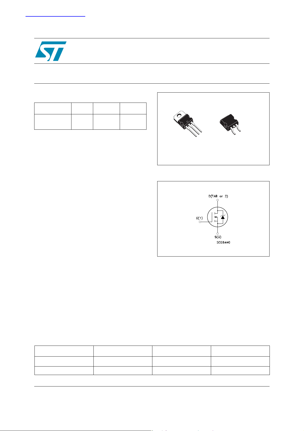
2
TO-220
1
D2PAK
Internal schematic diagram
Order codes
Part Number Marking Package Packaging
STB120NH03L B120NH03L
STP120NH03L P120NH03L TO-220 TUBE
December 2005 1/14
2
D
PAK
TAPE & REEL
Rev 1
www.st.com
14

1 Electrical ratings STB120NH03L - STP120NH03L
1 Electrical ratings
Table 1. Absolute maximum ratings
Symbol Parameter Value Unit
V
DS
V
DGR
V
GS
ID Note 1 Drain Current (continuous) at TC = 25°C
I
Note 1 Drain Current (continuous) at TC = 100°C
D
Note 2
I
DM
P
TOT
Drain-source Voltage (V
Drain-gate Voltage (R
GS
GS
= 0V)
= 20kΩ)
30 V
30 V
Gate-Source Voltage ± 20 V
60 A
60 A
Drain Current (pulsed ) 240 A
Total Dissip ation at TC = 25°C
115 W
Derating Factor 0.77 W/°C
EAS Note 3 Single Pulse Avalanche Energy 700 mJ
T
J
T
stg
Operating Junction Temperature
Storage Temperature
-55 to 175 °C
Table 2. Thermal data
R
R
thJC
thJA
T
Thermal Resist ance Junction-case Max 1.30 °C/W
Thermal Resist ance Junction-amb Max 62.5 °C/W
Maximum Lead Temperature For Soldering
l
Purpose
300 °C
2/14
STB120NH03L - STP120NH03L 2 Electrical characteristics
2 Electrical characteristics
( T
= 25 °C unless otherwise specified )
CASE
Table 3. On/off states
Symbol Parameter Test Conditions Min. Typ. Max. Unit
V
(BR)DSS
I
DSS
I
GSS
V
GS(th)
R
DS(on)
Drain-Source Breakdown
Voltage
Zero Gate Voltage Drain
Current (V
GS
= 0)
Gate Body Leakage Current
= 0)
(V
DS
Gate Threshold Voltage
St ati c Drai n-Source On
Resistance
I
= 250μA VGS= 0
D
= Max Ra ting,
V
DS
= Max Ra ting,TC=125°C
V
DS
= ±20V
V
GS
= VGS ID = 250µA
V
DS
V
= 10V ID = 30A
GS
V
= 5V ID = 30A
GS
30 V
1
10
±100 µA
11.82.5V
0.005
0.006
0.0055
0.0105
Table 4. Dynamic
Symbol Parameter Test Conditions Min. Typ. Max. Unit
g
fs
C
C
C
Note 4
iss
oss
rss
Forward Transconductance
Input Capacitance
Outp u t C a pacitanc e
Rev er se Transf er Capac it a n ce
Rg Gate Input Resistance
V
= 10V ID = 30A
DS
= 15V, f = 1MHz, V
V
DS
GS
f = 1MHz Gate DC Bias=0
Test Signal Level=20mV
Open Drain
= 0
40 S
4100
680
70
1.3 Ω
µA
µA
Ω
Ω
pF
pF
pF
Qoss
Qgls
Q
g
Q
gs
Q
gd
Note 5
Note 6
Total Gate Charge
Gate-Source Charge
Gate-Drain Charge
Output Charge
Third-quadrant Gate Charge
=15V, ID = 60A
V
DD
=10V
V
GS
Figure 14 on page 7
V
= 16V V
DS
V
< 0 VGS= 10V
DS
GS
= 0
57
77
11.8
7.3
27 ns
55 ns
nC
nC
nC
3/14

2 Electric al characteristics STB120NH03L - STP120NH03L
Table 5. Switching times
Symbol Parameter Test Conditions Min. Typ. Max. Unit
= 15V, ID = 30A,
V
t
d(on)
t
t
d(off)
Tur n- on D elay Ti me
r
Rise Time
Off volt age Rise Time
t
f
FallTime
DD
= 4.7Ω, V
R
G
GS
= 10V
Figure 13 on page 7
= 15V, ID = 30A,
V
DD
= 4.7Ω, V
R
G
GS
= 10V
Figure 15 on page 7
16
95
48
23
ns
ns
ns
ns
Table 6. Sour ce dr ai n di ode
Symbol Parameter Test Conditions Min. Typ. Max. Unit
V
SD
I
SD
I
SDM
Note 4
t
rr
Q
rr
I
RRM
Source-drain Current
Source-drain Current (pulsed)
Forward on Voltage
Reverse Recovery Time
Reverse Recovery Charge
Reverse Recovery Current
I
I
V
Figure 15 on page 7
Note: 1 Value limited by wire bonding
2 Pulse width limited by safe operating area
3 Starting T
= 25°C , ID = 30A, VDD = 15V
J
4 Pulsed: pulse duration = 300µs, duty cycle 1.5%
5Q
oss
= C
*Δ VIN, C
oss
= Cgd + Cds. See Power losses calculation
oss
6 Gate charge for synchronous operation.
= 30A V
SD
= 60A, di/dt = 100A/µs,
SD
= 30V, TJ =150°C
DD
GS
= 0
46
64
2.8
60
240
1.4 V
A
A
ns
nC
A
4/14
STB120NH03L - STP120NH03L 2 Electrical characteristics
2.1 Electrical chraracteristics (curves)
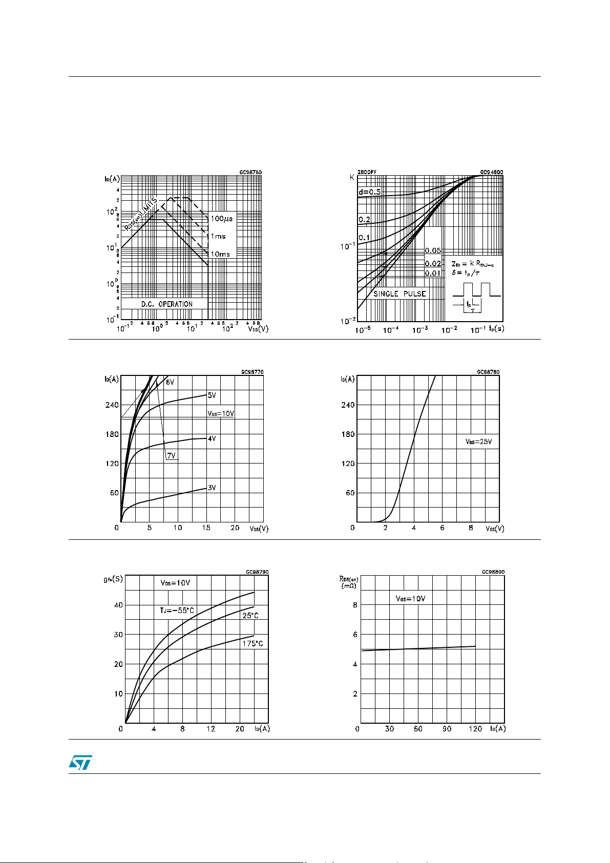
Figure 1. Safe Operating Area Figure 2. Thermal Impedance
Figure 3. Output Characteristics Figure 4. Transfer Characteristics
Figure 5. Transconductance Figure 6. Static Drain-Source on Resistance
5/14

2 Electric al characteristics STB120NH03L - STP120NH03L
Figure 7. Gate Charge vs Gate-Source Voltage Figure 8. Capacitance Variations
Figure 9. Normalized Gate Threshold Volt ag e
vs Temperature
Figure 11. Source-drain Diode Forward
Characteristics
Figure 10. Normalized on Resistance vs
Temperature
Figure 12. Normalized Breakdown Vo l tage vs
Temperature
6/14

STB120NH03L - STP120NH03L 3 Test circuits
3 Test circuits
Figure 13. Switching Times Test Circuit For
Resistive Load
Figure 15. Test Circuit For Inductive Load
Switching and Diode Recovery
Times
Figure 14. Gate Charge Test Circuit
Figure 17. Unclamped Inductive Load Test
Circuit
Figure 16. Unclamped Inductive Waveform
7/14

4 Package mechani cal data STB120NH03L - STP120NH03L
4 P ack age mechanical da ta
In order to meet environmental requirements, ST offers these devices in ECOPACK®
packages. These packages have a Lead-free second level interconnect . The category of
second level interconnect is marked on the package and on the inner box label, in compliance
with JEDEC Standard JESD97. The maximum ratings related to soldering conditions are also
marked on the inner box label. ECOPACK is an ST trademark. ECOPACK specifications are
available at: www.st.com
8/14

STB120NH03L - STP120NH03L 4 Package mechanical data
Table 7. TO-220 Mechanical Data
Dimensions
Ref.
Min. Typ. Max. Min. Typ. Max.
A 4.40 4.60 0.173 0.181
b 0.61 0.88 0.024 0.035
b1 1.15 1.70 0.045 0.067
c 0.49 0.70 0.019 0.028
D 15.25 15.75 0.600 0.620
E 10.0 10.40 0.394 0.409
e 2.4 2.7 0.094 0.106
e1 4.95 5.15 0.195 0.203
F 1.23 1.32 0.048 0.052
H1 6.2 6.6 0.244 0.260
J1 2.40 2.72 0.094 0.107
L 13.0 14.0 0.512 0.551
L1 3.5 3.93 0.138 0.155
L20 16.4 0.646
L30 28.9 1.138
öP 3.75 3.85 0.148 0.152
Q 2.65 2.95 0.104 0.116
mm inch
Figure 18. TO-220 Package Dimension
9/14

4 Package mechani cal data STB120NH03L - STP120NH03L
Table 8. D2PAK Mechanical Data
Dimensions
mm inch
Ref.
A 4.4 4.6 0.173 0.181
A1 2.49 2.69 0.098 0.106
A2 0.03 0.23 0.001 0.009
B 0.7 0.93 0.028 0.037
B2 1.14 1.7 0.045 0.067
C 0.45 0.6 0.018 0.024
C2 1.21 1.36 0.048 0.054
D 8.95 9.35 0.352 0.368
D1 8 0.315
E 10 10.4 0.394 0.409
E1 8.5 0.334
G 4.88 5.28 0.192 0.208
L 15 15.85 0.591 0.624
L2 1.27 1.4 0.050 0.055
L3 1.4 1.75 0.055 0.069
M 2.4 3.2 0.094 0.126
R 0.4 0.015
V2 0° 8° 0° 8°
Min. Typ. Max. Min. Typ. Max.
Figure 19. D2PAK Package Dimensions
10/14

STB120NH03L - STP120NH03L 5 Appendix A
5 Appendix A
Figure 20. Buck Converter: Power Losses Estimation
The power losses associated with the FETs in a Synchronous Buck converter can be estimated
using the equations shown in the table below. The formulas give a good approximation, for the
sake of performance comparison, of how different pairs of devices affect the converter
efficiency. However a very important parameter, the working temperature, is not considered.
The real device behavior is really dependent on how the heat generated inside the devices is
removed to allow for a safer working junction temperature.
The low side (SW2) device requires:
● Ver y low R
● Small Qgls to reduce the gate charge losses
● Small Coss to reduce losses due to output capacitance
● Small Qrr to reduce losses on SW1 during its turn-on
● The Cgd/Cgs ratio lower than Vth/Vgg ratio especially with low drain to source
● voltage to avoid the cross conduction phenomenon;
to reduce conduction losses
DS(on)
The high side (SW1) device requires:
● Small Rg and Ls to allow higher gate current peak and to limit the voltage feedback on the
gate
● Small Qg to have a faster commutation and to reduce gate charge losses
● Low R
to reduce the conduction losses.
DS(on)
11/14

5 Appendix A STB120NH03L - STP120NH03L
R
)
R
V
f
V
f
V
f
Q
f
Q
2
f
2
f
Table 9. Power losses calculation
High Side Switching (SW1) Low Side Switch (SW2)
Pconduction
Pswitching Zero Voltage Switching
Recovery
(1)
Pdiode
Conduction Not applicable
Pgate(Q
1. Dissipated by SW1 during turn-on
P
Qoss
)
G
Table 10. Paramiters meaning
2
LDS(on)SW1
+
gd(SW1)gsth(SW1)in
Not applicable
ggg(SW1)
oss(SW1)in
2
1(*I *
δ
δ
*I *
I
L
*f*)Q(Q*
I
g
rr(SW2)in
*V*
*Q*V
oss(SW2)in
−
LDS(on)SW2
*Q*
*t*I*
deadtimeLf(SW2)
*V*
gggls(SW2)
*Q*V
Parameter Meaning
d Duty-cycle
Q
gsth
Q
gls
Pconduction On state los ses
Pswitching On-off transition losses
Pdiode Conduction and rever se recovery diode losses
Pgate Gate drive losses
P
Qoss
Post threshold gate charge
Third quadrant gate charge
Output capacitance losses
12/14

STB120NH03L - STP120NH03L 6 Revision History
6 R evi sion History
Date Revision Description of changes
12-Dec-2005 1 First release
13/14

6 Revision Hist ory STB120NH03L - STP120NH03L
I
s
o
d
b
ct
t
ot
a
nformation furnished is believed to be accurate and reliable. However, STMicroelectronics assumes no responsibility for the consequence
f use of such information nor for any infringement of patents or other rights of third parties which may result from its use. No license is grante
y implic ation or otherwise under any patent or patent righ ts of STMicroelectronics. Sp ecifications mentioned in this publicati on are subje
o change without notice. This publication supersedes and replaces all information previously supplied. STMicroelectronics products are n
uthoriz ed for use as critical components in l i fe support devices or systems without express wr i tt en approval of STMi croelectron ics.
The ST logo is a registered tra dem ark of STMicroe l ectronics.
All other nam es are the prope rty of their respective owners
© 2005 STMi croelectronics - All rights res erved
Austra l i a - Be l gi um - Brazil - Canada - China - Czech Republic - Finl and - France - Germ any - Hong Kong - In di a - Israel - Italy - Japan -
Malaysi a - M al ta - Morocco - Singapore - Spain - S weden - Switze rl and - United Kingdom - United States of America
STMicroelectronics group of companies
www.st.com
14/14
 Loading...