


STB120NF10
STP120NF10
N-CHANNEL 100V - 0.009 Ω - 120A D²PAK/TO-220
STripFET™ II POWER MOSFET
TYPE
STB120NF10
STP120NF10
■ TYPICAL R
■ EXCEPTIONA L dv/d t CAPABILITY
■ 100% AVALANCHE TESTED
■ APPLICATION ORIENTED
V
DSS
100 V
100 V
(on) = 0.009 Ω
DS
R
DS(on)
< 0.0105
< 0.0105
I
D
120 A
Ω
120 A
Ω
CHARACTERIZATION
■ SURFACE-MOUNTING D²PAK (TO-263)
POWER PACKAGE IN TAPE & REEL
(SUFFIX “T4")
DESCRIPTION
This MOSFET series realized with STMicroelectronics
unique STripFET process has specifically been designed
to minimize the on-resistance. It is therefore suitable as
primary switch in advanced high-efficiency, highfrequency isolated DC-DC converters for Telecom and
Computer applications. It is also intended for any
applications with low gate drive requirements.
APPLICATIONS
■ AUDIO AMPLI FIERS
■ POWER TOOLS
3
1
D2PAK
TO-263
(Suffix “T4”)
TO-220
INTERNAL SCHEMATIC DIAGRAM
3
2
1
Ordering Information
STB120NF10
STP120NF10
SALES TYPE MARKING PACKAGE PACKAGING
B120NF10
P120NF10
TO-263
TO-220
T APE & REEL
TUBE
ABSOLUTE MAXIMUM RATINGS
Symbol Parameter Value Unit
V
DS
V
DGR
V
GS
I
D
I
D
(
I
DM
P
tot
dv/dt
E
AS
T
stg
T
j
(
Pulse width l i mited by safe operating area. (1) ISD ≤120A, di/dt ≤300A/µs, VDD ≤ V
•)
Drain-source Voltage (VGS = 0)
Drain-gate Voltage (RGS = 20 kΩ)
100 V
100 V
Gate- source Voltage ± 20 V
Drain Current (continuous) at TC = 25°C
Drain Current (continuous) at TC = 100°C
•)
Drain Current (pulsed) 480 A
Total Dissipation at TC = 25°C
120 A
85 A
312 W
Derating Factor 2.08 W/°C
(1)
Peak Diode Recovery voltage slope 10 V/ns
(2)
Single Pulse Avalanche Energy 550 mJ
Storage Temperature
Operating Junction Temperature
(2) Starting Tj = 25 oC, ID = 60A, VDD = 50V
-55 to 175 °C
(BR)DSS
, Tj ≤ T
JMAX
1/10May 2003
STB120NF10 STP120NF10
THERMA L D ATA
Rthj-case
Rthj-amb
T
Thermal Resistance Junction-case
Thermal Resistance Junction-ambient
Maximum Lead Temperature For Soldering Purpose
l
Max
Max
0.48
62.5
300
°C/W
°C/W
°C
ELECTRICAL CHARACTERISTICS (T
= 25 °C UNLESS OTHERWISE SPECIFIED)
CASE
OFF
Symbol Parameter Test Conditions Min. Typ. Max. Unit
= 250 µA, VGS = 0
V
(BR)DSS
Drain-source
I
D
100 V
Breakdown Voltage
= Max Rating
V
DS
V
= Max Rating TC = 125°C
DS
V
= ± 20 V
GS
1
10
±100 nA
ON
(*)
I
DSS
I
GSS
Zero Gate Voltage
Drain Current (V
GS
Gate-body Leakage
Current (V
DS
= 0)
= 0)
Symbol Parameter Test Conditions Min. Typ. Max. Unit
V
GS(th)
R
DS(on)
Gate Threshold Voltage
Static Drain-source On
= VGS I
DS
V
= 10 V ID = 60 A
GS
= 250 µA
D
24V
0.009 0.0105
V
Resistance
DYNAMIC
Symbol Parameter Test Conditions Min. Typ. Max. Unit
(*)
g
fs
C
iss
C
oss
C
rss
Forward Transconductance
Input Capacitance
Output Capacitance
Reverse Transfer
Capacitance
V
15 V
V
DS =
DS
ID
= 25V f = 1 MHz VGS = 0
= 60 A
TBD S
5200
785
325
µA
µA
Ω
pF
pF
pF
2/10
STB120NF10 STP120NF10
ELECTRICAL CHARACTERISTICS (continued)
SWITCHING ON
Symbol Parameter Test Conditions Min. Typ. Max. Unit
= 50 V ID = 60 A
t
d(on)
Turn-on Delay Time
t
r
Rise Time
V
DD
R
= 4.7 Ω VGS = 10 V
G
(Resistive Load, Figure 3)
Q
g
Q
gs
Q
gd
Total Gate Charge
Gate-Source Charge
Gate-Drain Charge
=80 V ID=120 A VGS=10 V
V
DD
SWITCHING OFF
Symbol Parameter Test Conditions Min. Typ. Max. Unit
= 50 V ID = 60 A
t
d(off)
Turn-off Delay Time
t
f
Fall Time
V
DD
R
= 4.7Ω, V
G
GS
= 10 V
(Resistive Load, Figure 3)
SOURCE DRAIN DIODE
Symbol Parameter Test Conditions Min. Typ. Max. Unit
I
SD
I
SDM
V
SD
t
rr
Q
rr
I
RRM
(*)
Pulsed: P ul se duration = 300 µs, duty cycle 1.5 %.
(
Pulse widt h l i m i ted by safe operating area.
•)
Source-drain Current
(•)
Source-drain Current (pulsed)
(*)
Forward On Voltage
Reverse Recovery Time
Reverse Recovery Charge
Reverse Recovery Current
I
= 120 A VGS = 0
SD
= 120 A di/dt = 100A/µs
I
SD
V
= 40 V Tj = 150°C
DD
(see test circuit, Figure 5)
25
90
172
32
64
132
68
152
760
10
233 nC
120
480
1.3 V
ns
ns
nC
nC
ns
ns
A
A
ns
nC
A
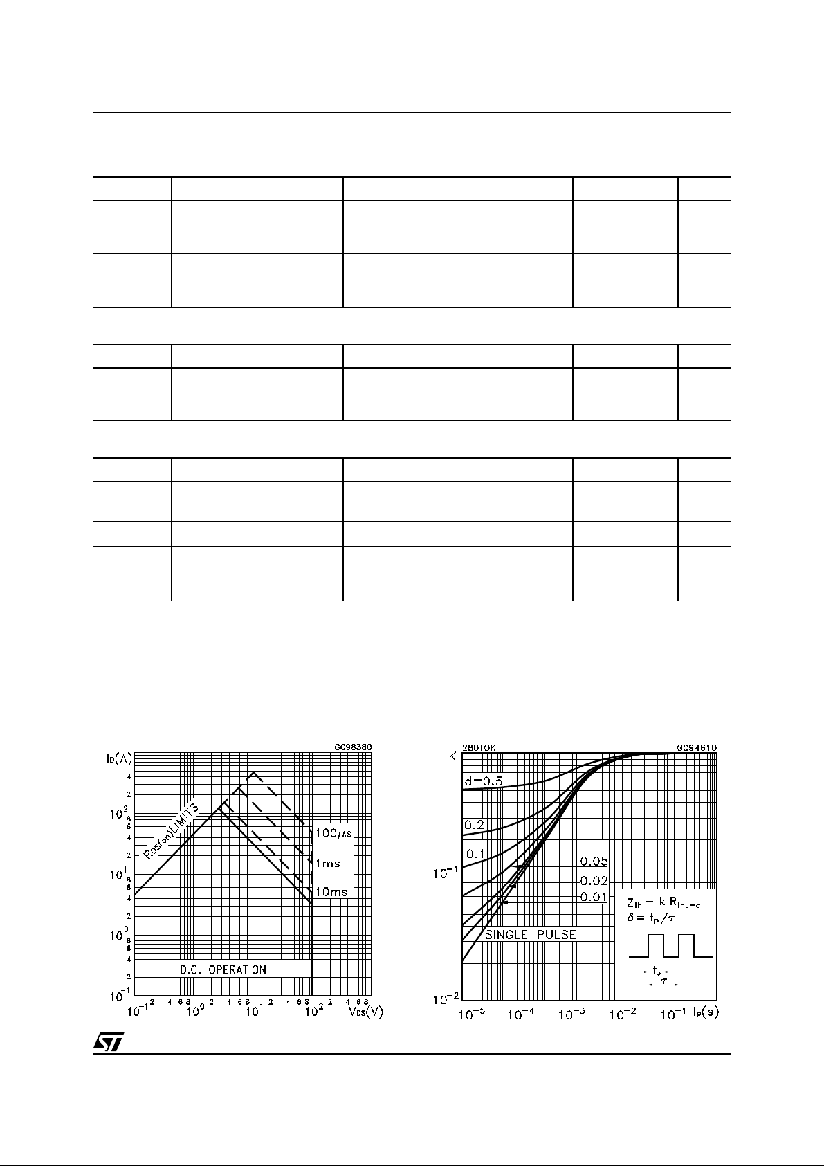
Safe Operating Area Thermal Impedance
3/10
STB120NF10 STP120NF10
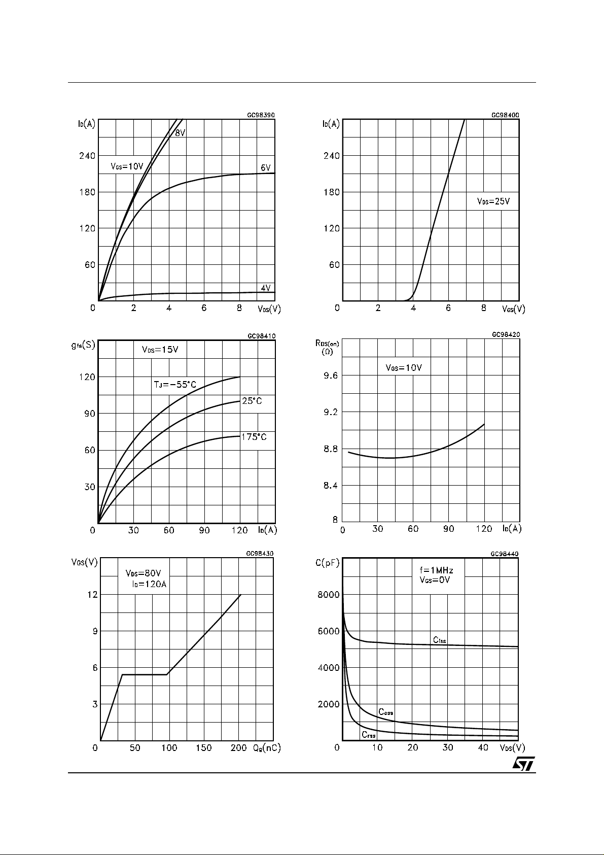
Output Characteristics Transfer Characteristics
Transconductance Static Drain-source On Resistance
Gate Charge vs Gate-source Voltage Capacitance Variations
4/10
 Loading...