

Page 1
STP11NM80 - STF11NM80
STB11NM80 - STW11NM80
N-CHANNEL 800V - 0.35 Ω - 11 A TO-220 /FP/D2PAK/TO-247
MDmesh™ MOSFET
Tabl e 1 : General Feat ures
TYPE V
STP11NM80
STF11NM80
STB11NM80
STW11NM80
■ TYPICA L R
■ LOW GATE INPUT RESISTANCE
■ LOW INPUT CAPACITANCE AND GATE
DSSRDS(on)RDS(on)*QgID
800 V
800 V
800 V
800 V
DS
< 0.40 Ω
< 0.40 Ω
< 0.40 Ω
< 0.40 Ω
(on) = 0.35 Ω
14 Ω∗nC
14 Ω∗nC
14 Ω∗nC
14 Ω∗nC
11 A
11 A
11 A
11 A
CHARGE
■ BEST R
(on)*Qg IN THE INDUSTRY
DS
DESCRIPTION
The MDmesh™ associates the Multiple Drain process with the Company’s PowerMesh™ horizontal
layout assuring an oustanding low on-resistance.
The adoption of the Company’s proprietary strip
technique yields overall dynamic performance that
is significantly better than that of similar compe tition’s products.
APPLICATIONS
The 800 V MDmes h™ family is very suitable for
single swit ch a pplicat ion s in part icula r for Fl yba ck
and Forward converter topologies and for ignition
circuits in the field of lighting.
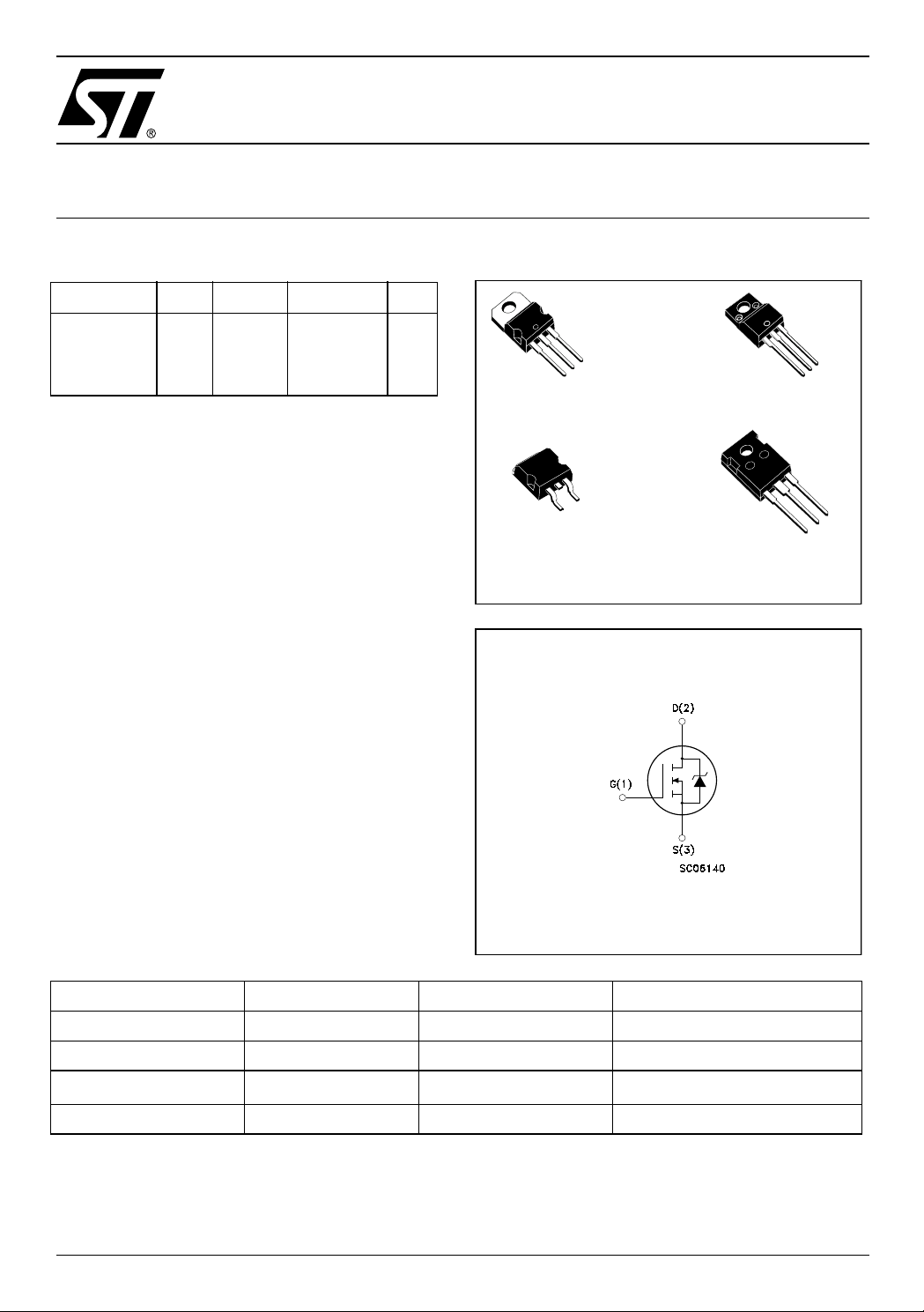
Figure 1: Package
3
2
1
TO-220
2
PAK
D
3
1
TO-220FP
TO-247
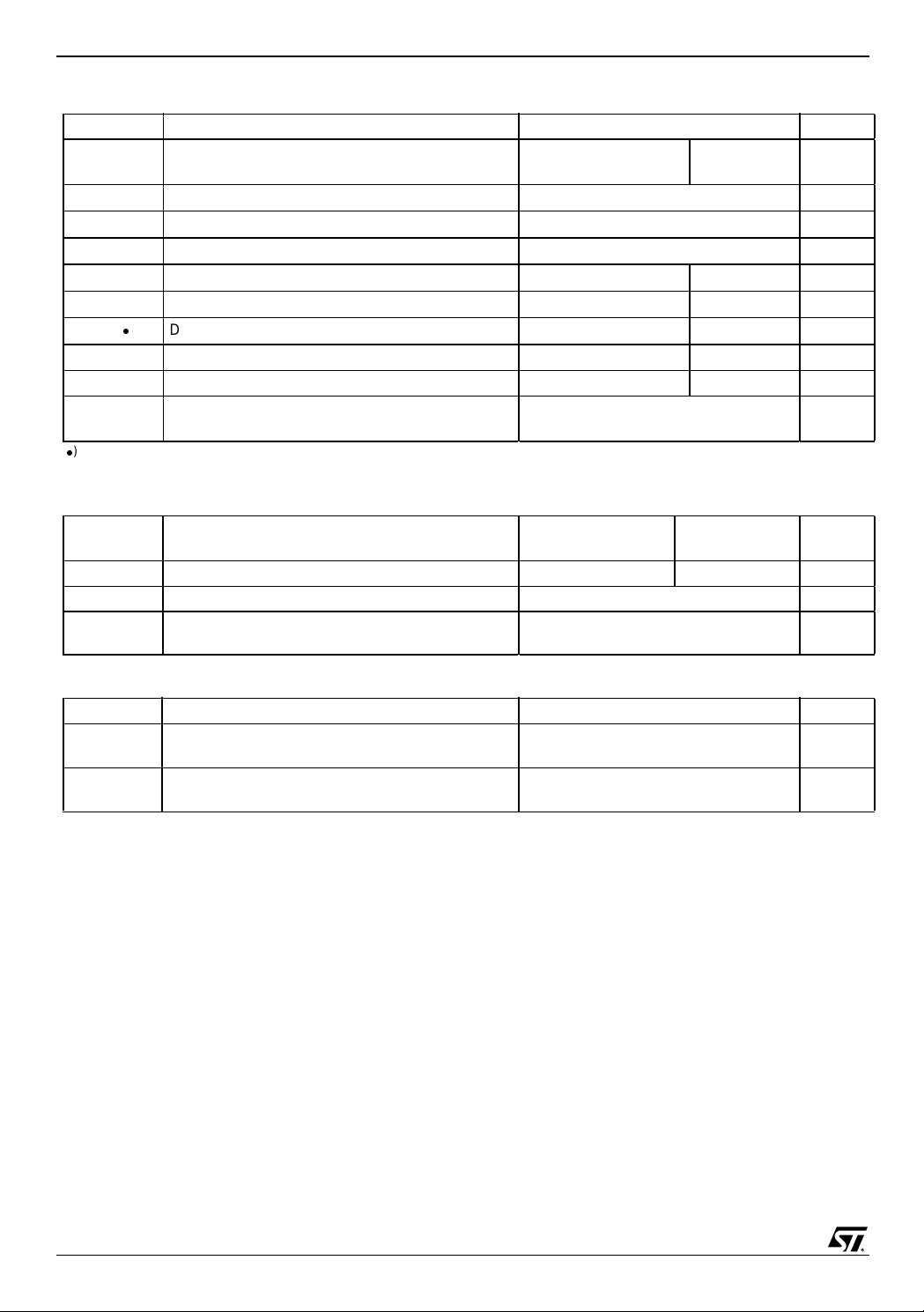
Figure 2: Internal Schematic Diagram
3
2
1
3
2
1
Table 2: Order Codes
SALES TYPE MARKING PACKAGE PACKAGING
STP11NM80 P11NM80 TO-220 TUBE
STF11NM80 F11NM80 TO-220FP TUBE
STB11NM80T4
STW11NM80 W11NM80 TO-247 TUBE
B11NM80
2
D
PAK
TAPE & REEL
Rev. 2
1/14September 2004
Page 2
STP11NM8O - STF11NM80 - STB11N M 80 - STW11NM80
Table 3: Absolute Maximum ratings
Symbol Parameter Value Unit
2
TO-220/D
V
I
DM
P
V
DGR
V
I
I
TOT
DS
GS
D
D
Drain-source Voltage (VGS = 0)
Drain-gate Voltage (RGS = 20 kΩ)
Gate- source Voltage ± 30 V
Drain Current (continuous) at TC = 25°C
Drain Current (continuous) at TC = 100°C
()
Drain Current (pulsed) 44
Total Dissipation at TC = 25°C
Derating Factor 1.2 0.28 W /°C
T
j
T
stg
(
) Pulse width l i m i t ed by safe oper at i ng area
(*) Limit ed only by the Maximum Te mperature All owed
Operating Junction Temperature
Storage Temperature
Table 4: Thermal Data
TO-220/D
TO-247
Rthj-case Thermal Resistance Junction-case Max 0.83 3.6 °C/W
Rthj-amb Thermal Resistance Junction-ambient Max 62.5 °C/W
T
l
Maximum Lead Temperature For Soldering
Purpose
PAK
TO-247
TO-220FP
800 V
800 V
11
4.7
11 (*)
4.7 (*)
44 (*)
150
35
-65 to 150 °C
2
PAK
TO-220FP Unit
300 °C
A
A
A
W
Table 5: Avalanche Characteristics
Symbol Parameter Max Value Unit
I
AR
E
AS
Avalanche Current, Repetitive or Not-Repetitive
(pulse width limited by T
max)
j
Single Pulse Avalanche Energy
(starting T
= 25 °C, ID = 2.5A, VDD = 50 V)
j
2.5 A
400 mJ
2/14
Page 3

STP11NM8O - STF11NM80 - STB11NM80 - STW11NM80
ELECTRICAL CHARACTERISTICS (T
=25°C UNLESS OTHERWISE SPECIFIED)
CASE
Table 6: On/Off
Symbol Parameter Test Conditions Min. Typ. Max. Unit
V
(BR)DSS
Drain-source
ID = 250 µA, VGS = 0 800 V
Breakdown Voltage
I
DSS
I
GSS
V
GS(th)
R
DS(on)
Zero Gate Voltage
Drain Current (V
GS
= 0)
Gate-body Leaka ge
Current (V
DS
= 0)
Gate Threshold Voltage
Static Drain-source On
V
= Max Rating
DS
V
= Max Rating, TC = 125 °C
DS
V
= ± 30V 100 nA
GS
V
= VGS, ID = 250 µA
DS
345V
10
100
VGS = 10V, ID =5.5 A 0.35 0.40 Ω
Resistance
Table 7: Dynamic
Symbol Parameter Test Conditions Min. Typ. Max. Unit
g
(1) Forward Transconductance VDS > I
fs
C
C
C
R
t
d(on)
t
d(off)
Q
Q
Q
iss
oss
rss
t
r
t
f
gs
gd
G
g
Input Capacitance
Output Capacitance
Reverse Transfer
Capacitance
Gate Input Resistance f=1 MHz Gate DC Bias = 0
Turn-on Delay Time
Rise Time
Turn-off Delay Time
Fall Time
Total Gate Charge
Gate-Source Charge
Gate-Drain Charge
ID = 7.5 A
V
DS
Test Signal Level = 20mV
Open Drain
V
DD
RG=4.7Ω VGS = 10 V
(Resistive Load see, Figure 4)
V
DD
VGS = 10V
D(on)
x R
DS(on)max,
8S
= 25 V, f = 1 MHz, VGS = 0 1630
750
30
2.7 Ω
= 400 V, ID = 5.5 A
22
17
46
15
= 640 V, ID = 11 A,
43.6
11.6
21
µA
µA
pF
pF
pF
ns
ns
ns
ns
nC
nC
nC
Table 8: Source Drain Diode
Symbol Parameter Test Conditions Min. Typ. Max. Unit
I
SD
I
(2)
SDM
(1)
V
SD
t
rr
Q
rr
I
RRM
t
rr
Q
rr
I
RRM
Note: 1. Pulsed: P ul se duration = 300 µs, duty cycle 1.5 % .
2. Pulse wi dt h l i m ited by safe op erating area.
Source-drain Current
Source-drain Current (pulsed)
Forward On Voltage
Reverse Recovery Time
Reverse Recovery Charge
Reverse Recovery Current
Reverse Recovery Time
Reverse Recovery Charge
Reverse Recovery Current
ISD = 11 A, VGS = 0
I
SD
V
DD
(see test circuit, Figure 5)
I
SD
V
DD
(see test circuit, Figure 5)
= 11 A, di/dt = 100 A/µs
= 50 V, Tj = 25°C
= 11 A, di/dt = 100 A/µs
= 50 V, Tj = 150°C
612
7.22
23.6
970
11.25
23.2
11
44
0.86 V
A
A
ns
µC
A
ns
µC
A
3/14
Page 4
STP11NM8O - STF11NM80 - STB11N M 80 - STW11NM80
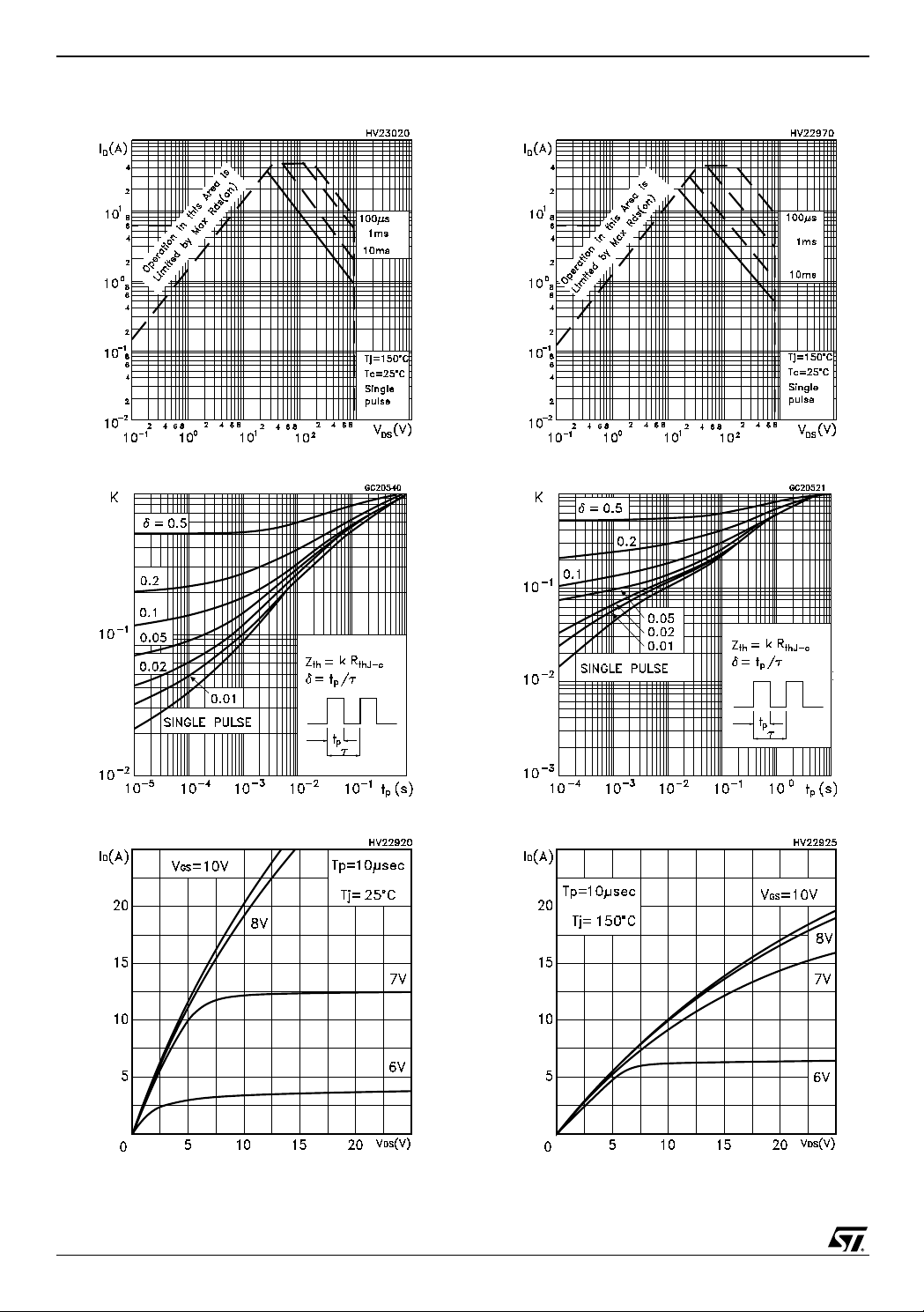
Figure 3: Safe Operating Area For D2PAK/ TO-247 / TO-220
Figure 4: Thermal Impedance For D
2
PAK/
TO-247 / TO-220
Figure 6: Safe Operating Area For TO-220FP
Figure 7: Thermal Impedance For TO-220FP
Figure 5: Output Characteristics
4/14
Figure 8: Output Characteristics
Page 5
STP11NM8O - STF11NM80 - STB11NM80 - STW11NM80
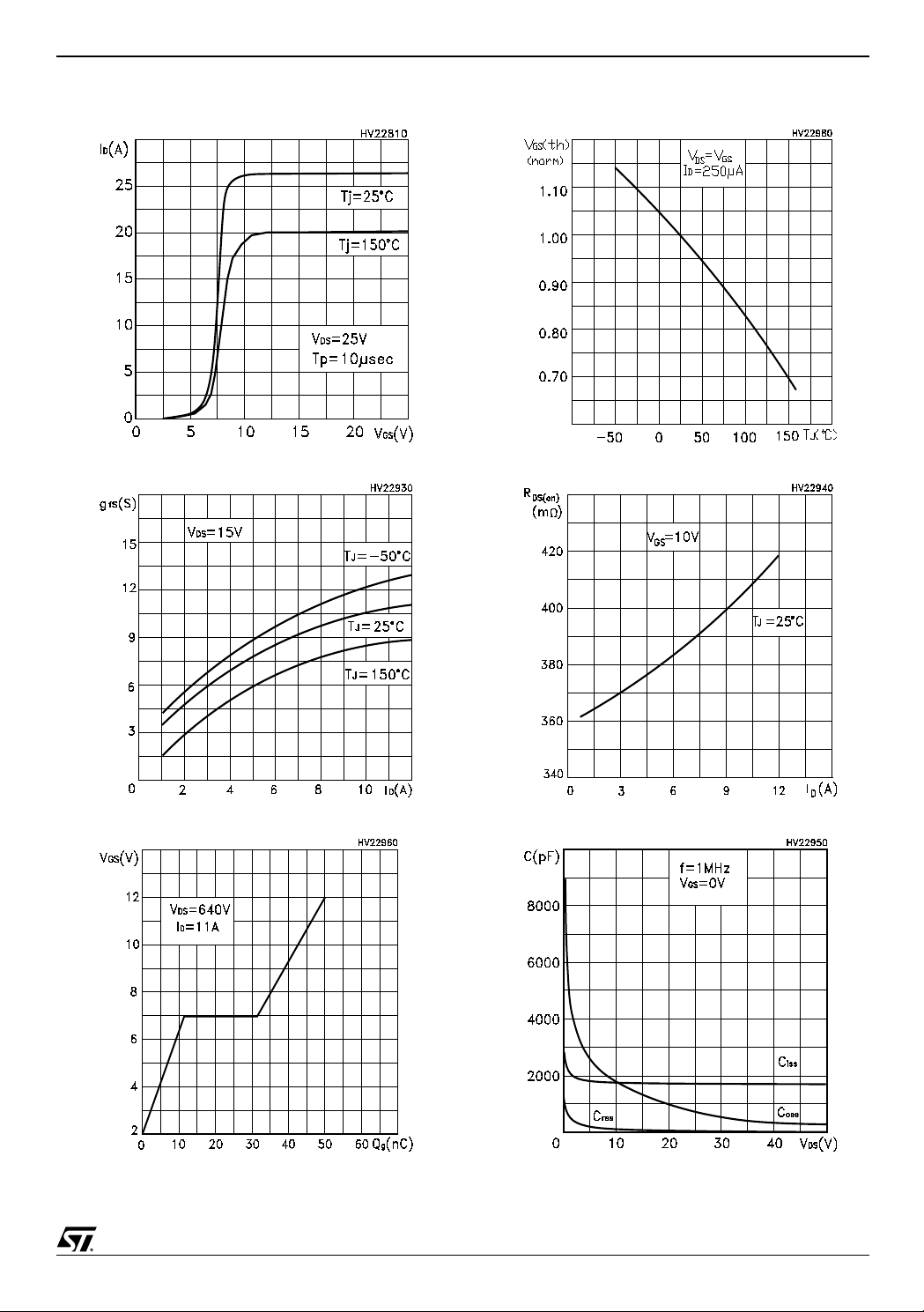
Figure 9: Transfer Characteristics
Figure 10: Transconductance
Figure 12: Normalized Gate Threshold Voltage vs Tem perature
Figure 13: Static Drain-Source On Resistance
Figure 11: Gate Charge vs Gate-source Voltage
Figure 14: Capacitance Variations
5/14
Page 6

STP11NM8O - STF11NM80 - STB11N M 80 - STW11NM80
Figure 15: Norm alized O n Resis tance vs T emperature
Figure 16: S ource-Drain Forward Char acteristics
Figure 17: Normalized BV
vs Temperature
DSS
6/14
Page 7

STP11NM8O - STF11NM80 - STB11NM80 - STW11NM80
Figure 18: Unclamped Inductive Load Test Circuit
Figure 19: Switching Times Test Circuit For Resistive Load
Figure 21: Unclamped Inductive Wafeform
Figure 22: Gate Charge Test Circuit
Figure 20: Test Circuit For Inductive Load Switching and Diode Recovery Times
7/14
Page 8

STP11NM8O - STF11NM80 - STB11N M 80 - STW11NM80
TO-220 MECHANICAL DATA
DIM.
A 4.40 4.60 0.173 0.181
b 0.61 0.88 0.024 0.034
b1 1.15 1.70 0.045 0.066
c 0.49 0.70 0.019 0.027
D 15.25 15.75 0.60 0.620
E 10 10.40 0.393 0.409
e 2.40 2.70 0.094 0.106
e1 4.95 5.15 0.194 0.202
F 1.23 1.32 0.048 0.052
H1 6.20 6.60 0.244 0.256
J1 2.40 2.72 0.094 0.107
L 13 14 0.511 0.551
L1 3.50 3.93 0.137 0.154
L20 16.40 0.645
L30 28.90 1.137
øP 3.75 3.85 0.147 0.151
Q 2.65 2.95 0.104 0.116
MIN. TYP MAX. MIN. TYP. MAX.
mm. inch
8/14
Page 9

STP11NM8O - STF11NM80 - STB11NM80 - STW11NM80
TO-220FP MECHANICAL DATA
DIM.
A 4.4 4.6 0.173 0.181
B 2.5 2.7 0.098 0.106
D 2.5 2.75 0.098 0.108
E 0.45 0.7 0.017 0.027
F 0.75 1 0.030 0.039
F1 1.15 1.7 0.045 0.067
F2 1.15 1.7 0.045 0.067
G 4.95 5.2 0.195 0.204
G1 2.4 2.7 0.094 0.106
H 10 10.4 0.393 0.409
L2 16 0.630
L3 28.6 30.6 1.126 1.204
L4 9.8 10.6 .0385 0.417
L5 2.9 3.6 0.114 0.141
L6 15.9 16.4 0.626 0.645
L7 9 9.3 0.354 0.366
Ø 3 3.2 0.118 0.126
MIN. TYP MAX. MIN. TYP. MAX.
mm. inch
E
A
D
B
L3
L6
L7
F1
F
G1
H
F2
123
L4
L2
L5
G
9/14
Page 10

STP11NM8O - STF11NM80 - STB11N M 80 - STW11NM80
TO-263 (D2PAK) MECHANICAL DATA
DIM.
A 4.32 4.57 0.178 0.180
A1 0.00 0.25 0.00 0.009
b 0.71 0.91 0.028 0.350
b2 1.15 1.40 0.045 0.055
c 0.46 0.61 0.018 0.024
c2 1.22 1.40 0.048 0.055
D 8.89 9.02 9.40 0.350 0.355 0.370
D1 8.01 0.315
E 10.04 10.28 0.395 0.404
e 2.54 0.010
H 13.10 13.70 0.515 0.540
L 1.30 1.70 0.051 0.067
L1 1.15 1.39 0.045 0.054
L2 1.27 1.77 0.050 0.069
L4 2.70 3.10 0.106 0.122
V2 0° 8° 0°
MIN. TYP MAX. MIN. TYP. MAX.
mm. inch
8°
10/14
Page 11

STP11NM8O - STF11NM80 - STB11NM80 - STW11NM80
TO-247 MECHANICAL DATA
DIM.
A 4.85 5.15 0.19 0.20
A1 2.20 2.60 0.086 0.102
b 1.0 1.40 0.039 0.055
b1 2.0 2.40 0.079 0.094
b2 3.0 3.40 0.118 0.134
c 0.40 0.80 0.015 0.03
D 19.85 20.15 0.781 0.793
E 15.45 15.75 0.608 0.620
e5.45 0.214
L 14.20 14.80 0.560 0.582
L1 3.70 4.30 0.14 0.17
L2 18.50 0.728
øP 3.55 3.65 0.140 0.143
øR 4.50 5.50 0.177 0.216
S5.50 0.216
MIN. TYP M AX. MIN. TYP. MAX.
mm. inch
11/14
Page 12

STP11NM8O - STF11NM80 - STB11N M 80 - STW11NM80
D2PAK FOOTPRINT
TAPE AND REEL SHIPMENT (suffix ”T4”)*
TUBE SHIPMENT (no suffix)*
REEL MECHANICAL DATA
DIM.
A 330 12.992
B 1.5 0.059
C 12.8 13.2 0.504 0.520
D 20.2 0795
G 24.4 26.4 0.960 1.039
N 100 3.937
T 30.4 1.197
mm inch
MIN. MAX. MIN. MAX.
T APE MECHANICAL DATA
DIM.
A0 10.5 10.7 0.413 0.421
B0 15.7 15.9 0.618 0.626
D 1.5 1.6 0.059 0.063
D1 1.59 1.61 0.062 0.063
E 1.65 1.85 0.065 0.073
F 11.4 11.6 0.449 0.456
K0 4.8 5.0 0.189 0.197
P0 3.9 4.1 0.153 0.161
P1 11.9 12.1 0.468 0.476
P2 1.9 2.1 0.075 0.082
R 50 1.574
T 0.25 0.35 0.0098 0.0137
W 23.7 24.3 0.933 0.956
* on sales type
mm inch
MIN. MAX. MIN. MAX.
BASE QTY BULK QTY
1000 1000
12/14
Page 13

STP11NM8O - STF11NM80 - STB11NM80 - STW11NM80
Figure 23: Revision History
Date Revision Description of Change s
29-Jul-2004 1 Final Document
13/14
Page 14

STP11NM8O - STF11NM80 - STB11N M 80 - STW11NM80
Information furnished is believed to be accurate and reliable. However, STMicroelectronics assumes no responsibility for the consequences
of use of s uch inf ormati on nor for a ny infr ing eme nt o f p atent s or o ther ri ghts of third parties whic h m ay r esul t from i ts use. No license is gran ted
by implication or otherwise under any patent or patent rights of STMicroelectronics. Specifications mentioned in this publication are subject
to change without notice. This publication supersedes and replaces all information previously suppl ied. STMicroelectronics products are not
authorized for use as critical components in life support devices or systems without express written approval of STMicroelectronics.
The ST logo is a registered trademark of STMicroelectronics
All other names are the property of their respective owners
© 2004 STMicroelectronics - All Rights Reserved
STMicroelectronics group of companies
Australia - Belgium - Brazil - Canada - China - Czech Republic - Finland - France - Germany - Hong Kong - India - Israel - Italy - Japan -
Malaysia - Malta - Morocco - Singapore - Spain - Sweden - Switzerland - United Kingdom - United States of America
14/14
 Loading...