

查询STB100NF03L-03-01供应商
STB100NF03L-03 STP100NF03L-03
N-CHANNEL 30V - 0.0026 Ω -100A D²PAK/I²PAK/TO-220
STB100NF03L-03-1
STripFET™ II POWER MOSFET
TYPE
STB100NF03L-03
STP100NF03L-03
STB100NF03L-03-01
■ TYPICAL R
■ LOW THRESHOLD DRIVE
■ 100% AVALANCHE TESTED
■ LOGIC LEVEL DEVICE
■ THROUGH-HOLE IPAK (TO-251) POWER
DS
V
DSS
30 V
30 V
30 V
(on) = 0.0026 Ω
R
DS(on)
<0.0032
<0.0032
<0.0032
I
D
100 A
Ω
100 A
Ω
100 A
Ω
PACKAGE IN TUBE (SUFFIX “- 1 ")
■ SURFACE-MOUNTING D
2
PAK (TO-263)
POWER PACKAG E IN TU BE (NO SU FFIX) OR
IN TAPE & REEL (SUFFIX “T4”)
DESCRIPTION
This Power MOSFET is the latest dev elo pment of
STMicroelectronis unique "Single Feature Size™"
strip-based process. The resulting transistor
shows extremely high packing density for low onresistance, rugged avalanche characteristics and
less critical alignment steps therefore a remarkable manufacturing reproducibility.
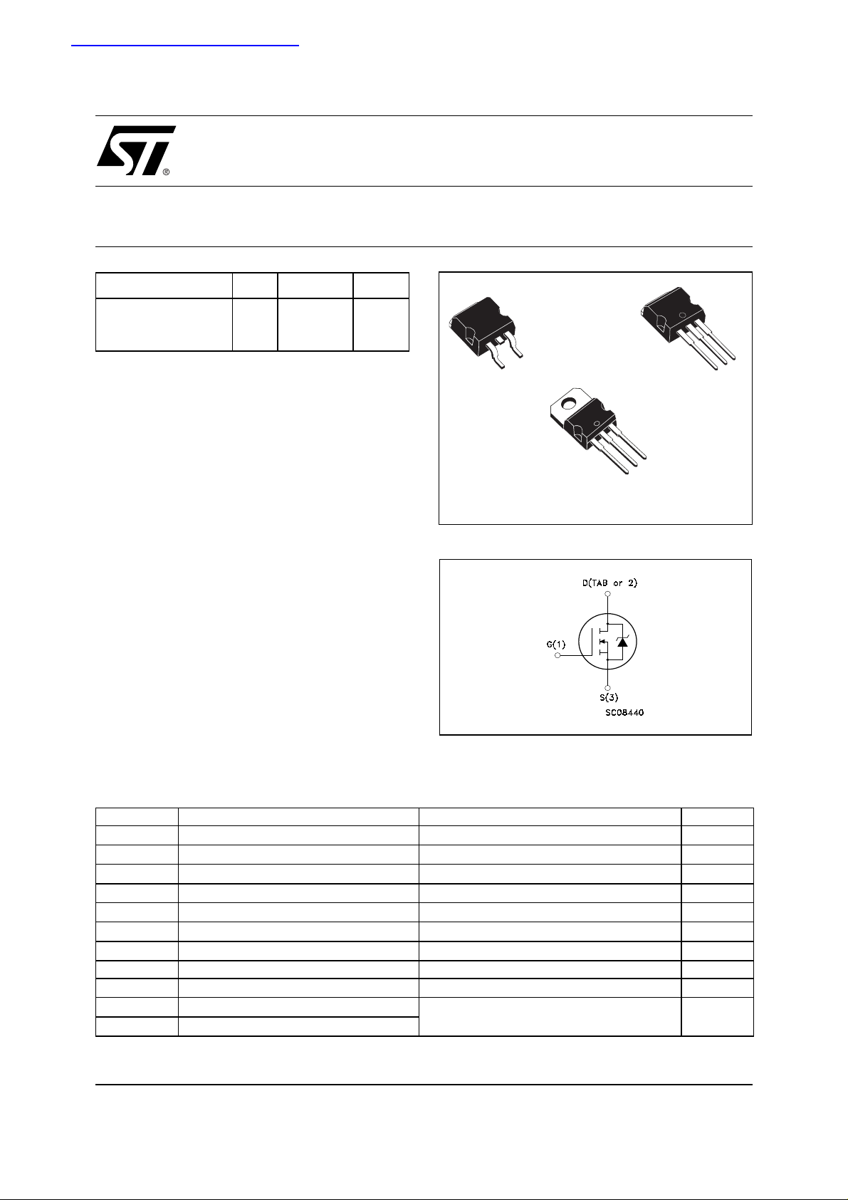
3
1
D2PAK
TO-263
(Suffix “T4”)
3
2
1
TO-220
INTERNAL SCHEMATIC DIAGRAM
1
I2PAK
TO-262
(Suffix “-1”)
3
2
APPLICATIONS
■ HIGH CURRENT, HIGH SWITCHING SPEED
■ MOTOR CONTROL, AUDIO AMPLIFIERS
■ DC-DC & DC-AC CONVERTERS
■ SOLENOID AND RELAY DRIVERS
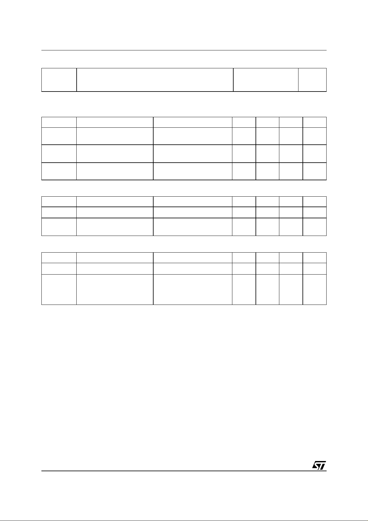
ABSOLUTE MAXIMUM RATINGS
Symbol Parameter Value Unit
V
DS
V
DGR
V
GS
I
(1) Drain Current (continuous) at T
D
(1) Drain Current (continuous) at T
I
D
(
I
DM
P
tot
E
AS
T
stg
T
j
(
Pulse widt h l i m i ted by safe operating area
•)
(1) Current Limited by Package
.
Drain-source Voltage (VGS = 0)
Drain-gate Voltage (RGS = 20 kΩ)
30 V
30 V
Gate- source Voltage ± 16 V
= 25°C
C
= 100°C
C
•)
Drain Current (pulsed) 400 A
Total Dissipation at TC = 25°C
100 A
100 A
300 W
Derating Factor 2 W/°C
(2)
Single Pulse Avalanche Energy 1.9 J
Storage Temperature
Operating Junction Temperature
(2) Starting Tj = 25 oC, IAR = 50A, VDD = 50V
-55 to 175 °C
1/11February 2003
STB100NF03L-03 STP100NF03L-03 STB100NF03L-03-1
THERMA L D ATA
Rthj-case
Rthj-amb
T
l
Thermal Resistance Junction-case
Thermal Resistance Junction-ambient
Maximum Lead Temperature For Soldering Purpose
Max
Max
0.5
62.5
300
°C/W
°C/W
°C
ELECTRICAL CHARACTERISTICS (T
= 25 °C unless otherwise specified)
case
OFF
Symbol Parameter Test Conditions Min. Typ. Max. Unit
= 250 µA, VGS = 0
V
(BR)DSS
Drain-source
I
D
30 V
Breakdown Voltage
= Max Rating
V
DS
= Max Rating TC = 125°C
V
DS
= ± 16V
V
GS
1
10
±100 nA
ON
(*)
I
DSS
I
GSS
Zero Gate Voltage
Drain Current (V
GS
Gate-body Leakage
Current (V
DS
= 0)
= 0)
Symbol Parameter Test Conditions Min. Typ. Max. Unit
V
V
GS(th)
R
DS(on)
Gate Threshold Voltage
Static Drain-source On
Resistance
= V
DS
GS
= 10 V ID = 50 A
V
GS
= 4.5 V ID = 50 A
V
GS
ID = 250 µA
1 1.7 2.5 V
0.0026
0.0032
0.0032
0.0045
DYNAMIC
Symbol Parameter Test Conditions Min. Typ. Max. Unit
(*)
g
fs
C
iss
C
oss
C
rss
Forward Transconductance
Input Capacitance
Output Capacitance
Reverse Transfer
Capacitance
VDS>I
D(on)xRDS(on)max ID
= 25V f = 1 MHz VGS = 0
V
DS
=10 A
10 S
6200
1720
300
µA
µA
Ω
Ω
pF
pF
pF
2/11
STB100NF03L-03 STP100NF03L-03 STB100NF03L-03-1
ELECTRICAL CHARACTERISTICS (continued)
SWITCHING ON
Symbol Parameter Test Conditions Min. Typ. Max. Unit
= 15 V ID = 50 A
t
d(on)
Q
Q
Q
t
r
g
gs
gd
Turn-on Time
Rise Time
Total Gate Charge
Gate-Source Charge
Gate-Drain Charge
SWITCHING OFF
Symbol Parameter Test Conditions Min. Typ. Max. Unit
t
d(off)
t
t
r(Voff)
t
t
f
f
c
Turn-off Delay Time
Fall Time
Off-Voltage Rise Time
Fall Time
Cross-over Time
V
DD
= 4.7
R
Ω
G
VGS = 4.5 V
(Resistive Load, Figure 3)
= 24V ID= 100A VGS= 5V
V
DD
= 20 V ID = 50 A
V
DD
= 4.7Ω, V
R
G
GS
= 4.5 V
(Resistive Load, Figure 3)
V
= 24 V ID = 100 A
clamp
= 4.7
R
Ω
G
V
GS
= 4.5 V
(Inductive Load, Figure 5)
35
315
88
22.5
36
115
95
110
55
100
ns
ns
nC
nC
nC
ns
ns
ns
ns
ns
SOURCE DRAIN DIODE
Symbol Parameter Test Conditions Min. Typ. Max. Unit
I
SD
I
SDM
V
SD
t
rr
Q
rr
I
RRM
(*)
Pulsed: P ul se duration = 300 µs, duty cycle 1. 5 %.
(
•)Pulse width limited by saf e operating ar ea.
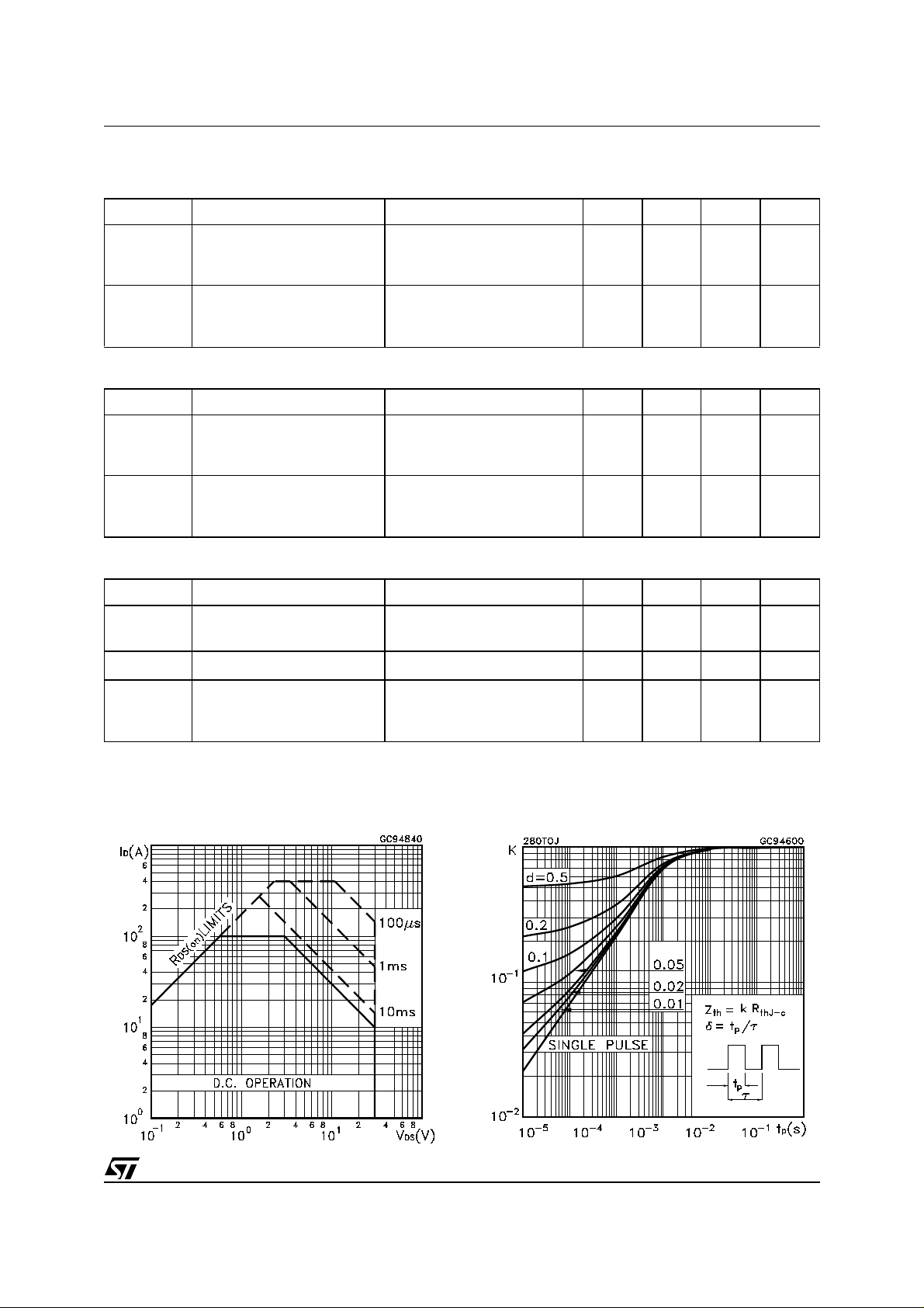
Safe Operating Area
Source-drain Current
(•)
Source-drain Current (pulsed)
(*)
Forward On Voltage
Reverse Recovery Time
Reverse Recovery Charge
Reverse Recovery Current
I
= 100 A VGS = 0
SD
= 100 A di/dt = 100A/µs
I
SD
= 20 V Tj = 150°C
V
DD
(see test circuit, Figure 5)
Thermal Impedance
100
400
1.3 V
75
150
4
A
A
ns
nC
A
3/11
STB100NF03L-03 STP100NF03L-03 STB100NF03L-03-1
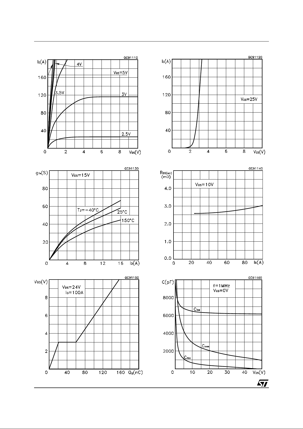
Output Characteristics Transfer Characteristics
Transconductance Static Drain-source On Resistance
Gate Charge vs Gate-source Voltage Capacitance Variations
4/11
 Loading...