

查询STB100NF03L-03-01供应商
STB100NF03L-03 STP100NF03L-03
N-CHANNEL 30V - 0.0026 Ω -100A D²PAK/I²PAK/TO-220
STB100NF03L-03-1
STripFET™ II POWER MOSFET
TYPE
STB100NF03L-03
STP100NF03L-03
STB100NF03L-03-01
■ TYPICAL R
■ LOW THRESHOLD DRIVE
■ 100% AVALANCHE TESTED
■ LOGIC LEVEL DEVICE
■ THROUGH-HOLE IPAK (TO-251) POWER
DS
V
DSS
30 V
30 V
30 V
(on) = 0.0026 Ω
R
DS(on)
<0.0032
<0.0032
<0.0032
I
D
100 A
Ω
100 A
Ω
100 A
Ω
PACKAGE IN TUBE (SUFFIX “- 1 ")
■ SURFACE-MOUNTING D
2
PAK (TO-263)
POWER PACKAG E IN TU BE (NO SU FFIX) OR
IN TAPE & REEL (SUFFIX “T4”)
DESCRIPTION
This Power MOSFET is the latest dev elo pment of
STMicroelectronis unique "Single Feature Size™"
strip-based process. The resulting transistor
shows extremely high packing density for low onresistance, rugged avalanche characteristics and
less critical alignment steps therefore a remarkable manufacturing reproducibility.
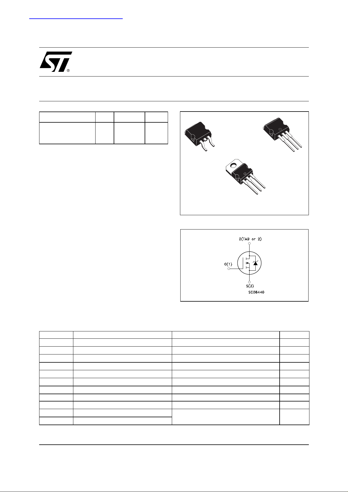
3
1
D2PAK
TO-263
(Suffix “T4”)
3
2
1
TO-220
INTERNAL SCHEMATIC DIAGRAM
1
I2PAK
TO-262
(Suffix “-1”)
3
2
APPLICATIONS
■ HIGH CURRENT, HIGH SWITCHING SPEED
■ MOTOR CONTROL, AUDIO AMPLIFIERS
■ DC-DC & DC-AC CONVERTERS
■ SOLENOID AND RELAY DRIVERS
ABSOLUTE MAXIMUM RATINGS
Symbol Parameter Value Unit
V
DS
V
DGR
V
GS
I
(1) Drain Current (continuous) at T
D
(1) Drain Current (continuous) at T
I
D
(
I
DM
P
tot
E
AS
T
stg
T
j
(
Pulse widt h l i m i ted by safe operating area
•)
(1) Current Limited by Package
.
Drain-source Voltage (VGS = 0)
Drain-gate Voltage (RGS = 20 kΩ)
30 V
30 V
Gate- source Voltage ± 16 V
= 25°C
C
= 100°C
C
•)
Drain Current (pulsed) 400 A
Total Dissipation at TC = 25°C
100 A
100 A
300 W
Derating Factor 2 W/°C
(2)
Single Pulse Avalanche Energy 1.9 J
Storage Temperature
Operating Junction Temperature
(2) Starting Tj = 25 oC, IAR = 50A, VDD = 50V
-55 to 175 °C
1/11February 2003
STB100NF03L-03 STP100NF03L-03 STB100NF03L-03-1
THERMA L D ATA
Rthj-case
Rthj-amb
T
l
Thermal Resistance Junction-case
Thermal Resistance Junction-ambient
Maximum Lead Temperature For Soldering Purpose
Max
Max
0.5
62.5
300
°C/W
°C/W
°C
ELECTRICAL CHARACTERISTICS (T
= 25 °C unless otherwise specified)
case
OFF
Symbol Parameter Test Conditions Min. Typ. Max. Unit
= 250 µA, VGS = 0
V
(BR)DSS
Drain-source
I
D
30 V
Breakdown Voltage
= Max Rating
V
DS
= Max Rating TC = 125°C
V
DS
= ± 16V
V
GS
1
10
±100 nA
ON
(*)
I
DSS
I
GSS
Zero Gate Voltage
Drain Current (V
GS
Gate-body Leakage
Current (V
DS
= 0)
= 0)
Symbol Parameter Test Conditions Min. Typ. Max. Unit
V
V
GS(th)
R
DS(on)
Gate Threshold Voltage
Static Drain-source On
Resistance
= V
DS
GS
= 10 V ID = 50 A
V
GS
= 4.5 V ID = 50 A
V
GS
ID = 250 µA
1 1.7 2.5 V
0.0026
0.0032
0.0032
0.0045
DYNAMIC
Symbol Parameter Test Conditions Min. Typ. Max. Unit
(*)
g
fs
C
iss
C
oss
C
rss
Forward Transconductance
Input Capacitance
Output Capacitance
Reverse Transfer
Capacitance
VDS>I
D(on)xRDS(on)max ID
= 25V f = 1 MHz VGS = 0
V
DS
=10 A
10 S
6200
1720
300
µA
µA
Ω
Ω
pF
pF
pF
2/11
STB100NF03L-03 STP100NF03L-03 STB100NF03L-03-1
ELECTRICAL CHARACTERISTICS (continued)
SWITCHING ON
Symbol Parameter Test Conditions Min. Typ. Max. Unit
= 15 V ID = 50 A
t
d(on)
Q
Q
Q
t
r
g
gs
gd
Turn-on Time
Rise Time
Total Gate Charge
Gate-Source Charge
Gate-Drain Charge
SWITCHING OFF
Symbol Parameter Test Conditions Min. Typ. Max. Unit
t
d(off)
t
t
r(Voff)
t
t
f
f
c
Turn-off Delay Time
Fall Time
Off-Voltage Rise Time
Fall Time
Cross-over Time
V
DD
= 4.7
R
Ω
G
VGS = 4.5 V
(Resistive Load, Figure 3)
= 24V ID= 100A VGS= 5V
V
DD
= 20 V ID = 50 A
V
DD
= 4.7Ω, V
R
G
GS
= 4.5 V
(Resistive Load, Figure 3)
V
= 24 V ID = 100 A
clamp
= 4.7
R
Ω
G
V
GS
= 4.5 V
(Inductive Load, Figure 5)
35
315
88
22.5
36
115
95
110
55
100
ns
ns
nC
nC
nC
ns
ns
ns
ns
ns
SOURCE DRAIN DIODE
Symbol Parameter Test Conditions Min. Typ. Max. Unit
I
SD
I
SDM
V
SD
t
rr
Q
rr
I
RRM
(*)
Pulsed: P ul se duration = 300 µs, duty cycle 1. 5 %.
(
•)Pulse width limited by saf e operating ar ea.
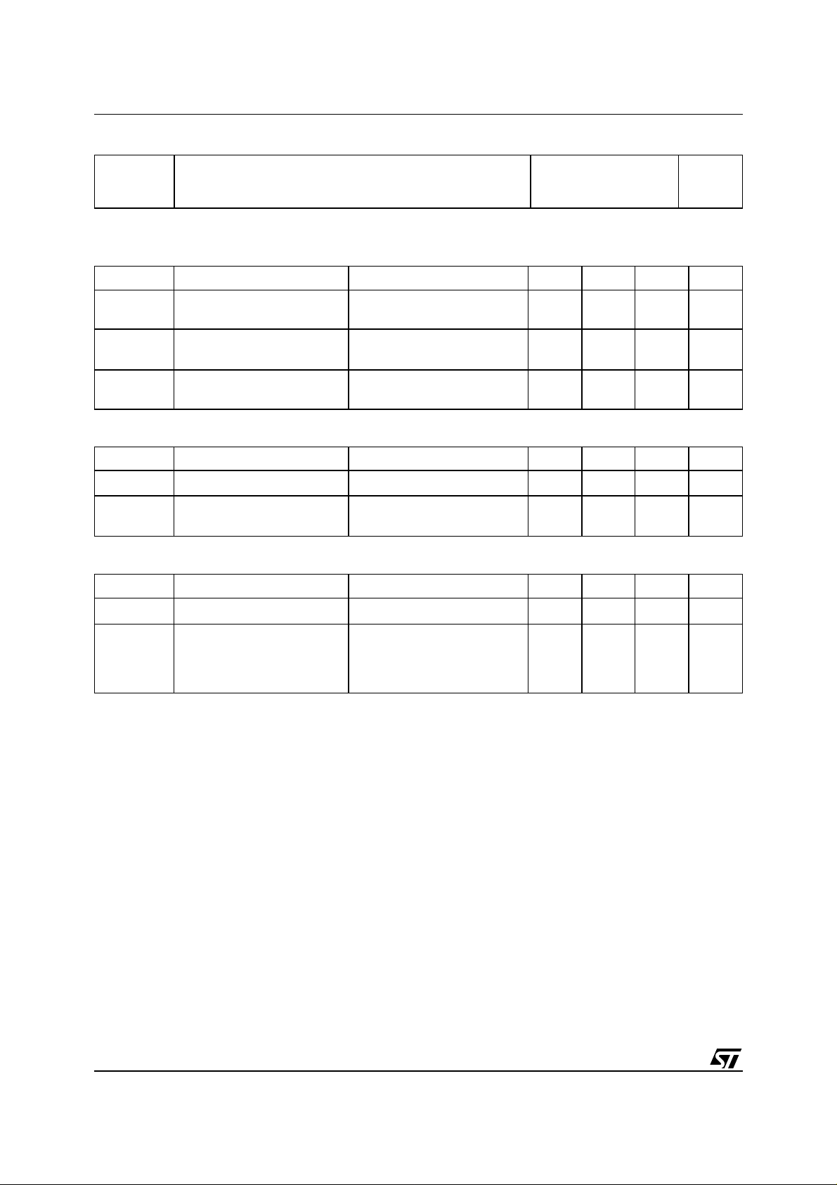
Safe Operating Area
Source-drain Current
(•)
Source-drain Current (pulsed)
(*)
Forward On Voltage
Reverse Recovery Time
Reverse Recovery Charge
Reverse Recovery Current
I
= 100 A VGS = 0
SD
= 100 A di/dt = 100A/µs
I
SD
= 20 V Tj = 150°C
V
DD
(see test circuit, Figure 5)
Thermal Impedance
100
400
1.3 V
75
150
4
A
A
ns
nC
A
3/11
STB100NF03L-03 STP100NF03L-03 STB100NF03L-03-1
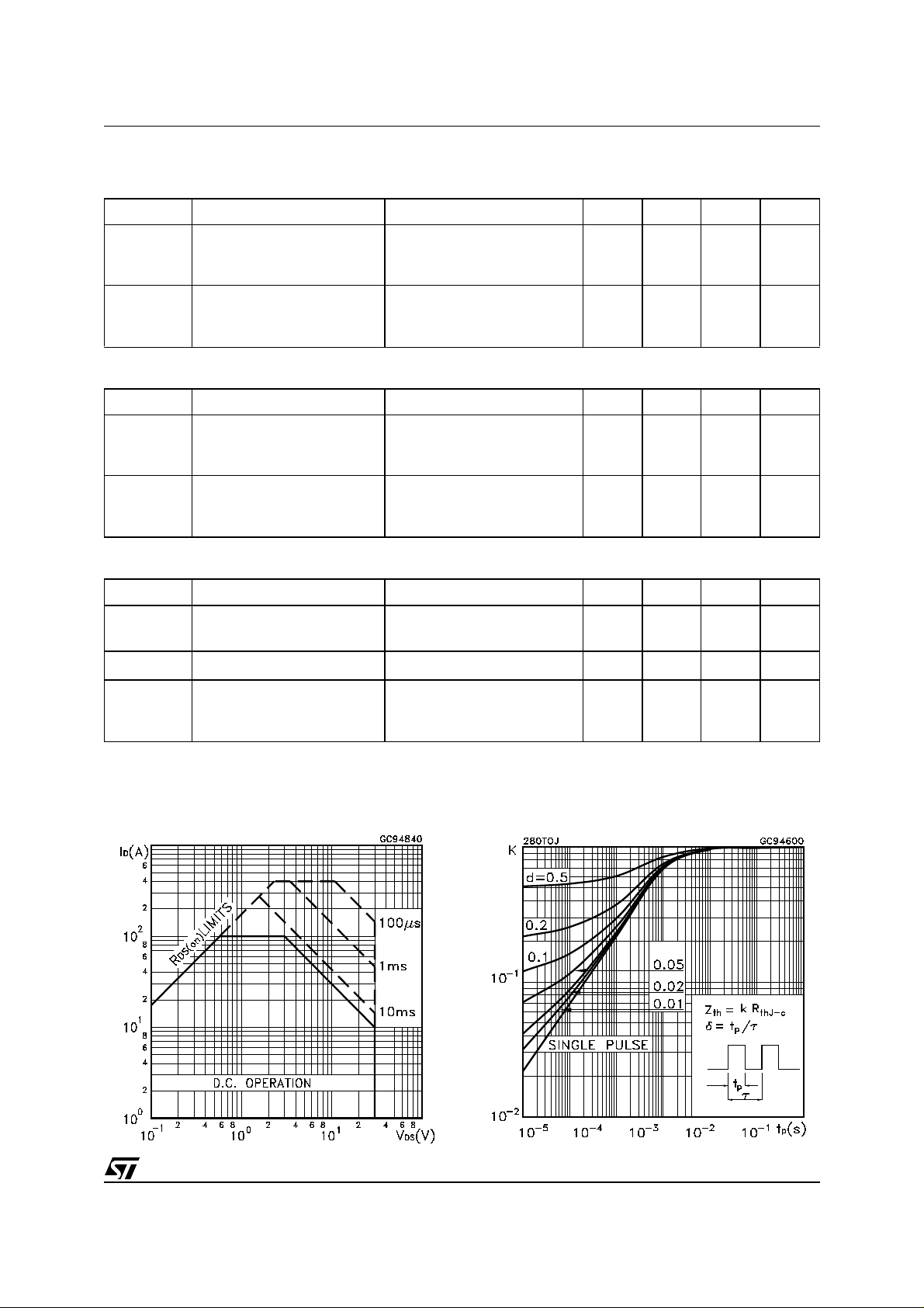
Output Characteristics Transfer Characteristics
Transconductance Static Drain-source On Resistance
Gate Charge vs Gate-source Voltage Capacitance Variations
4/11

STB100NF03L-03 STP100NF03L-03 STB100NF03L-03-1
Normalized Gate Threshold Voltage vs Temperature Normalized on Resistance vs Temperature
Source-drain Diode Forward Characteristics Normalized Breakdown Voltage Temperature
. .
5/11

STB100NF03L-03 STP100NF03L-03 STB100NF03L-03-1
Fig. 1: Unclamped Inductive Load Test CircuitFig. 1: Unclamped Inductive Load Test Circuit Fig. 2: Unclam ped I nduct ive Waveform
Fig. 3: Switching Times Test Circuits For Resistive
Load
Fig. 5: Test Circuit For Inductive Load Switching
And Diode Recovery Times
Fig. 4: Gate Charge test Circuit
6/11

STB100NF03L-03 STP100NF03L-03 STB100NF03L-03-1
D2PAK MECHANICAL DATA
DIM.
A 4.4 4.6 0.173 0.181
A1 2.49 2.69 0.098
A2 0.03 0.23 0.001 0.009
B 0.7 0.93 0.028 0.037
B2 1.14 1.7 0.045 0.067
C 0.45 0.6 0.018 0.024
C2 1.21 1.36 0.048 0.054
D 8.95 9.35 0.352 0.368
D1 8 0.315
E 10 10.4 0.394 0.409
E1 8.5 0.334
G 4.88 5.28 0.192 0.208
L 15 15.85 0.591 0.624
L2 1.27 1.4 0.050 0.055
L3 1.4 1.75 0.055 0.069
M 2.4 3.2 0.094 0.126
R 0.4 0.015
V2 0° 8° 0° 8°
MIN. TYP. MAX. MIN. TYP. TYP.
mm. inch.
0.106
7/11

STB100NF03L-03 STP100NF03L-03 STB100NF03L-03-1
TO-262 (I2PAK) MECHANICAL DATA
DIM.
MIN. TYP. MAX. MIN. TYP. MAX.
A 4.4 4.6 0.173 0.181
A1 2.49 2.69 0.098 0.106
B 0.7 0.93 0.027 0.036
B2 1.14 1.7 0.044 0.067
C 0.45 0.6 0.017 0.023
C2 1.23 1.36 0.048 0.053
D 8.95 9.35 0.352 0.368
e 2.4 2.7 0.094 0.106
E 10 10.4 0.393 0.409
L 13.1 13.6 0.515 0.531
L1 3.48 3.78 0.137 0.149
L2 1.27 1.4 0.050 0.055
mm inch
C
A
A1
C2
B2
B
e
E
L1
L2
D
L
P011P5/E
8/11

STB100NF03L-03 STP100NF03L-03 STB100NF03L-03-1
TO-220 MECHANICAL DATA
DIM.
A 4.4 4.6 0.173 0.181
C 1.23 1.32 0.048 0.051
D 2.40 2.72 0.094 0.107
E 0.49 0.70 0.019 0.027
F 0.61 0.88 0.024 0.034
F1 1.14 1.70 0.044 0.067
F2 1.14 1.70 0.044 0.067
G 4.95 5.15 0.194 0.203
G1 2.40 2.70 0.094 0.106
H2 10 10.40 0.393 0.409
L2 16.40 0.645
L3 28.90 1.137
L4 13 14 0.511 0.551
L5 2.65 2.95 0.104 0.116
L6 15.25 15.75 0.600 0.620
L7 6.20 6.60 0.244 0.260
L9 3.50 3.93 0.137 0.154
DIA 3.75 3.85 0.147 0.151
MIN. TYP. MAX. MIN. TYP. TYP.
mm. inch.
9/11

STB100NF03L-03 STP100NF03L-03 STB100NF03L-03-1
D2PAK FOOTPRINT
TAPE AND REEL SHIPMENT (suffix ”T4”)*
TUBE SHIPMENT (no suffix)*
REEL MECHANICAL DATA
DIM.
A 330 12.992
B 1.5 0.059
C 12.8 13.2 0.504 0.520
D 20.2 0.795
G 24.4 26.4 0.960 1.039
N 100 3.937
T 30.4 1.197
mm inch
MIN. MAX. MIN. MAX.
TAPE MECHANICAL DATA
DIM.
A0 10.5 10.7 0.413 0.421
B0 15.7 15.9 0.618 0.626
D 1.5 1.6 0.059 0.063
D1 1.59 1.61 0.062 0.063
E 1.65 1.85 0.065 0.073
F 11.4 11.6 0.449 0.456
K0 4.8 5.0 0.189 0.197
P0 3.9 4.1 0.153 0.161
P1 11.9 12.1 0.468 0.476
P2 1.9 2.1 0075 0.082
R50 1.574
T0.25 0.35 .0.0098 0.0137
W 23.7 24.3 0.933 0.956
mm inch
MIN. MAX. MIN. MAX.
* on sales type
10/11
BASE QTY BULK QTY
1000 1000

STB100NF03L-03 STP100NF03L-03 STB100NF03L-03-1
Information furnishe d is bel i eved to be accurate and reliable. However, STMicroelectroni cs assumes no responsibility for t he consequences
of use of such information nor for any infringement of patents or other rights of third parties which may result from its use. No license is granted
by implic ation or oth erwise unde r any patent or patent rights of STMi croelectronics. Speci fications me ntioned in th i s publication are subject
to change without notice. This publication supersedes and replaces all information previously supplied. STMicroelectronics products are not
authorized for use as crit i cal component s i n l i f e support devices or systems wi thout expre ss written appr oval of STMicroelectronics.
The ST log o i s registered trademark of STM i croelectronics
2002 STMi croelectroni cs - All Right s Reserved
All other names are the property of their respectiv e owners.
Australi a - Brazil - Can ada - China - Finland - France - Germany - Hong Kong - India - Israel - Italy - Japan - Malaysi a - M al ta - Morocco -
Singapor e - S pai n - Sweden - Swit zerland - United Kingdom - U ni t ed States.
STMicroelect ro n ics GRO UP OF COMPANI ES
http://www.st.com
11/11
 Loading...