


high performance GPS multichip module (MCM)
Features
■ GPS multichip module:
– STA2058 TESEO Baseband
– STA5620 RF Front-end
■ Complete embedded memory system:
– Flash 256 KB + 16 Kbytes
– RAM 64 Kbytes.
■ 66-MHz ARM7TDMI 32 bit processor
■ High performance GPS engine (HPGPS)
■ SBAS (WAAS and EGNOS) supported
■ Sensitivity (-146 dBm acquisition, -159 dBm
tracking)
■ Time to first fix (1 s reacquisition, 2.5 s hot start,
34 s warm start, 39 s cold start)
■ Accuracy (2 m autonomous)
■ Extensive GPS receiver interfaces: 32 GPIOs,
4 UARTs, 2 SPIs, 2 I2Cs, 1CANs 2.0,
1 USB 1.1, 1 HDLC and 4 channels ADC
■ Compatible with L1 signal (C/A code)
■ ST proprietary technology
– CMOS Flash embebbed technology for
STA2058
– BiCMOS Sige technology for STA5620
■ LFBGA104 lead-free package
■ -40 °C to 85 °C operating temperature range
Table 1. Device summary
STA8058
TESEO™
Data Brief
LFBGA104 (7x11x1.4 mm)
Evaluation kits
■ STA8058 module reference designs
(17x19 mm and 25x25 mm)
■ Evaluation board hosting STA8058 module
Description
STA8058 TESEO MCM is a fully embedded GPS
engine integrating STA2058 TESEO baseband.
and STA5620 RF front-end. The embedded Flash
memory enables the equipment manufacturer to
load the entire GPS software (including tracking,
acquisition, navigation and data output) after
customising its interfaces to his needs.
A standard GPS library is available from ST. By
combining the ARM7TDMI microcontroller core
with on-chip Flash/RAM, 16-channel GPS
correlator DSP, RF Front-end and an extensive
range of interfaces on single package solution,
the STA8058 provides a highly-flexible and costeffective solution for GPS applications.
Order Code Package Packing Automotive Grade
STA8058 LFBGA104 (7x11x1.4mm) Tray No
STA8058TR LFBGA104 (7x11x1.4mm) Tape and reel No
STA8058A LFBGA104 (7x11x1.4mm) Tray Yes
STA8058ATR LFBGA104 (7x11x1.4mm) Tape and reel Yes
March 2009 Rev 2 1/14
For further information contact your local STMicroelectronics sales office.
www.st.com
14

Contents STA8058
Contents
1 Features summary . . . . . . . . . . . . . . . . . . . . . . . . . . . . . . . . . . . . . . . . . . 3
2 Pin description . . . . . . . . . . . . . . . . . . . . . . . . . . . . . . . . . . . . . . . . . . . . . 5
2.1 Logic symbol . . . . . . . . . . . . . . . . . . . . . . . . . . . . . . . . . . . . . . . . . . . . . . . 5
2.2 System block diagram . . . . . . . . . . . . . . . . . . . . . . . . . . . . . . . . . . . . . . . . 6
2.3 LFBGA104 ball out . . . . . . . . . . . . . . . . . . . . . . . . . . . . . . . . . . . . . . . . . . . 9
2.4 Power supply pins . . . . . . . . . . . . . . . . . . . . . . . . . . . . . . . . . . . . . . . . . . . 9
3 Electrical characteristics . . . . . . . . . . . . . . . . . . . . . . . . . . . . . . . . . . . . 11
4 Package information . . . . . . . . . . . . . . . . . . . . . . . . . . . . . . . . . . . . . . . . 12
5 Revision history . . . . . . . . . . . . . . . . . . . . . . . . . . . . . . . . . . . . . . . . . . . 13
2/14

STA8058 Features summary
1 Features summary
● ARM7TDMI 16/32 bit RISC CPU based host microcontroller running at a frequency up
to 66 MHz.
● Complete Embedded Memory System:
– Flash 256 Kbytes + 16 Kbytes (100 KB erasing/programming cycles)
– RAM 64 Kbytes.
● 16 channel High performance GPS correlation DSP.
● ST propietary technology:
– CMOS Flash embedded technology for baseband
– BiCMOS Sige for radio front-end
● SBAS (WAAS and EGNOS) supported.
● -40 °C to 85 °C operating temperature range.
● 104-pin LFBGA104 package.
● Power supply:
– 3.0 V to 3.6 V operating supply range for input/output periphery
– 3.0 V to 3.6 V operating supply range for A/D converter reference
– 1.8 V operating supply range for core supply provided by internal voltage regulator
with external stabilization capacitor or by external supply voltage
– 2.4 V to 3 V operating supply range for RF front-end section
● Reset and clock control unit able to provide low power modes (WAIT, SLOW, STOP,
Standby) and to generate the internal clock from the external reference through
integrated PLL.
● 32 programmable general purpose I/O, each pin programmable independently as
digital input or digital output; 30 are multiplexed with peripheral functions; 16 can
generate an interrupt on input level/transition.
● Real time clock module with 32 kHz low power oscillator and separate power supply to
continue running during stand-by mode.
● 16-bit Watchdog timer with 8 bits prescaler for system reliability and integrity.
● One CAN module compliant with the CAN specification V2.0 part B (active) and bit rate
can be programmed up to 1 MBaud.
● Four 16-bit programmable timers with 7 bit prescaler, up to two input capture/output
compare, one pulse counter function, one PWM channel with selectable frequency
each.
● 4 channels 12-bit sigma-delta analog to digital converter, single channel or multi
channel conversion modes, single-shot or continuous conversion modes, sample rate
1 kHz, conversion range 0-2.5V .
● Three serial communication interfaces (UART) allow full duplex, asynchronous,
communications with external devices, independently programmable TX and RX baud
rates up to 625K baud.
● One UART adapted to suit smart card interface needs, for asynchronous SC as defined
by ISO 7816-3. It includes SC clock generation.
● Two serial peripheral interfaces (SPI) allow full duplex, synchronous communications
with external devices, master or slave operation, max baud rate of 5.5Mb/s. One SPI
may be used as multimedia card interface.
3/14

Features summary STA8058
● Two I
● Enhanced interrupt controller supports 32 interrupt vectors, independently maskable,
2
C interfaces provide multi-master and slave functions, support normal and fast
2
I
C mode (400 KHz), 7/10 bit addressing modes. One I2C Interface is multiplexed with
one SPI, so either 2 x SPI + 1 x I
2
C or 1 x SPI + 2 x I2C may be used at a time.
with interrupt vector table for faster response and 16 priority levels, software
programmable for each source. Up to 2 maskable interrupts may be mapped on FIQ.
● Wake-up unit allows exiting from powerdown modes by detection of an event on two
external pins (one is active high and other is active low) or on internal Real Time Clock
alarm.
● USB unit V1.1 compliant, software configurable endpoint setting, USB suspend/resume
support
● High level data link controller (HDLC) unit supports full duplex operating mode, NRZ,
NRZI, FM0 and MANCHESTER modes, and internal 8-bit Baud Rate Generator.
● RF front-end features:
– LOW IF (4 MHz) architecture
– Compatible with GPS L1 signal
– VGA gain internally regulated
– On chip programmable PLL
– SPI interface
4/14
STA8058 Pin description
2 Pin description
2.1 Logic symbol
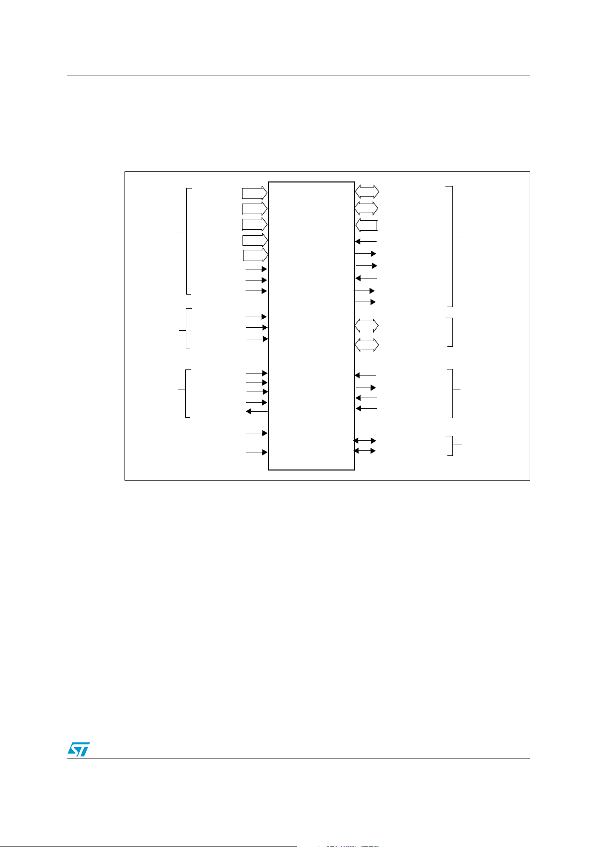
Figure 1. STA8058 TESEO MCM symbol
Power
Pads
Clock
& Reset
JTAG
Por t
V18 [2]
V33 [7]
V27 [8]
VSS [10]
VSSRF [11]
AVSS
AVD D
V18BKP
GPSCLK
CK
RSTINn
JTDI
JTCK
JTMS
JTRSTn
JTDO
BOOTEN
GPSDAT
TESEO
MCM
Xtal (IN,Out,Clk)
SPI (DI,DO,CS, CLK)
Enable (Chip,RF)
Mode
GPS_CLK
Sign
RF_IN
AGC_CNTR
IF_TEST
P0.[15:0]
P1.[15:0]
nSTDBY_I
RTCXTO
RTCXTI
WAKEUP
USBDP
USBDN
RF Pads
GeneraI
Purpose I/O
RTC
& WKUP
Pads
USB Pads
5/14
 Loading...