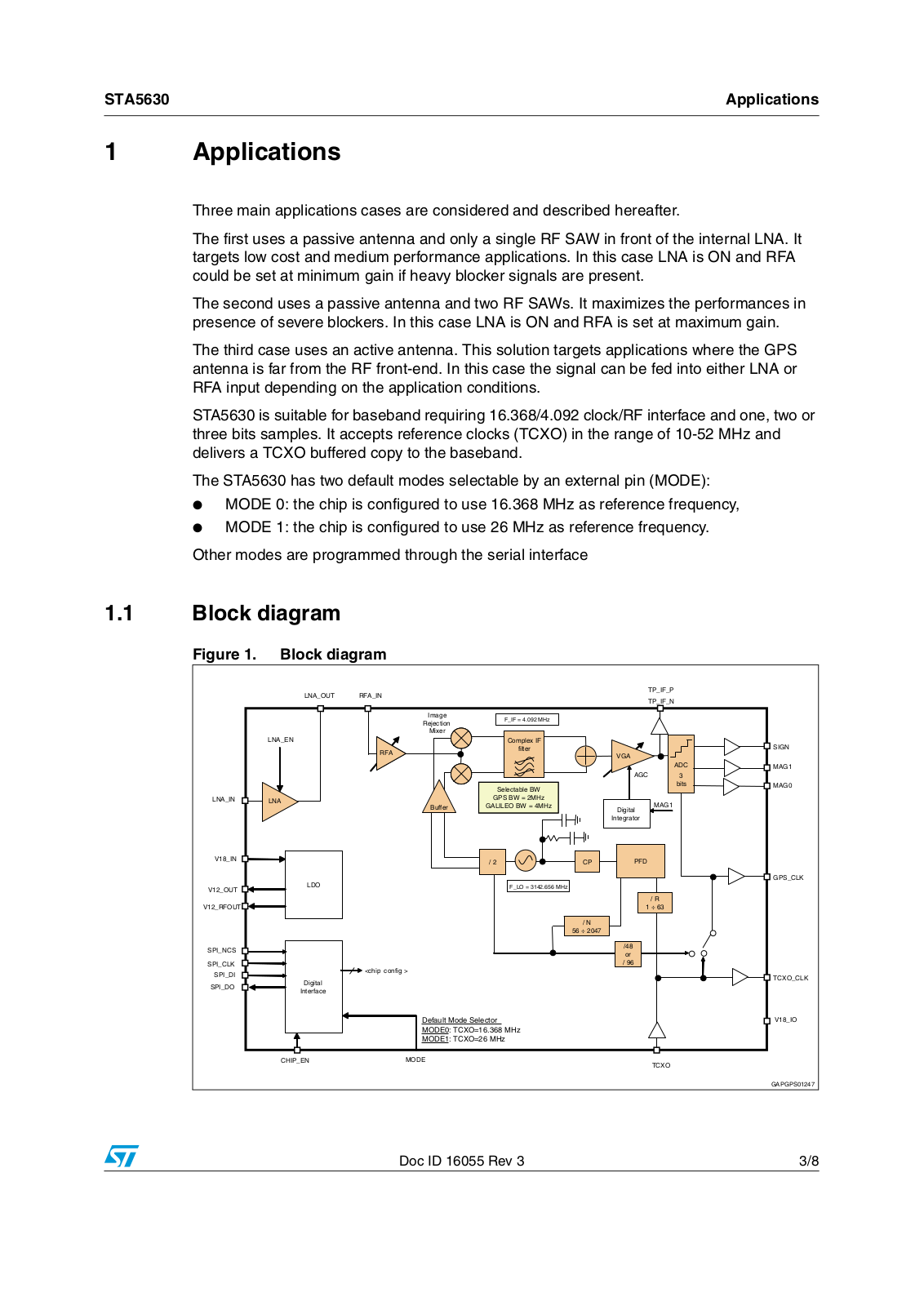
ST STA5630 User Manual

STA5630

Low power GPS RF front-end

Features

Integrated LNA

Low power consumption (< 25 mW)

1.8 V supply voltage

GPS and Galileo compliant

Minimum external components

Serial interface

3 bits A/D converter

CMOS 65 nm technology

Standard QFN-32 package

Ambient temperature range: -40 °C to +85 °C

Description

The STA5630 is a fully integrated RF front-end able to down-convert either the GPS L1 signal from 1575.42 MHz to 4.092 MHz.

The STA5630 embeds high performance LNA minimizing external component count. The chip uses state of the art CMOS 65 nm technology.

A 3-bit ADC converts the IF signal to Sign (SIGN) and Magnitude (MAG0 and MAG1). The magnitude bits are internally integrated in order to control the variable gain amplifiers. The VGA gain can be also set by the SPI interface.

Data brief production data

'!0'03

VFQFPN32

The STA5630 accepts a range of reference clocks (10 to 52 MHz) and generates a 16.368 MHz sampling clock (GPS_CLK) for the baseband. The STA5630 embeds LDO to supply the internal core of the device facilitating requirements to external power supply.

High performance, low power, and cost effective device, the STA5630 is the ideal solution for automotive, cellular and consumer battery powered applications.

Table 1.

Device summary


Order code


Marking

Package

Packing


STA5630TR


STA5630

VFQFPN32

Tape and reel


STA5630ATR (1)


STA5630A

VFQFPN32

Tape and reel

1. Automotive Grade.

June 2012

Doc ID 16055 Rev 3

1/8

This is information on a product in full production. For further information contact your local STMicroelectronics sales

www.st.com

office.


Contents

STA5630


Contents

1

Applications . . . . . . . . . . . . . . . . . . . . . . . . . . . . . . . . . . . . . . . . . . . . . . . .

3


1.1

Block diagram . . . . . . . . . . . . . . . . . . . . . . . . . . . . . . . . . . . . . . . . . . . . . . .

3

2

Pin description . . . . . . . . . . . . . . . . . . . . . . . . . . . . . . . . . . . . . . . . . . . . .

4

3

Package information . . . . . . . . . . . . . . . . . . . . . . . . . . . . . . . . . . . . . . . . .

6

4

Revision history . . . . . . . . . . . . . . . . . . . . . . . . . . . . . . . . . . . . . . . . . . . .

7

2/8

Doc ID 16055 Rev 3

ST STA5630 User Manual

STA5630

Applications


1 Applications

Three main applications cases are considered and described hereafter.

The first uses a passive antenna and only a single RF SAW in front of the internal LNA. It targets low cost and medium performance applications. In this case LNA is ON and RFA could be set at minimum gain if heavy blocker signals are present.

The second uses a passive antenna and two RF SAWs. It maximizes the performances in presence of severe blockers. In this case LNA is ON and RFA is set at maximum gain.

The third case uses an active antenna. This solution targets applications where the GPS antenna is far from the RF front-end. In this case the signal can be fed into either LNA or RFA input depending on the application conditions.

STA5630 is suitable for baseband requiring 16.368/4.092 clock/RF interface and one, two or three bits samples. It accepts reference clocks (TCXO) in the range of 10-52 MHz and delivers a TCXO buffered copy to the baseband.

The STA5630 has two default modes selectable by an external pin (MODE):

MODE 0: the chip is configured to use 16.368 MHz as reference frequency,

MODE 1: the chip is configured to use 26 MHz as reference frequency.

Other modes are programmed through the serial interface

1.1Block diagram

Figure 1. Block diagram


,.!?/54

2&!?).


40?)&?0


40?)&?.


)MAGEE

&?)& -(Z


2EJECTION


-IXER


,.!?%.


#OMPLEXE)&


3)'.


2&!

FILTER


6'!


!$#

-!'


!'#


3ELECTABLEE"7


BITS

-!'


,.!?).

,.!


'03 "7 -(Z


-!'


"UFFER

'!,),%/ "7 -(Z


$IGITAL


)NTEGRATOR


6 ?).


#0

0&$


,$/


'03?#,+

6 ?/54


&?,/ -(Z


2


6 ?2&/54


.


30)?.#3


OR


30)?#,+


CHIPP CONFIG


30)?$)


4#8/?#,+


$IGITAL


30)?$/


)NTERFACE


$EFAULTT-ODE 3ELECTOR


6 ?)/


-/$% 4#8/ -(Z


-/$% 4#8/ -(Z


#()0?%.

-/$%


4#8/


'!0'03

Doc ID 16055 Rev 3

3/8

Loading...
+ 5 hidden pages