

Features
■ High output power capability
– 2x 38 W into 4 Ω at 18 V, 1 kHz, 10% THD
– 2x 34 W into 8 Ω at 22 V, 1 kHz, 10% THD
– 2x 24W into 4Ω at 14.4 V, 1 kHz, 10% THD
– 2x 15 W into 8 Ω at 16 V, 1 kHz, 10% THD
– 4x 13 W into 2 Ω at 15 V, 1 kHz, 10% THD
– 4x 11 W into 4 Ω at 18 V, 1 kHz, 10% THD
– 4x 7 W into 4 Ω at 14.4 V, 1 kHz, 10% THD
■ Minimum external components count:
– no bootstrap capacitors
– no Boucherot cells
– internally fixed gain 20 dB
■ Standby function (CMOS compatible)
■ No audible pop during standby operations
■ Diagnostic facilities:
– clip detector
– output to GND short-circuit detector
– output to VS short-circuit detector
– soft short-circuit check at turn-on
– thermal shutdown warning
STA540
4 x 13 W dual/quad power amplifier
Datasheet − production data
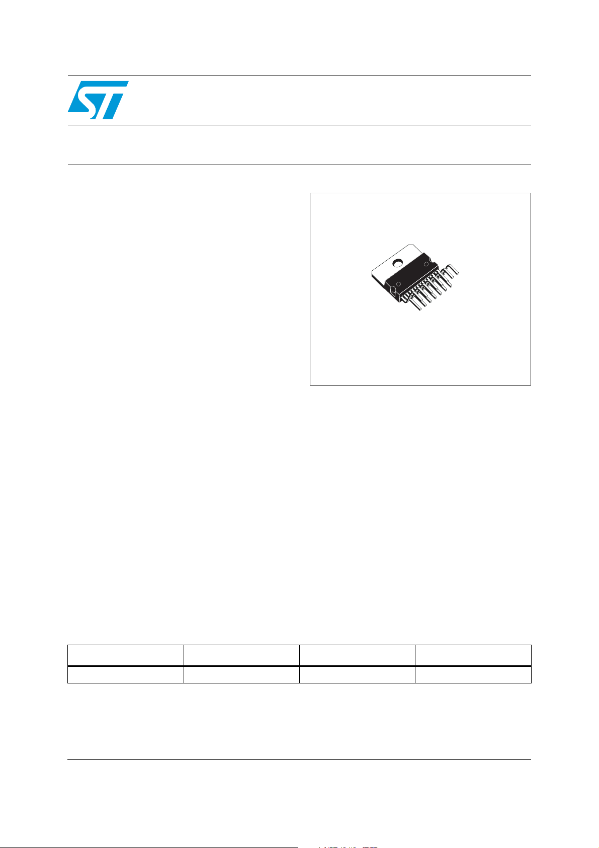
Multiwatt15
Description
The STA540 is a 4-channel, class-AB audio
amplifier designed for high quality sound
applications.
The amplifiers have single-ended outputs with
integrated short-circuit protection, thermal
protection and diagnostic functions.
Protection
■ Output AC/DC short circuit
■ Soft short-circuit check at turn-on
■ Thermal cutoff/limiter to prevent chip from
The chip is housed in the 15-pin Multiwatt
ECOPACK
®
Pb-free package which is RoHS
(2002/95/EC) compliant.
overheating
■ High inductive loads
■ ESD
Table 1. Device summary
Order code Temperature range Package Packing
STA540 -40 to 150° C Multiwatt15 Tube
April 2012 Doc ID 13907 Rev 6 1/25
This is information on a product in full production.
www.st.com
1

Contents STA540
Contents
1 Block diagram and pin description . . . . . . . . . . . . . . . . . . . . . . . . . . . . . 6
1.1 Block diagram . . . . . . . . . . . . . . . . . . . . . . . . . . . . . . . . . . . . . . . . . . . . . . . 6
1.2 Pin description . . . . . . . . . . . . . . . . . . . . . . . . . . . . . . . . . . . . . . . . . . . . . . 7
2 Electrical specifications . . . . . . . . . . . . . . . . . . . . . . . . . . . . . . . . . . . . . . 8
2.1 Absolute maximum ratings . . . . . . . . . . . . . . . . . . . . . . . . . . . . . . . . . . . . . 8
2.2 Thermal data . . . . . . . . . . . . . . . . . . . . . . . . . . . . . . . . . . . . . . . . . . . . . . . 8
2.3 Electrical characteristics . . . . . . . . . . . . . . . . . . . . . . . . . . . . . . . . . . . . . . . 8
3 Standard application circuits . . . . . . . . . . . . . . . . . . . . . . . . . . . . . . . . . 10
4 Electrical characteristics curves . . . . . . . . . . . . . . . . . . . . . . . . . . . . . . 12
5 Thermal information . . . . . . . . . . . . . . . . . . . . . . . . . . . . . . . . . . . . . . . . 15
5.1 Heatsink specification examples . . . . . . . . . . . . . . . . . . . . . . . . . . . . . . . 15
5.1.1 R
5.1.2 R
5.1.3 Calculations using music power . . . . . . . . . . . . . . . . . . . . . . . . . . . . . . . 16
calculation for 4 single-ended channels . . . . . . . . . . . . . . . . . . . 15
th_HS
calculation for 2 single-ended channels plus 1 BTL channel . . . 15
th_HS
6 Practical information . . . . . . . . . . . . . . . . . . . . . . . . . . . . . . . . . . . . . . . . 17
6.1 Highly flexible amplifier configuration . . . . . . . . . . . . . . . . . . . . . . . . . . . . 17
6.2 Easy single-ended to bridge transition . . . . . . . . . . . . . . . . . . . . . . . . . . . 17
6.3 Internally fixed gain . . . . . . . . . . . . . . . . . . . . . . . . . . . . . . . . . . . . . . . . . 17
6.4 Silent turn on/off and muting/standby function . . . . . . . . . . . . . . . . . . . . . 17
6.5 Driving circuit for standby mode . . . . . . . . . . . . . . . . . . . . . . . . . . . . . . . . 17
6.6 Output stage . . . . . . . . . . . . . . . . . . . . . . . . . . . . . . . . . . . . . . . . . . . . . . . 18
6.6.1 Rail-to-rail output voltage swing without bootstrap capacitors . . . . . . . . 18
6.6.2 Absolute stability without external compensation . . . . . . . . . . . . . . . . . 18
6.7 Built–in protection . . . . . . . . . . . . . . . . . . . . . . . . . . . . . . . . . . . . . . . . . . . 19
6.7.1 Diagnostic facilities (pin 10) . . . . . . . . . . . . . . . . . . . . . . . . . . . . . . . . . . 19
6.7.2 Short-circuit protection . . . . . . . . . . . . . . . . . . . . . . . . . . . . . . . . . . . . . . 19
6.7.3 Clipping detection . . . . . . . . . . . . . . . . . . . . . . . . . . . . . . . . . . . . . . . . . 20
6.7.4 Thermal shutdown . . . . . . . . . . . . . . . . . . . . . . . . . . . . . . . . . . . . . . . . . 20
2/25 Doc ID 13907 Rev 6

STA540 Contents
6.8 Handling the diagnostic information . . . . . . . . . . . . . . . . . . . . . . . . . . . . . 21
6.9 PCB ground layout . . . . . . . . . . . . . . . . . . . . . . . . . . . . . . . . . . . . . . . . . . 22
6.10 Mute function . . . . . . . . . . . . . . . . . . . . . . . . . . . . . . . . . . . . . . . . . . . . . . 22
7 Package information . . . . . . . . . . . . . . . . . . . . . . . . . . . . . . . . . . . . . . . . 23
8 Revision history . . . . . . . . . . . . . . . . . . . . . . . . . . . . . . . . . . . . . . . . . . . 24
Doc ID 13907 Rev 6 3/25

List of tables STA540
List of tables
Table 1. Device summary . . . . . . . . . . . . . . . . . . . . . . . . . . . . . . . . . . . . . . . . . . . . . . . . . . . . . . . . . . 1
Table 2. Pin description . . . . . . . . . . . . . . . . . . . . . . . . . . . . . . . . . . . . . . . . . . . . . . . . . . . . . . . . . . . 7
Table 3. Absolute maximum ratings . . . . . . . . . . . . . . . . . . . . . . . . . . . . . . . . . . . . . . . . . . . . . . . . . . 8
Table 4. Thermal data. . . . . . . . . . . . . . . . . . . . . . . . . . . . . . . . . . . . . . . . . . . . . . . . . . . . . . . . . . . . . 8
Table 5. Electrical characteristics . . . . . . . . . . . . . . . . . . . . . . . . . . . . . . . . . . . . . . . . . . . . . . . . . . . . 8
Table 6. Document revision history . . . . . . . . . . . . . . . . . . . . . . . . . . . . . . . . . . . . . . . . . . . . . . . . . 24
4/25 Doc ID 13907 Rev 6

STA540 List of figures
List of figures
Figure 1. Block diagram . . . . . . . . . . . . . . . . . . . . . . . . . . . . . . . . . . . . . . . . . . . . . . . . . . . . . . . . . . . . 6
Figure 2. Pin connection (top view) . . . . . . . . . . . . . . . . . . . . . . . . . . . . . . . . . . . . . . . . . . . . . . . . . . . 7
Figure 3. Quadraphonic . . . . . . . . . . . . . . . . . . . . . . . . . . . . . . . . . . . . . . . . . . . . . . . . . . . . . . . . . . 10
Figure 4. Alternative single-ended speaker connection . . . . . . . . . . . . . . . . . . . . . . . . . . . . . . . . . . 10
Figure 5. Dual bridge . . . . . . . . . . . . . . . . . . . . . . . . . . . . . . . . . . . . . . . . . . . . . . . . . . . . . . . . . . . . 10
Figure 6. Stereo plus bridge drive . . . . . . . . . . . . . . . . . . . . . . . . . . . . . . . . . . . . . . . . . . . . . . . . . . . 11
Figure 7. Quiescent drain current versus supply voltage (single-ended and bridge). . . . . . . . . . . . . 12
Figure 8. Quiescent output voltage versus supply voltage (single-ended and bridge). . . . . . . . . . . . 12
Figure 9. Output power versus supply voltage. . . . . . . . . . . . . . . . . . . . . . . . . . . . . . . . . . . . . . . . . . 12
Figure 10. Output power versus supply voltage. . . . . . . . . . . . . . . . . . . . . . . . . . . . . . . . . . . . . . . . . . 12
Figure 11. Output power versus supply voltage. . . . . . . . . . . . . . . . . . . . . . . . . . . . . . . . . . . . . . . . . . 12
Figure 12. Distortion versus output power . . . . . . . . . . . . . . . . . . . . . . . . . . . . . . . . . . . . . . . . . . . . . . 12
Figure 13. Distortion versus output power . . . . . . . . . . . . . . . . . . . . . . . . . . . . . . . . . . . . . . . . . . . . . . 13
Figure 14. Distortion versus output power . . . . . . . . . . . . . . . . . . . . . . . . . . . . . . . . . . . . . . . . . . . . . . 13
Figure 15. Output power versus supply voltage. . . . . . . . . . . . . . . . . . . . . . . . . . . . . . . . . . . . . . . . . . 13
Figure 16. Output power versus supply voltage. . . . . . . . . . . . . . . . . . . . . . . . . . . . . . . . . . . . . . . . . . 13
Figure 17. Supply voltage rejection versus frequency . . . . . . . . . . . . . . . . . . . . . . . . . . . . . . . . . . . . . 13
Figure 18. Crosstalk versus frequency . . . . . . . . . . . . . . . . . . . . . . . . . . . . . . . . . . . . . . . . . . . . . . . . 13
Figure 19. Standby attenuation versus threshold voltage . . . . . . . . . . . . . . . . . . . . . . . . . . . . . . . . . . 14
Figure 20. Total power dissipation and efficiency versus output power . . . . . . . . . . . . . . . . . . . . . . . . 14
Figure 21. Total power dissipation and efficiency versus output power . . . . . . . . . . . . . . . . . . . . . . . . 14
Figure 22. The new output stage . . . . . . . . . . . . . . . . . . . . . . . . . . . . . . . . . . . . . . . . . . . . . . . . . . . . 18
Figure 23. Shared capacitor in single-ended configuration . . . . . . . . . . . . . . . . . . . . . . . . . . . . . . . . . 19
Figure 24. Clipping detection waveforms . . . . . . . . . . . . . . . . . . . . . . . . . . . . . . . . . . . . . . . . . . . . . . 20
Figure 25. Output fault waveforms (see Figure 26) . . . . . . . . . . . . . . . . . . . . . . . . . . . . . . . . . . . . . . . 20
Figure 26. Fault waveforms . . . . . . . . . . . . . . . . . . . . . . . . . . . . . . . . . . . . . . . . . . . . . . . . . . . . . . . . 20
Figure 27. Waveforms . . . . . . . . . . . . . . . . . . . . . . . . . . . . . . . . . . . . . . . . . . . . . . . . . . . . . . . . . . . . . 21
Figure 28. Interface circuit diagram . . . . . . . . . . . . . . . . . . . . . . . . . . . . . . . . . . . . . . . . . . . . . . . . . . . 21
Figure 29. Optional mute function circuit . . . . . . . . . . . . . . . . . . . . . . . . . . . . . . . . . . . . . . . . . . . . . . 22
Figure 30. Mechanical data and package dimensions (Multiwatt15) . . . . . . . . . . . . . . . . . . . . . . . . . 23
Doc ID 13907 Rev 6 5/25

Block diagram and pin description STA540
1 Block diagram and pin description
1.1 Block diagram
Figure 1. Block diagram
VCC1VCC2
V
CC2VCC1
IN1
ST-BY
ST-BY
IN2
IN3
IN4
13
4
7
5
12
11
3
689
SVR P-GND S-GND
A1
+
-
A2 INV
+
-
A3
+
-
A4 INV
+
-
1
2
15
14
10
OUT1
OUT2
OUT3
OUT4
DIAGNOSTIC
DIAGNOSTICD
OUTPUT
D06AU1630
6/25 Doc ID 13907 Rev 6
STA540 Block diagram and pin description
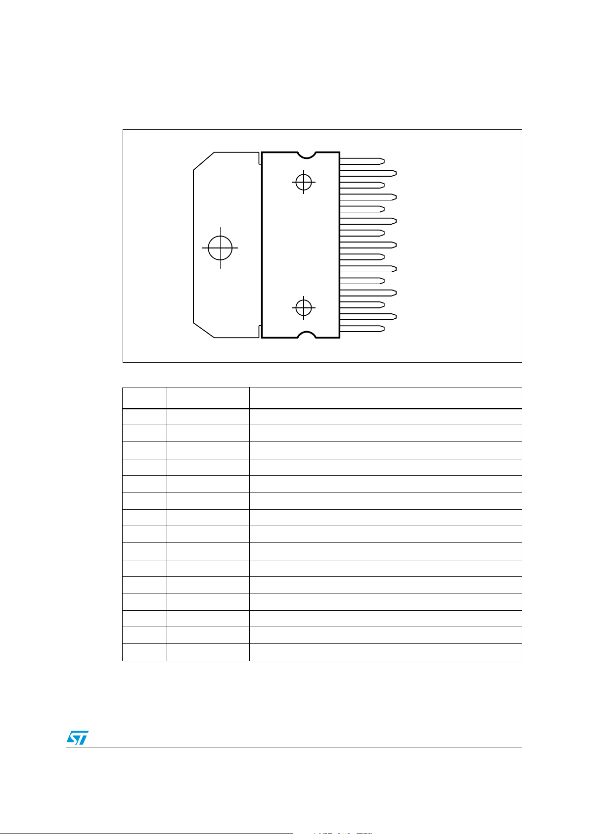
1.2 Pin description
Figure 2. Pin connection (top view)
OUT3
15
14
13
12
11
10
9
8
7
6
5
4
3
2
1
OUT3
OUT4
OUT4
VCC2
VCC
IN3
IN3
IN4
IN4
DIAGNOSTICD
DIAGNOSTICD
S-GND
S-GND
P-GND
PW-GND
ST-BY
STAND-BY
SVR
SVR
IN2
IN2
IN1
IN1
VCC1
VCC
OUT2
OUT2
OUT1
OUT1
D06au1631
Table 2. Pin description
N° Name Type Function
1 OUT1 OUT Channel 1 output
2 OUT2 OUT Channel 2 output
3 VCC1 PWR Power supply
4 IN1 IN Channel 1 input
5 IN2 IN Channel 2 input
6 SVR IN Supply voltage rejection
7 ST-BY IN Standby control pin
8 P-GND PWR Power ground
9 S-GND PWR Signal ground
10 DIAGNOSTICD OUT Diagnostics output
11 IN4 IN Channel 4 input
12 IN3 IN Channel 3 input
13 VCC2 PWR Power supply
14 OUT4 OUT Channel 4 output
15 OUT3 OUT Channel 3 output
Doc ID 13907 Rev 6 7/25
Electrical specifications STA540
2 Electrical specifications
2.1 Absolute maximum ratings
Table 3. Absolute maximum ratings
Symbol Parameter Value Unit
Supply voltage idle mode (no signal) 24 V
V
Supply voltage operating 22 V
s
Supply voltage AC-DC short safe 20 V
P
T
stg
Total power dissipation (T
tot
case
, TjStorage and junction temperature -40 to150 °C
Operating temperature 0 to 70 °C
T
op
2.2 Thermal data
Table 4. Thermal data
Symbol Parameter Value Unit
R
th j-case
R
th j-amb
Thermal resistance junction to case (max) 1.8 °C/W
Thermal resistance junction to ambient (max) 35 °C/W
2.3 Electrical characteristics
The test conditions are VS = 14.4 V, RL = 4 Ω, f = 1 kHz, T
specified.
Table 5. Electrical characteristics
Symbol Parameter Test condition Min Typ Max Unit
V
Supply voltage range 8 22 V
S
Total quiescent drain
I
d
current
V
Output offset voltage -150 150 mV
os
Output power, SE
P
o
Output power, BTL
= 85 °C) 36 W
= 25° C unless otherwise
amb
80 150 mA
THD=10%, R
THD=10%, R
THD=10%, R
THD=10%, R
THD=10%, R
=4 Ω
L
=2 Ω
L
=4 Ω, VS=22 V
L
=4 Ω
L
=8 Ω, VS=17 V
L
THD=10%, RL=8 Ω, VS=22 V
6.5
21
7
11.5
16
24
20
34
W
W
THD Total harmonic distortion R
Short-circuit output current 4.0 A
I
SC
= 4 Ω, Po = 0.1 to 4 W 0.02 %
L
8/25 Doc ID 13907 Rev 6
 Loading...