

18-volt, 3-amp, quad power half-bridge
Features
■ Multipower BCD technology
■ Low input/output pulse width distortion
■ 200-mΩ R
stage
■ CMOS-compatible logic inputs
■ Thermal protection
■ Thermal warning output
■ Undervoltage protection
■ Short-circuit protection
Description
The STA533WF is a monolithic quad half-bridge
stage in multipower BCD technology. The device
can be used as a dual bridge or reconfigured, by
connecting pin CONFIG to pins VDD, as a single
bridge with double-current capability.
The device is designed for the output stage of a
stereo Full Flexible Amplifier (FFX™). It is
capable of delivering 10 W x 4 channels into 4-Ω
Table 1. Device summary
complementary DMOS output
dsON
STA533WF
PowerSSO36 package
with exposed pad down
loads with 10% THD at V
single-ended configuration.
It can also deliver 20 W + 20 W into 8-Ω loads
with 10% THD at V
= 18 V in BTL configuration
CC
or, in single parallel BTL configuration, 40 W into
a 4-Ω load with 10% THD at V
The input pins have a threshold proportional to
the voltage on pin VL.
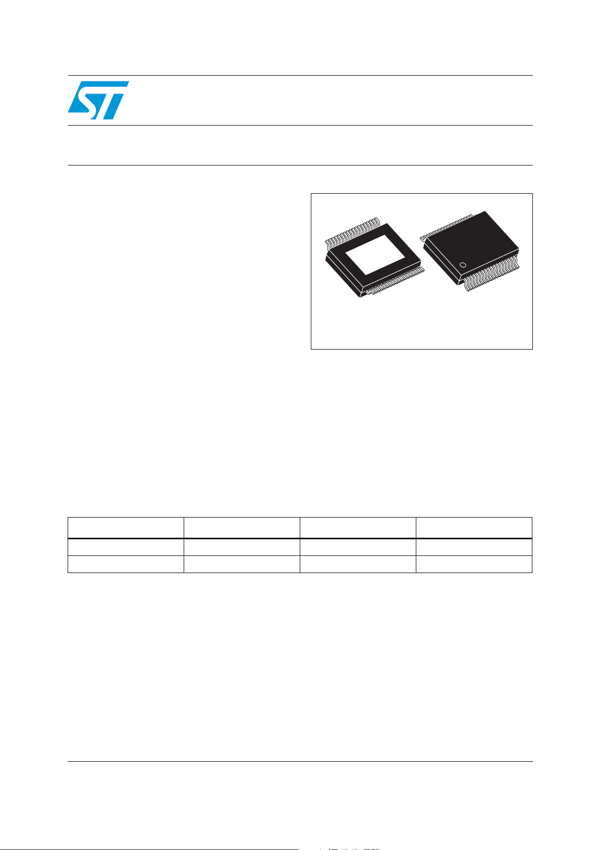
The STA533WF comes in a 36-pin PowerSSO
package with exposed pad down (EPD).
=18V in
CC
= 18 V.
CC
Order code Temperature range Package Packaging
STA533WF 0 to 70 °C PowerSSO36 EPD Tube
STA533WF13TR 0 to 70 °C PowerSSO36 EPD Tape and reel
June 2011 Doc ID 17658 Rev 2 1/15
www.st.com
15
Pin description STA533WF
1 Pin description
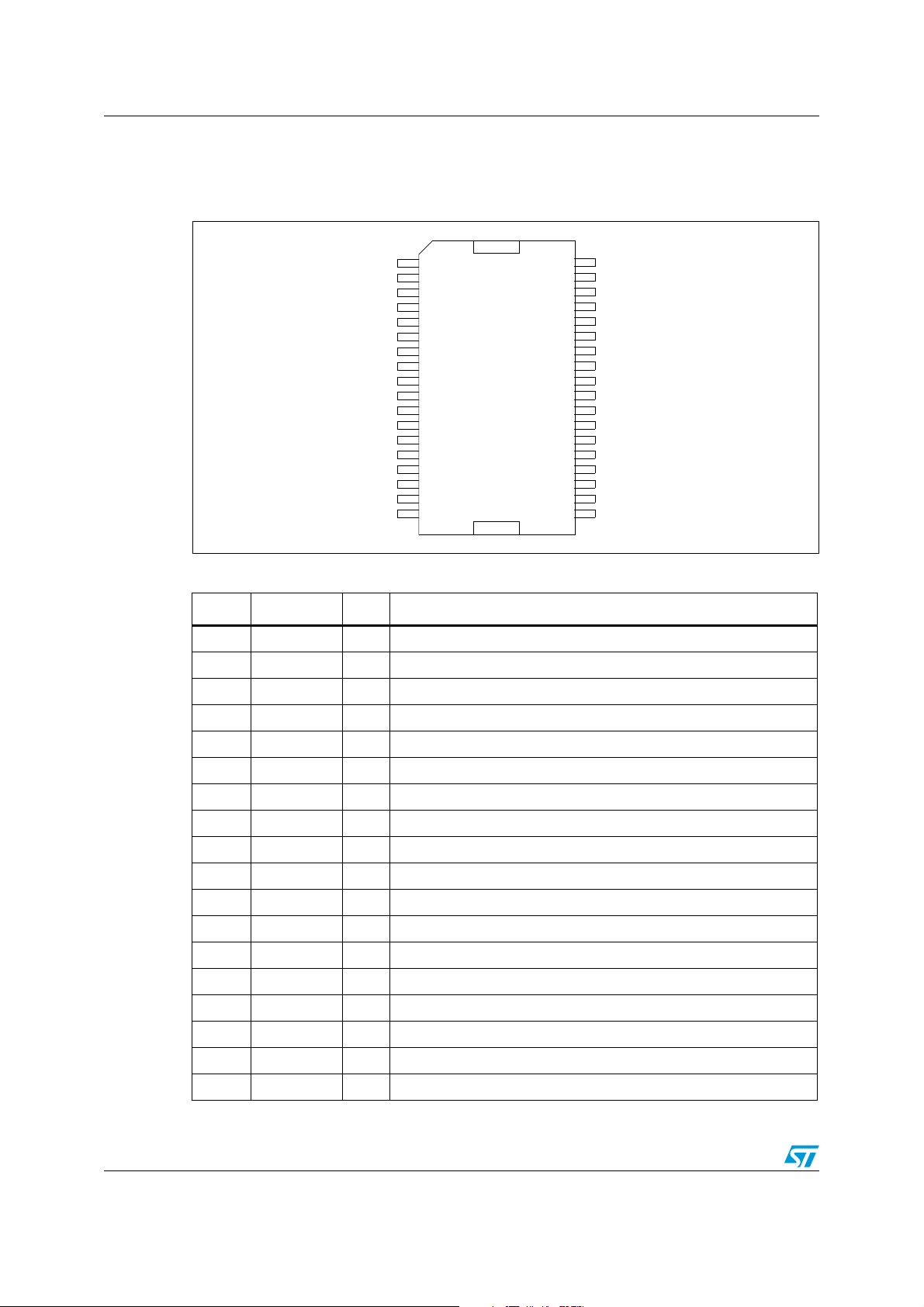
Figure 1. Pin out
Table 2. Pin list
GNDSUB
OUT2B
OUT2B
VCC2B
GND2B
GND2A
VCC2A
OUT2A
OUT2A
OUT1B
OUT1B
VCC1B
GND1B
GND1A
VCC1A
OUT1A
OUT1A
N.C.
1
2
3
4
5
6
7
8
9
10
11
12
13
14
15
16
17
18
STA533WF
36
35
34
33
32
31
30
29
28
27
26
25
24
23
22
21
20
19
Pin Name Type Description
1 GNDSUB PWR Substrate ground
2, 3 OUT2B O Output half-bridge 2B
4 VCC2B PWR Positive supply
VCCSIG
VCCSIG
VSS
VSS
IN2B
IN2A
IN1B
IN1A
THWARN
FAU LT
TRISTATE
PWRDN
CONFIG
VL
VDD
VDD
GNDREG
GNDCLEAN
5 GND2B PWR Negative supply
6 GND2A PWR Negative supply
7 VCC2A PWR Positive supply
8, 9 OUT2A O Output half-bridge 2A
10, 11 OUT1B O Output half-bridge 1B
12 VCC1B PWR Positive supply
13 GND1B PWR Negative supply
14 GND1A PWR Negative supply
15 VCC1A PWR Positive supply
16, 17 OUT1A O Output half-bridge 1A
18 N.C. - No internal connection
19 GNDCLEAN PWR Logical ground
20 GNDREG PWR Filtering for regulator; this is an internally generated ground for V
21, 22 VDD PWR 5-V regulator referred to ground
23 VL PWR High logical state setting voltage, V
2/15 Doc ID 17658 Rev 2
DD
L
STA533WF Pin description
Table 2. Pin list (continued)
Pin Name Type Description
Configuration pin:
24 CONFIG I
25 PWRDN I
26 TRISTATE I
27 FAULT O
28 THWARN O
29 IN1A I Input of half-bridge 1A
30 IN1B I Input of half-bridge 1B
0: normal operation
1: bridges in parallel, see Parallel-output and high-current operation
on page 8
Stand-by pin:
0: low-power mode
1: normal operation
Hi-Z pin:
0: all power amplifier outputs in high-impedance state
1: normal operation
Fault pin advisor (open-drain device, needs pull-up resistor):
0: fault detected (short circuit or thermal, for example)
1: normal operation
Thermal-warning advisor (open-drain device, needs pull-up
resistor):
o
0: temperature of the IC >130
C
1: normal operation
31 IN2A I Input of half-bridge 2A
32 IN2B I Input of half-bridge 2B
33, 34 VSS PWR 5-V regulator referred to +V
CC
35, 36 VCCSIG PWR Filtering for regulator, this is an internally generated supply for V
SS
Doc ID 17658 Rev 2 3/15
Electrical characteristics STA533WF
2 Electrical characteristics
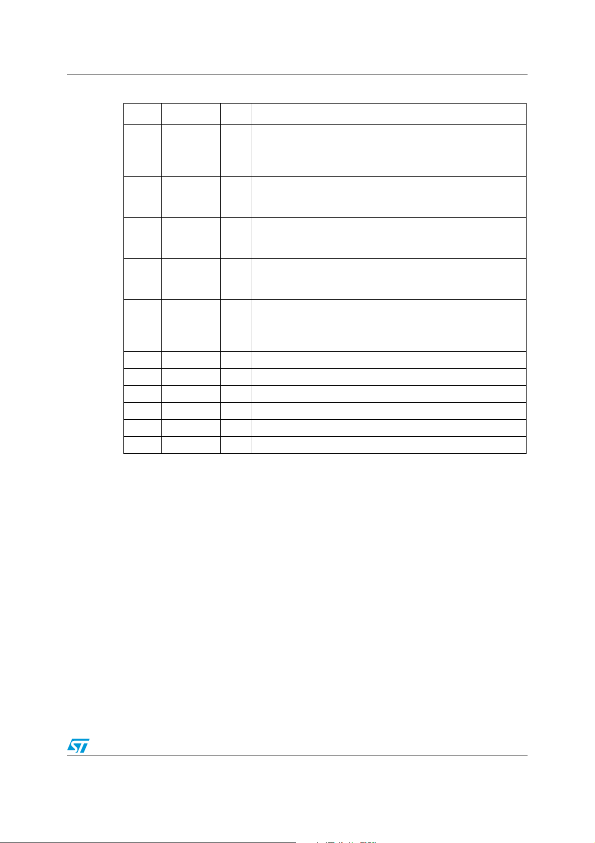
Table 3. Absolute maximum ratings
Symbol Parameter Value Unit
V
CC
V
Lmax
V
inputs
V
config
T
stg
Table 4. Recommended operating conditions
DC supply voltage (Pins 4, 7, 12, 15) 23 V
Voltage on pin 23 4.0 V
Voltage on pins 25, 26, 29 to 32 -0.3 to VL + 0.3 V
Voltage on pins 24 -0.3 to VDD + 0.3 V
, TjStorage and junction temperature -40 to 150 °C
Symbol Parameter Min Typ Max Unit
V
CC
V
L
T
amb
Table 5. Thermal data
DC supply voltage (Pins 4, 7, 12, 15) 5.0 - 18 V
Input logic reference 2.7 3.3 3.6 V
Ambient temperature 0 - 70 °C
Symbol Parameter Min Typ Max Unit
T
j-case
T
jSD
T
warn
t
hSD
Thermal resistance junction to case (thermal pad) - - 1.5 °C/W
Thermal shut-down junction temperature - 150 - °C
Thermal warning temperature - 130 - °C
Thermal shut-down hysteresis - 25 - °C
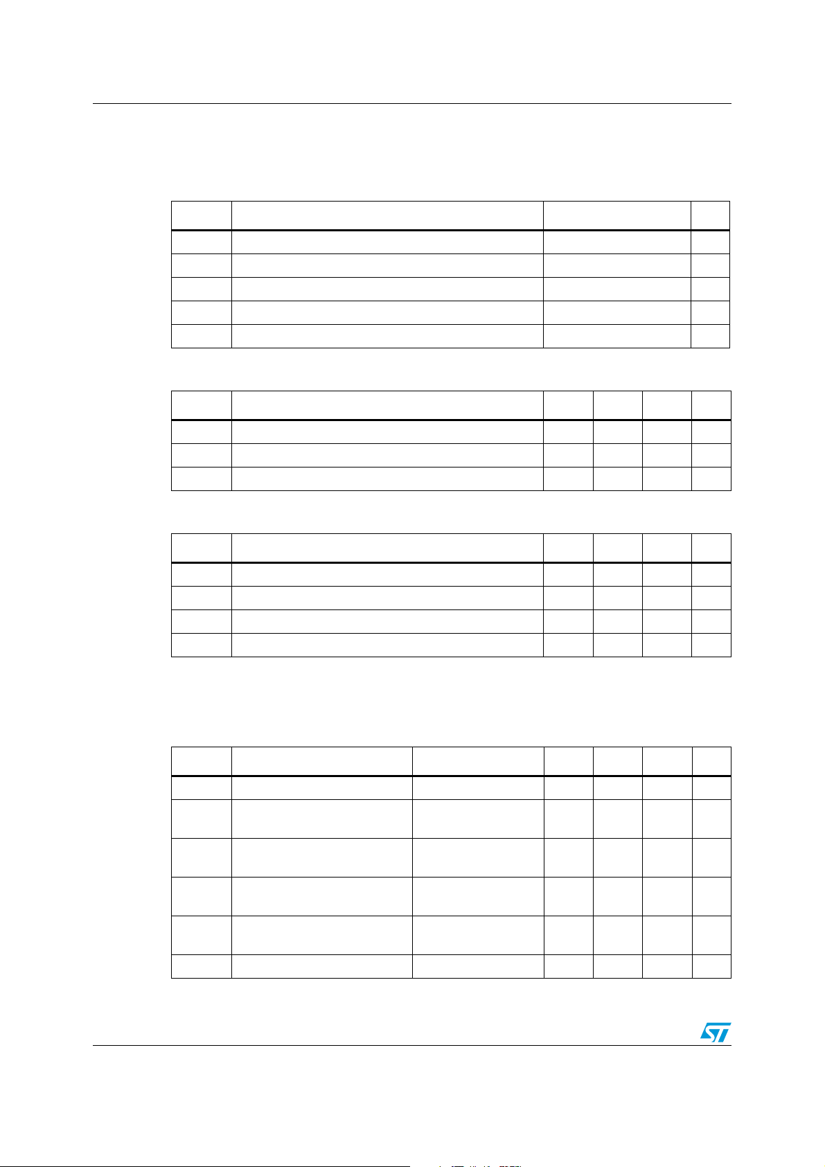
Unless otherwise stated, the test conditions for Ta bl e 6 below are VL = 3.3 V, VCC = 18 V,
R
=8Ω, fSW = 384 kHz and T
L
Table 6. Electrical characteristics
Symbol Parameter Test conditions Min Typ Max Unit
P
R
I
dss
g
N
g
P
OUT
dsON
Output power in BTL mode THD+N > 10% - 20 - W
Power P-channel/N-channel
MOSFET on resistance
Power P-channel/N-channel
leakage
Power P-channel R
matching
Power N-channel R
matching
Dt_s Low current dead time (static) see Figure 2 - 5 10 ns
4/15 Doc ID 17658 Rev 2
amb
dsON
dsON
= 25 °C.
= 1 A - 180 230 mΩ
I
dd
- --10μA
I
= 1 A 95--%
dd
= 1 A 95--%
I
dd
STA533WF Electrical characteristics
Table 6. Electrical characteristics (continued)
Symbol Parameter Test conditions Min Typ Max Unit
Dt_d
t
d_ON
t
d OFF
t
r
t
f
V
IN-Low
V
IN-High
I
IN-H
I
IN-L
I
PWRDN-H
V
Low
V
High
High current dead time
(dynamic)
L = 22 μH, C = 470 nF
= 8 Ω, Idd = 2.0 A
R
L
see Figure 3
- 1020ns
Turn-on delay time Resistive load - 40 60 ns
Turn-off delay time Resistive load - 40 60 ns
Rise time
Fall time
Half-bridge input, low-level
voltage
Half-bridge input, high-level
voltage
High-level input current VIN = V
Resistive load
see Figure 2
Resistive load
see Figure 2
-
-
L
- 8 10 ns
- 8 10 ns
/ 2 -
V
-
VL / 2 +
300 mV
-
-
L
300 mV
-
V
V
-1-μA
Low-level input current VIN = 0.3 V - 1 - μA
High level PWRDN pin input
current
Low logical state voltage
(pins PWRDN, TRISTATE)
High logical state voltage
(pins PWRDN, TRISTATE)
= 3.3 V - 35 - μA
V
L
= 3.3V --0.8V
V
L
V
= 3.3 V 1.7 - - V
L
I
VCC-
PWRDN
I
FAULT
I
VCC-HiZ
I
VCC
I
OCP
V
UVP
t
pw_min
Supply current from VCC in
power down mode
V
= 0 V --10µA
PWRDN
Output current on pins
FAULT, THWARN with fault
= 3.3V -1-mA
V
pin
condition
Supply current from VCC in
3-state
V
TRISTATE
= 0 V - 22 - mA
Input pulse width
Supply current from VCC in
operation (both channels
switching)
= 50% duty,
switching frequency
= 384 kHz,
-50-mA
no LC filters
Overcurrent protection
threshold (short-circuit current
-3.04.0-A
limit)
Undervoltage protection
threshold
--3.54.3V
Output minimum pulse width No load 70 - 150 ns
Doc ID 17658 Rev 2 5/15
 Loading...