

FFX™ audio codec with analog and digital inputs
and 2 x 1.2 W (or 2 x 100 mW HP) class-D amplifier
Features
■ Up to 96 dB dynamic range
■ Sample rates from 8 kHz to 192 kHz
■ FFX
■ 1.55 V to 1.95 V digital power supply
■ 1.80 V to 3.60 V analog and I/O power supply
■ 18-bit audio processing and class-D FFX
■ >90-dB SNR analog-to-digital converter
■ Digital volume control:
■ 16-bit ADC
■ Individual channel and master gain/attenuation
■ Automatic invalid input detect mute
■ 2-channel I
■ Digitally controlled pop-free operation
■ 90% efficiency
■ Output power for stereo headphones or stereo
Table 1. Device summary
™
class-D driver
modulator
– +36 dB to -105 dB in 0.5-dB steps
– Software volume update
2
S input/output data interface
speakers applications (at THD = 10% and
V
= 3.3 V):
CC
– 45 mW with 32-Ω headphones
– 85 mW with 16-Ω headphones
– 720 mW with 8-Ω speakers
– 1.1 W with 4-Ω speakers
™
STA529
Datasheet − production data
TFBGA48
VFQFPN52
Applications
■ Portable devices
– Laptops
– Digital cameras
– Microless applications
Order code Operating temp. range Package Packaging
STA529Q -40 to 85 °C VFQFPN52 Tray
STA529 -40 to 85 °C TFBGA48 Tray
March 2012 Doc ID 13095 Rev 3 1/57
This is information on a product in full production.
www.st.com
57

Contents STA529
Contents
1 Description . . . . . . . . . . . . . . . . . . . . . . . . . . . . . . . . . . . . . . . . . . . . . . . . . 7
2 Connection diagrams and pin descriptions . . . . . . . . . . . . . . . . . . . . . . 8
2.1 TFBGA48 package . . . . . . . . . . . . . . . . . . . . . . . . . . . . . . . . . . . . . . . . . . . 8
2.2 VFQFPN52 package . . . . . . . . . . . . . . . . . . . . . . . . . . . . . . . . . . . . . . . . 10
3 Electrical and thermal specifications . . . . . . . . . . . . . . . . . . . . . . . . . . 13
3.1 Thermal data . . . . . . . . . . . . . . . . . . . . . . . . . . . . . . . . . . . . . . . . . . . . . . 13
3.2 Absolute maximum ratings . . . . . . . . . . . . . . . . . . . . . . . . . . . . . . . . . . . . 13
3.3 Recommended operating conditions . . . . . . . . . . . . . . . . . . . . . . . . . . . . 14
3.4 Electrical characteristics . . . . . . . . . . . . . . . . . . . . . . . . . . . . . . . . . . . . . . 15
3.5 Lock time . . . . . . . . . . . . . . . . . . . . . . . . . . . . . . . . . . . . . . . . . . . . . . . . . 16
4 Input clock . . . . . . . . . . . . . . . . . . . . . . . . . . . . . . . . . . . . . . . . . . . . . . . . 17
4.1 SELCLK33 . . . . . . . . . . . . . . . . . . . . . . . . . . . . . . . . . . . . . . . . . . . . . . . . 17
5 Digital processing . . . . . . . . . . . . . . . . . . . . . . . . . . . . . . . . . . . . . . . . . . 18
5.1 Signal processing flow . . . . . . . . . . . . . . . . . . . . . . . . . . . . . . . . . . . . . . . 18
5.2 I
5.3 Volume control and gain . . . . . . . . . . . . . . . . . . . . . . . . . . . . . . . . . . . . . . 19
2
C interface disable . . . . . . . . . . . . . . . . . . . . . . . . . . . . . . . . . . . . . . . . 18
6 PLL . . . . . . . . . . . . . . . . . . . . . . . . . . . . . . . . . . . . . . . . . . . . . . . . . . . . . . 20
6.1 Functional description . . . . . . . . . . . . . . . . . . . . . . . . . . . . . . . . . . . . . . . 20
6.2 Configuration examples . . . . . . . . . . . . . . . . . . . . . . . . . . . . . . . . . . . . . . 22
6.3 Set fractional PLL . . . . . . . . . . . . . . . . . . . . . . . . . . . . . . . . . . . . . . . . . . . 24
7 ADC . . . . . . . . . . . . . . . . . . . . . . . . . . . . . . . . . . . . . . . . . . . . . . . . . . . . . . 25
7.1 ADC performance values . . . . . . . . . . . . . . . . . . . . . . . . . . . . . . . . . . . . . 25
7.2 Functional description . . . . . . . . . . . . . . . . . . . . . . . . . . . . . . . . . . . . . . . 25
7.2.1 Digital filter characteristics . . . . . . . . . . . . . . . . . . . . . . . . . . . . . . . . . . . 26
7.2.2 High-pass filter characteristics . . . . . . . . . . . . . . . . . . . . . . . . . . . . . . . . 26
7.2.3 Programmable gain amplifier (PGA) . . . . . . . . . . . . . . . . . . . . . . . . . . . 26
7.3 Applications scheme . . . . . . . . . . . . . . . . . . . . . . . . . . . . . . . . . . . . . . . . 27
2/57 Doc ID 13095 Rev 3

STA529 Contents
7.4 Configuration examples . . . . . . . . . . . . . . . . . . . . . . . . . . . . . . . . . . . . . . 27
8 Driver configuration . . . . . . . . . . . . . . . . . . . . . . . . . . . . . . . . . . . . . . . . 28
8.1 I2S bypass . . . . . . . . . . . . . . . . . . . . . . . . . . . . . . . . . . . . . . . . . . . . . . . . 28
9 Serial audio interface . . . . . . . . . . . . . . . . . . . . . . . . . . . . . . . . . . . . . . . 29
9.1 Master mode . . . . . . . . . . . . . . . . . . . . . . . . . . . . . . . . . . . . . . . . . . . . . . 29
9.2 Slave mode . . . . . . . . . . . . . . . . . . . . . . . . . . . . . . . . . . . . . . . . . . . . . . . 30
9.3 Serial formats . . . . . . . . . . . . . . . . . . . . . . . . . . . . . . . . . . . . . . . . . . . . . . 31
9.3.1 DSP . . . . . . . . . . . . . . . . . . . . . . . . . . . . . . . . . . . . . . . . . . . . . . . . . . . . 32
9.3.2 I
9.3.3 PCM/IF (non-delayed mode) . . . . . . . . . . . . . . . . . . . . . . . . . . . . . . . . . 33
9.3.4 PCM/IF (delayed mode) . . . . . . . . . . . . . . . . . . . . . . . . . . . . . . . . . . . . . 33
2
S . . . . . . . . . . . . . . . . . . . . . . . . . . . . . . . . . . . . . . . . . . . . . . . . . . . . . 32
10 I2C interface . . . . . . . . . . . . . . . . . . . . . . . . . . . . . . . . . . . . . . . . . . . . . . . 34
10.1 Data transition and change . . . . . . . . . . . . . . . . . . . . . . . . . . . . . . . . . . . 34
10.2 Start condition . . . . . . . . . . . . . . . . . . . . . . . . . . . . . . . . . . . . . . . . . . . . . 34
10.3 Stop condition . . . . . . . . . . . . . . . . . . . . . . . . . . . . . . . . . . . . . . . . . . . . . 34
10.4 Data input . . . . . . . . . . . . . . . . . . . . . . . . . . . . . . . . . . . . . . . . . . . . . . . . . 34
10.5 Device addressing . . . . . . . . . . . . . . . . . . . . . . . . . . . . . . . . . . . . . . . . . . 34
10.6 Write operation . . . . . . . . . . . . . . . . . . . . . . . . . . . . . . . . . . . . . . . . . . . . . 35
10.6.1 Byte write . . . . . . . . . . . . . . . . . . . . . . . . . . . . . . . . . . . . . . . . . . . . . . . . 35
10.6.2 Multi-byte write . . . . . . . . . . . . . . . . . . . . . . . . . . . . . . . . . . . . . . . . . . . . 35
10.7 Read operation . . . . . . . . . . . . . . . . . . . . . . . . . . . . . . . . . . . . . . . . . . . . . 35
10.7.1 Current address byte read . . . . . . . . . . . . . . . . . . . . . . . . . . . . . . . . . . . 35
10.7.2 Current address multi-byte read . . . . . . . . . . . . . . . . . . . . . . . . . . . . . . 35
10.7.3 Random address byte read . . . . . . . . . . . . . . . . . . . . . . . . . . . . . . . . . . 35
10.7.4 Random address multi-byte read . . . . . . . . . . . . . . . . . . . . . . . . . . . . . . 36
11 Registers . . . . . . . . . . . . . . . . . . . . . . . . . . . . . . . . . . . . . . . . . . . . . . . . . 37
11.1 Summary . . . . . . . . . . . . . . . . . . . . . . . . . . . . . . . . . . . . . . . . . . . . . . . . . 37
11.2 General registers . . . . . . . . . . . . . . . . . . . . . . . . . . . . . . . . . . . . . . . . . . . 38
12 Package mechanical data . . . . . . . . . . . . . . . . . . . . . . . . . . . . . . . . . . . . 53
12.1 Package TFBGA48 . . . . . . . . . . . . . . . . . . . . . . . . . . . . . . . . . . . . . . . . . . 53
12.2 Package VFQFPN52 . . . . . . . . . . . . . . . . . . . . . . . . . . . . . . . . . . . . . . . . 55
Doc ID 13095 Rev 3 3/57

Contents STA529
13 Revision history . . . . . . . . . . . . . . . . . . . . . . . . . . . . . . . . . . . . . . . . . . . 56
4/57 Doc ID 13095 Rev 3

STA529 List of figures
List of figures
Figure 1. Block diagram . . . . . . . . . . . . . . . . . . . . . . . . . . . . . . . . . . . . . . . . . . . . . . . . . . . . . . . . . . . 7
Figure 2. Connection diagram for TFBGA48 (bottom view) . . . . . . . . . . . . . . . . . . . . . . . . . . . . . . . . 8
Figure 3. Connection diagram for VFQFPN52 (bottom view) . . . . . . . . . . . . . . . . . . . . . . . . . . . . . . 10
Figure 4. Circuit for crystal drive . . . . . . . . . . . . . . . . . . . . . . . . . . . . . . . . . . . . . . . . . . . . . . . . . . . . 17
Figure 5. PLL block diagram . . . . . . . . . . . . . . . . . . . . . . . . . . . . . . . . . . . . . . . . . . . . . . . . . . . . . . . 20
Figure 6. PLL filter circuit . . . . . . . . . . . . . . . . . . . . . . . . . . . . . . . . . . . . . . . . . . . . . . . . . . . . . . . . . 21
Figure 7. Diagram of input coupling and supply decoupling . . . . . . . . . . . . . . . . . . . . . . . . . . . . . . . 27
Figure 8. Master mode . . . . . . . . . . . . . . . . . . . . . . . . . . . . . . . . . . . . . . . . . . . . . . . . . . . . . . . . . . . . 29
Figure 9. Slave mode . . . . . . . . . . . . . . . . . . . . . . . . . . . . . . . . . . . . . . . . . . . . . . . . . . . . . . . . . . . . 30
Figure 10. Right justified . . . . . . . . . . . . . . . . . . . . . . . . . . . . . . . . . . . . . . . . . . . . . . . . . . . . . . . . . . . 31
Figure 11. Left justified. . . . . . . . . . . . . . . . . . . . . . . . . . . . . . . . . . . . . . . . . . . . . . . . . . . . . . . . . . . . . 31
Figure 12. DSP . . . . . . . . . . . . . . . . . . . . . . . . . . . . . . . . . . . . . . . . . . . . . . . . . . . . . . . . . . . . . . . . . . 32
Figure 13. I
Figure 14. PCM/IF (non delayed mode). . . . . . . . . . . . . . . . . . . . . . . . . . . . . . . . . . . . . . . . . . . . . . . . 33
Figure 15. PCM/IF (delayed mode) . . . . . . . . . . . . . . . . . . . . . . . . . . . . . . . . . . . . . . . . . . . . . . . . . . . 33
Figure 16. I
Figure 17. I
Figure 18. Package outline (TFBGA48) . . . . . . . . . . . . . . . . . . . . . . . . . . . . . . . . . . . . . . . . . . . . . . . 53
Figure 19. Package outline (VFQFPN52) . . . . . . . . . . . . . . . . . . . . . . . . . . . . . . . . . . . . . . . . . . . . . . 55
2
S. . . . . . . . . . . . . . . . . . . . . . . . . . . . . . . . . . . . . . . . . . . . . . . . . . . . . . . . . . . . . . . . . . . . 32
2
C write operations . . . . . . . . . . . . . . . . . . . . . . . . . . . . . . . . . . . . . . . . . . . . . . . . . . . . . . 36
2
C read operations . . . . . . . . . . . . . . . . . . . . . . . . . . . . . . . . . . . . . . . . . . . . . . . . . . . . . . 36
Doc ID 13095 Rev 3 5/57

List of tables STA529
List of tables
Table 1. Device summary . . . . . . . . . . . . . . . . . . . . . . . . . . . . . . . . . . . . . . . . . . . . . . . . . . . . . . . . . . 1
Table 2. Pin description for TFBGA48 . . . . . . . . . . . . . . . . . . . . . . . . . . . . . . . . . . . . . . . . . . . . . . . . 8
Table 3. Pin description for VFQFPN52 . . . . . . . . . . . . . . . . . . . . . . . . . . . . . . . . . . . . . . . . . . . . . . 10
Table 4. Thermal data. . . . . . . . . . . . . . . . . . . . . . . . . . . . . . . . . . . . . . . . . . . . . . . . . . . . . . . . . . . . 13
Table 5. Absolute maximum ratings . . . . . . . . . . . . . . . . . . . . . . . . . . . . . . . . . . . . . . . . . . . . . . . . . 13
Table 6. Recommended operating conditions . . . . . . . . . . . . . . . . . . . . . . . . . . . . . . . . . . . . . . . . . 14
Table 7. Electrical characteristics . . . . . . . . . . . . . . . . . . . . . . . . . . . . . . . . . . . . . . . . . . . . . . . . . . . 15
Table 8. Load power at 1% distortion in headphone mode . . . . . . . . . . . . . . . . . . . . . . . . . . . . . . . 16
Table 9. Load power at 10% distortion in headphone mode . . . . . . . . . . . . . . . . . . . . . . . . . . . . . . 16
Table 10. Load power at 1% distortion in speaker mode . . . . . . . . . . . . . . . . . . . . . . . . . . . . . . . . . . 16
Table 11. Load power at 10% distortion in speaker mode . . . . . . . . . . . . . . . . . . . . . . . . . . . . . . . . . 16
Table 12. PLL lock time . . . . . . . . . . . . . . . . . . . . . . . . . . . . . . . . . . . . . . . . . . . . . . . . . . . . . . . . . . . 16
Table 13. Master volume offset as a function of register MVOL . . . . . . . . . . . . . . . . . . . . . . . . . . . . . 19
Table 14. Channel volume as a function of registers LVOL and RVOL . . . . . . . . . . . . . . . . . . . . . . . 19
Table 15. Oversampling table . . . . . . . . . . . . . . . . . . . . . . . . . . . . . . . . . . . . . . . . . . . . . . . . . . . . . . . 23
Table 16. Programmable gain performance . . . . . . . . . . . . . . . . . . . . . . . . . . . . . . . . . . . . . . . . . . . . 25
Table 17. Digital filter characteristics . . . . . . . . . . . . . . . . . . . . . . . . . . . . . . . . . . . . . . . . . . . . . . . . . 26
Table 18. High-pass filter characteristics . . . . . . . . . . . . . . . . . . . . . . . . . . . . . . . . . . . . . . . . . . . . . . 26
Table 19. Pin functions in driver-configuration mode . . . . . . . . . . . . . . . . . . . . . . . . . . . . . . . . . . . . . 28
Table 20. Master mode . . . . . . . . . . . . . . . . . . . . . . . . . . . . . . . . . . . . . . . . . . . . . . . . . . . . . . . . . . . . 29
Table 21. Slave mode . . . . . . . . . . . . . . . . . . . . . . . . . . . . . . . . . . . . . . . . . . . . . . . . . . . . . . . . . . . . . 30
Table 22. Register summary. . . . . . . . . . . . . . . . . . . . . . . . . . . . . . . . . . . . . . . . . . . . . . . . . . . . . . . . 37
Table 23. Package dimensions (TFBGA48) . . . . . . . . . . . . . . . . . . . . . . . . . . . . . . . . . . . . . . . . . . . . 54
Table 24. Package dimensions (VFQFPN52). . . . . . . . . . . . . . . . . . . . . . . . . . . . . . . . . . . . . . . . . . . 55
Table 25. Document revision history . . . . . . . . . . . . . . . . . . . . . . . . . . . . . . . . . . . . . . . . . . . . . . . . . 56
6/57 Doc ID 13095 Rev 3
STA529 Description
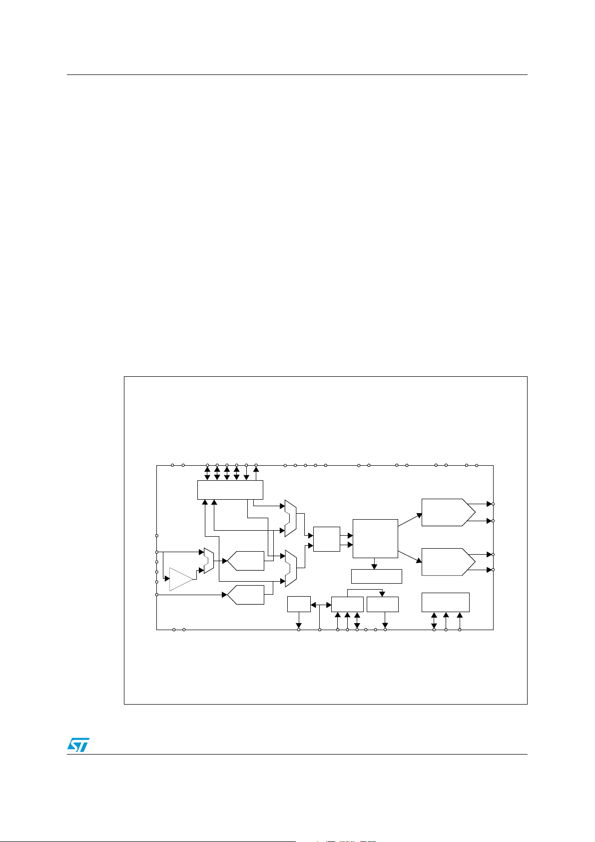
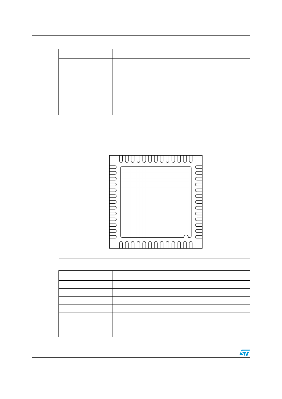
1 Description
The STA529 is a digital stereo class-D audio amplifier. It includes an audio DSP, an ST
proprietary high-efficiency class-D driver and CMOS power output stage. It is intended for
high-efficiency digital-to-power-audio conversion for portable applications. The STA529 also
provides output capabilities for FFX
provides high-quality digital amplification.
The STA529 contains an on-chip volume/gain control.
The PWM amplifier achieves greater than 90% efficiency for longer battery life for portable
systems.
The innovative class-D modulation, allows the STA529 to work without external LC filters
and without a heatsink.
The STA529 I2CDIS pin disables the audio DSP functions and the I
direct conversion of the input signal into output power. This conversion is done without the
microcontroller.
The STA529 is designed for low-power operation with extremely low-current consumption in
standby mode. It is available in packages TFBGA48 and VFQFPN52. These are very thin
packages (1.2 mm thick) ideal for small portable applications.
™
. In conjunction with a power device, the STA529
2
C interface provides a
Figure 1. Block diagram
BICLKO / PWM1A
LRCLKI
BICLKI
Serial digital
LRCLKO / PWM1B
ADC
ADC
VBIAS
INL
VHI
VCM
VLO
INR
VDD
PGA
AVC C
GND
audio interface
MUX
AGND
SDATAI
SDATAO / PWM2A
RST_NTMSTBY
MUX
MUX
XTO
MUTE
POWERFAULT / EADP
Digital
volume
XTI
MCLK33
SELCLK33
GNDIO
VDDIO
FFX
modulator
PWM out I/F
DividerPLLOSC
FILT
VDDPLL
GNDPLL
GND33
VCC33
GND2
GND1
Power
driver
Powe r
driver
Control
interface
SCL
SDA
VCC2
I2CDIS
VCC1
OUT1A
OUT1B
OUT2A
OUT2B
CLKOUT / PWM2B
Doc ID 13095 Rev 3 7/57
Connection diagrams and pin descriptions STA529
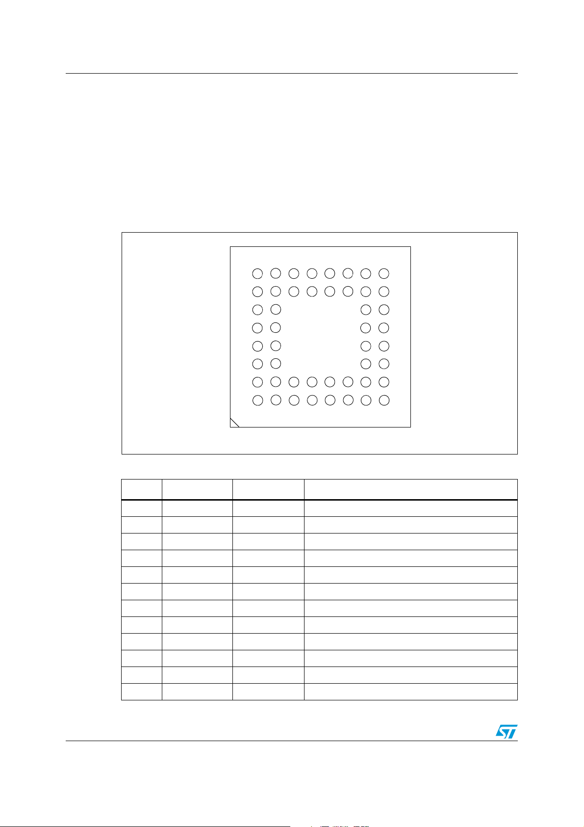
2 Connection diagrams and pin descriptions
This section includes connection diagrams and pin descriptions for the following packages:
● TFBGA48
● VFQFPN52
2.1 TFBGA48 package
Figure 2. Connection diagram for TFBGA48 (bottom view)
H
G
F
E
D
C
B
A
12345678
Table 2. Pin description for TFBGA48
Pin Name Type Description
A1 VCC2 Supply Channel 2 power supply
A2 GND2 Ground Channel 2 power ground
A3 OUT2A Analog output Channel 2 half-bridge A output
A4 OUT2B Analog output Channel 2 half-bridge B output
A5 OUT1B Analog output Channel 1 half-bridge B output
A6 OUT1A Analog output Channel 1 half-bridge A output
A7 GND1 Ground Channel 1 power ground
A8 VCC1 Supply Channel 1 power supply
B1 GNDIO Ground I/O ring ground
B2 GND33 Ground Pre-driver ground
B3 OUT2A Analog output Channel 2 half-bridge A output
B4 OUT2B Analog output Channel 2 half-bridge B output
8/57 Doc ID 13095 Rev 3
STA529 Connection diagrams and pin descriptions
Table 2. Pin description for TFBGA48 (continued)
Pin Name Type Description
B5 OUT1B Analog output Channel 1 half-bridge B output
B6 OUT1A Analog output Channel 1 half-bridge A output
B7 MUTE Digital input Mute (active high)
B8 GND Ground Digital ground
C1 VDDIO Supply I/O ring supply
C2 VCC33 Supply Pre-driver supply
C7
C8 VDD Supply Digital supply
D1 XTI
D2 XTO
D7 RST_N Digital input Reset (active low)
D8 VCM Analog I/O ADC common mode voltage
CLKOUT /
PWM2B
Digital output Buffered clock output / PWM2B FFX
Digital input
1.8V
Digital output
1.8V
Crystal input or master clock input
Crystal output
E1 MCLK33 Digital input Master clock input 3.3-V capable
E2 SDATAI Digital input Input serial audio interface data
E7 VLO Analog input ADC low reference voltage
E8 AGND Ground ADC analog ground
2
F1 SCL Digital input I
F2
POWERFAULT /
EAPD
Digital output
C serial clock
Power fault signal (active high) /
external audio power-down signal
F7 VHI Analog input ADC high reference voltage
F8 AVDD Supply ADC analog supply
2
G1 SDA Digital I/O I
G2 I2CDIS Digital input I
C serial data
2
C disable pin (active high)
Master clock input selector:
G3 SELCLK33 Digital input
0: XTI selected
1: MCLK33 selected
G4
G5
G6
SDATAO /
PWM2A
LRCLKO /
PWM1B
BICLKO /
PWM1A
Digital output Output serial audio interface data / PWM2A FFX
Digital I/O
Digital I/O
Output serial audio interface L/R-clock
(volume increases when I2CDIS = 1) / PWM1B FFX
Output serial audio interface bit-clock
(volume decreases when I2CDIS = 1) / PWM1A FFX
G7 VBIAS Analog I/O ADC microphone bias voltage
G8 STBY Digital input Standby (active high)
H1 FILT Analog I/O PLL loop filter terminal
Doc ID 13095 Rev 3 9/57
Connection diagrams and pin descriptions STA529
Table 2. Pin description for TFBGA48 (continued)
Pin Name Type Description
H2 TM Digital input Test mode (active high)
H3 GNDPLL Ground PLL analog ground
H4 VDDPLL Supply PLL analog supply
H5 LRCLKI Digital I/O Input serial audio interface L/R-clock
H6 BICLKI Digital I/O Input serial audio interface bit-clock
H7 INL Analog input ADC left channel line input or microphone input
H8 INR Analog I/O ADC right channel line input
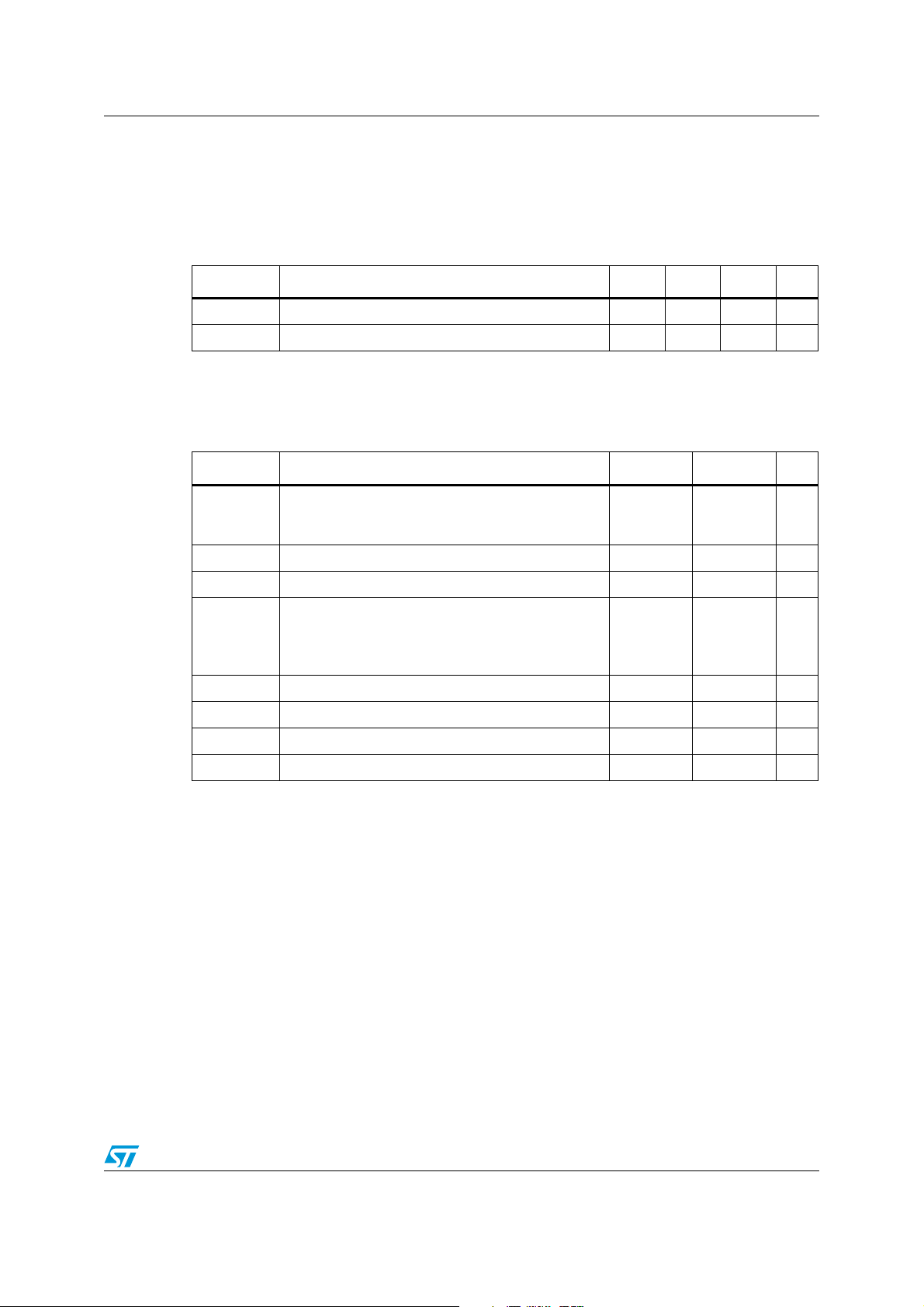
2.2 VFQFPN52 package
Figure 3. Connection diagram for VFQFPN52 (bottom view)
27
26
14
13
Table 3. Pin description for VFQFPN52
39
40
52
1
Pin Name Type Description
1 STBY Digital input Standby (active high)
2 INL Analog input ADC left channel line input or microphone input
3 INR Analog I/O ADC right channel line input
4 VBIAS Analog I/O ADC microphone bias voltage
5 AVDD Supply ADC analog supply
6 VHI Analog input ADC high reference voltage
7 VLO Analog input ADC low reference voltage
10/57 Doc ID 13095 Rev 3
STA529 Connection diagrams and pin descriptions
Table 3. Pin description for VFQFPN52 (continued)
Pin Name Type Description
8 AGND Ground ADC analog ground
9 VCM Analog I/O ADC Common mode voltage
10 RST_N Digital input Reset (active low)
11
12 GND1 Ground Digital ground
13 VDD1 Supply Digital supply
14 MUTE Digital input Mute (active high)
15 VCC1A Supply Channel 1 half-bridge A power supply
16 OUT1A Analog output Channel 1 half-bridge A output
17 GND1A Ground Channel 1 half-bridge A power ground
18 GND1B Ground Channel 1 half-bridge B power ground
19 OUT1B Analog output Channel 1 half-bridge B output
20 VCC1B Supply Channel 1 half-bridge B power supply
21 VCC2B Supply Channel 2 half-bridge B power supply
CLKOUT /
PWM2B
Digital output Buffered clock output / PWM2B FFX
22 OUT2B Analog output Channel 2 half-bridge B output
23 GND2B Ground Channel 2 half-bridge B power ground
24 GND2A Ground Channel 2 half-bridge A power ground
25 OUT2A Analog output Channel 2 half-bridge A output
26 VCC2A Supply Channel 2 half-bridge A power supply
27 GND33 Ground Pre-driver ground
28 GNDIO1 Ground I/O ring ground
29 VDDIO1 Supply I/O ring supply
30 VCC33 Supply Pre-driver supply
31
POWERFAULT /
EAPD
Digital output
Power fault signal (active high) / external audio power
down signal
32 TM Digital input Test mode (active high)
2
33 I2CDIS Digital input I
34 SCL Digital input I
35 SDA Digital I/O I
C disable pin (active high)
2
C serial clock
2
C serial data
Master clock input selector:
36 SELCLK33 Digital input
0: XTI selected
1: MCLK33 selected
37 MCLK33 Digital input Master clock input 3.3-V capable
38 XTI
Digital input
1.8V
Crystal input or master clock input
Doc ID 13095 Rev 3 11/57

Connection diagrams and pin descriptions STA529
Table 3. Pin description for VFQFPN52 (continued)
Pin Name Type Description
39 XTO
40 FILT Analog I/O PLL loop filter terminal
41 GNDPLL Ground PLL analog ground
42 VDDPLL Supply PLL analog supply
43 GND2 Ground Digital ground
44 VDD2 Supply Digital supply
45 SDATAI Digital input Input serial audio interface data
46
47 LRCLKI Digital I/O Input serial audio interface L/R-clock
48
49 GNDIO2 Ground I/O ring ground
50 VDDIO2 Supply I/O ring supply
51 BICLKI Digital I/O Input serial audio interface bit-clock
52
SDATAO /
PWM2A
LRCLKO /
PWM1B
BICLKO /
PWM1A
Digital output
1.8V
Digital output Output serial audio interface data / PWM2A FFX
Digital I/O
Digital I/O
Crystal output
Output serial audio interface L/R-clock
(volume increases when I2CDIS = 1) / PWM1B FFX
Output serial audio interface bit-clock
(volume decreases when I2CDIS = 1) / PWM1A FFX
12/57 Doc ID 13095 Rev 3
STA529 Electrical and thermal specifications
3 Electrical and thermal specifications
3.1 Thermal data
Table 4. Thermal data
Device Parameter Min Typ Max Unit
TFBGA48 Thermal resistance junction to ambient - 40 - °C/W
VFQFPN52 Thermal resistance junction to ambient - 22 - °C/W
3.2 Absolute maximum ratings
Table 5. Absolute maximum ratings
Pin/symbol Description Min Max Unit
VDD
VDD1
VDD2
AVDD ADC supply voltage -0.5 +4 V
VDDPLL PLL analog supply voltage -0.5 +2.5 V
Digital supply voltage -0.5 +2.5 V
VCC1A
VCC1B
VCC2A
Power stage supply voltage -0.5 +4 V
VCC2B
VCC33 Pre-driver supply -0.5 +4 V
VDDIO Digital I/O supply -0.5 +4 V
T
T
STG
J
Storage temperature -40 150
Junction temperature -40 150
Note: All grounds must be within 0.3 V of each other.
o
C
o
C
Doc ID 13095 Rev 3 13/57
Electrical and thermal specifications STA529
3.3 Recommended operating conditions
Table 6. Recommended operating conditions
Symbol Parameter Min Typ Max Unit
VDD
VDD1
VDD2
AVDD ADC supply voltage 1.8 3.3 3.6 V
VDDPLL PLL analog supply voltage 1.55 1.80 1.95 V
VCC1A
VCC1B
VCC2A
VCC2B
Digital supply voltage 1.55 1.80 1.95 V
Power stage supply voltage 1.8 3.0 3.3 V
VCC33
Pre-driver supply
(must be at same level as VCC1A/1B/2A/2B)
1.8 3.0 3.3 V
VDDIO Power supply for I/Os 1.8 3.0 3.6 V
GND1,
GND2,
Channel 1 and 2 power ground, pre-driver ground - 0 - V
GND33
GNDIO Ground for I/Os - 0 - V
IH 3.3-V supply 2.0 - - V
V
V
IL 3.3-V supply - - 0.8 V
HYST Schmitt trigger hysteresis (VDDIO) 0.4 - - V
V
T
AMB
Ambient operating temperature -40 - 85
o
C
14/57 Doc ID 13095 Rev 3
STA529 Electrical and thermal specifications
3.4 Electrical characteristics
The electrical specifications in Ta bl e 7 below are given for operation under the
recommended conditions listed in Ta bl e 6 . Unless otherwise specified, LRCLKI frequency
(fs) = 48 kHz, input frequency = 1 kHz, and R
Table 7. Electrical characteristics
Symbol Parameter Test conditions Min Typ Max Unit
Eff Output power efficiency - - 90 - %
R
dson
Output stage N/PMOS onresistance
= 32 Ω.
LOAD
- - 250 380 mΩ
IstbyL
IstbyP
IddL
IddP
Tds Low current dead time (static) - - 1 - ns
Tdd
Tr Rise time - - 3 - ns
Tf Fall time - - 3 - ns
DNR
SNR
THDN Total harmonic distortion
Logic power supply current at
standby
Bridges power supply current in
standby
Logic power supply current at
operating
Bridges power supply current at
operating
High current dead time
(dynamic)
Dynamic range
A-weighted
Signal-to-noise ratio (Aweighted)
--1.3-µA
--0.7-µA
--15-mA
--0.5-mA
--2.5-ns
Speaker mode - 96 - dB
Speaker mode - 92 - dB
0 dBFS input,
8 Ω speakers
-6 dBFS input,
8 Ω speakers
0 dBFS input,
32 Ω headphones
-0.1-%
-0.05-%
-0.1-%
-6 dBFS input,
32 Ω headphones
Doc ID 13095 Rev 3 15/57
-0.05-%
Electrical and thermal specifications STA529
The following tables give the output power for 1% and 10% THD levels for headphones and
speakers.
Table 8. Load power at 1% distortion in headphone mode
Load (Ω) P (mW) at 1.8 V P (mW) at 3.3 V
16 20 65
32 10 32
Table 9. Load power at 10% distortion in headphone mode
Load (Ω) P (mW) at 1.8 V P (mW) at 3.3 V
16 25 85
32 13 42
Table 10. Load power at 1% distortion in speaker mode
Load (Ω) P (mW) at 1.8 V P (mW) at 3.3 V
4 310 860
8 166 560
16 86 290
32 43 147
Table 11. Load power at 10% distortion in speaker mode
Load (Ω) P (mW) at 1.8 V P (mW) at 3.3 V
4 400 1100
8 216 720
16 112 380
32 57 200
3.5 Lock time
Ta bl e 1 2 gives the typical lock time of the PLL using the suggested loop filter with 1.8 V
supply and 30
Table 12. PLL lock time
Lock time 200 µs
o
C junction temperature.
Parameter Value
16/57 Doc ID 13095 Rev 3
STA529 Input clock
4 Input clock
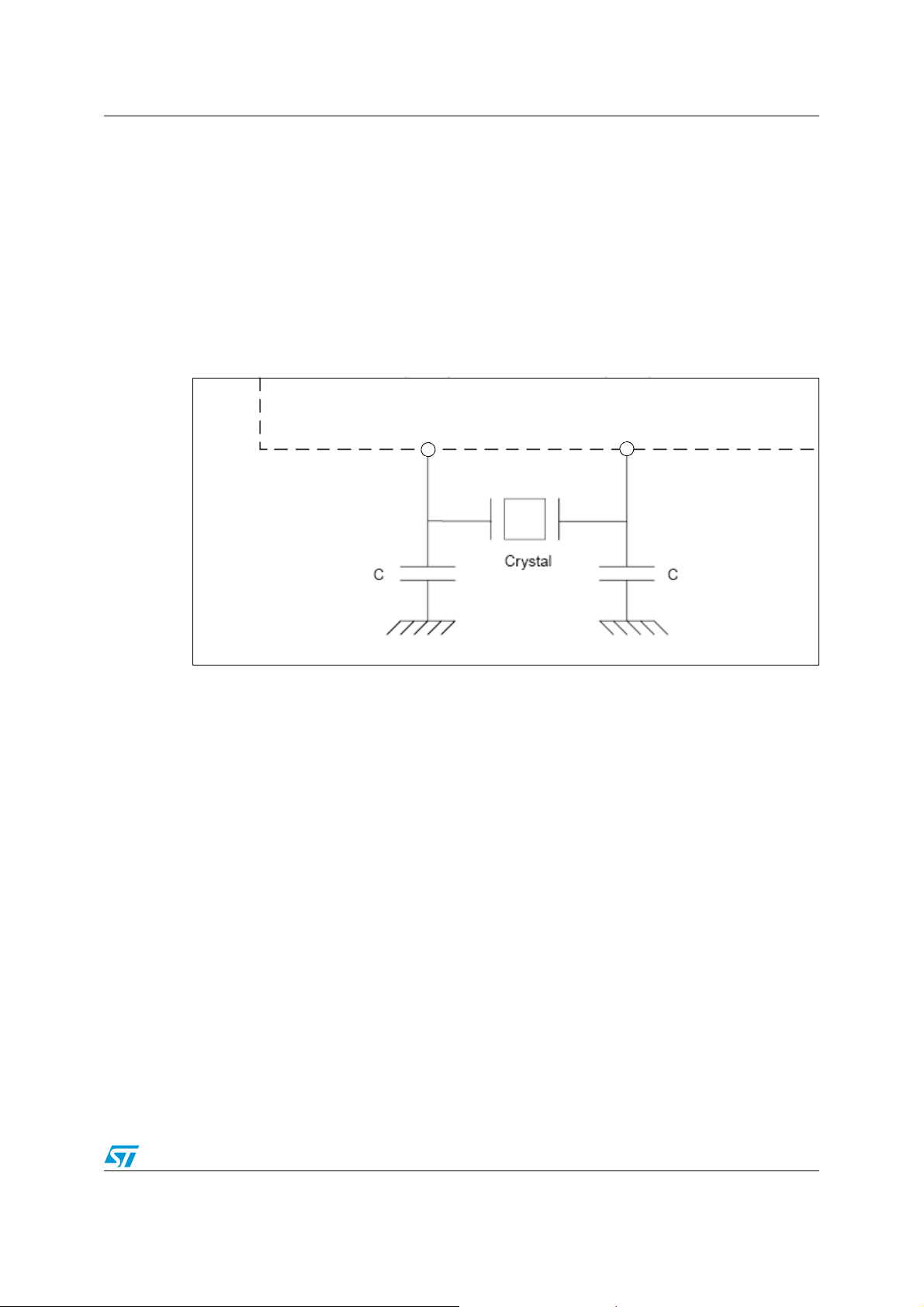
4.1 SELCLK33
In STA529 the oversampling clock comes from MCLK33 or from pin XTI. The selection is
done by applying the appropriate voltage to pin SELCLK33. If SELCLK33 is logical 1 then
MCLK33 is selected, otherwise XTI is selected.
If an external crystal is used, SELCLK33 pin must be connected to GND and the suggested
circuit shown below should be used.
Figure 4. Circuit for crystal drive
STA529
External
components
Doc ID 13095 Rev 3 17/57

Digital processing STA529
5 Digital processing
The STA529 processor block is a digital block providing two channels of audio processing
and channel-mapping capability.
5.1 Signal processing flow
I2S or stereo ADC data can be selected. The I2S frequency range is 8 kHz to 192 kHz. The
ADC sampling frequency can be selected between 8 kHz and 48 kHz.
5.2 I2C interface disable
When pin I2CDIS = 1, the SDA, SCL, LRCLKO and BICLKO pins can be pulled high or low
to change certain parameters of operation.
● SDA = 0: FFX input comes from ADC
SDA = 1: FFX input comes from digital audio interface
● SCL = 0: binary output mode (binary soft start/stop enabled)
SCL = 1: phase shift output mode
● LRCLKO = 0: no volume change
LRCLKO = 1: channel volume up on both channel
● BICLKO = 0: no volume change
BICLKO = 1: channel volume down on both xchannel.
At power up, the channel volume is set to -60 dB. When holding pin LRCLKO = 1 and pin
BICLKO = 1 simultaneously, the channel volume is set to 0 dB. A high pulse on pin LRCLKO
causes a channel volume change of +0.5 dB and a high pulse on pin BICLKO causes a
channel volume change of -0.5 dB.
18/57 Doc ID 13095 Rev 3
 Loading...